HAL Id: hal-03052755
https://hal.archives-ouvertes.fr/hal-03052755
Submitted on 10 Dec 2020
HAL is a multi-disciplinary open access
archive for the deposit and dissemination of
sci-entific research documents, whether they are
pub-lished or not. The documents may come from
teaching and research institutions in France or
abroad, or from public or private research centers.
L’archive ouverte pluridisciplinaire HAL, est
destinée au dépôt et à la diffusion de documents
scientifiques de niveau recherche, publiés ou non,
émanant des établissements d’enseignement et de
recherche français ou étrangers, des laboratoires
publics ou privés.
Millimeter-sized particle sensor using a wide field of
view monolithic lens assembly for light scattering
analysis in Fourier domain
Gabriel Jobert, Maryse Fournier, Salim Boutami, Cécile Jamois, Andrea
Lovera, Daniele Braga, C. Seassal
To cite this version:
Gabriel Jobert, Maryse Fournier, Salim Boutami, Cécile Jamois, Andrea Lovera, et al..
Millimeter-sized particle sensor using a wide field of view monolithic lens assembly for light scattering analysis
in Fourier domain. SPIE OPTO 2020, Feb 2020, San Francisco, United States. �10.1117/12.2544185�.
�hal-03052755�
Millimeter-sized particle sensor using a wide FoV monolithic lens
assembly for light scattering analysis in Fourier domain
Gabriel Jobert*
,a,b, Maryse Fournier
a, Salim Boutami
a, Cécile Jamois
b, Andrea Lovera
c, Daniele
Braga
c, Christian Seassal
ba
Université Grenoble-Alpes, CEA-LETI Minatec, F38000 Grenoble, France;
b
Institut des Nanotechnologies de Lyon, UMR CNRS 5270 Ecole Centrale de Lyon, Université de
Lyon, F-69134 Ecully, France;
c
FEMTOprint, Via Industria 3 Muzzano CH-6933
ABSTRACT
We present our latest advances in the field of miniature optical particulate matter sensors. By illuminating a single particle in an air channel, one can record the light scattering signature with a CMOS image sensor and then, classify particles. This signature is pre-processed optically with an advanced, millimeter-sized, monolithic, refracto-reflective optical system. It performs notably a Fourier transform with very wide FoV of scattering angles, and includes as well integrated fluidics and alignment. Functional prototypes were fabricated using laser micro machining on glass, selective polishing, and were replicated with epoxy resin using a molding process.
Keywords: Particulate matter; Light-scattering; CMOS image sensor; Miniature sensor; Miniature optics.
1. INTRODUCTION
Particulate Matter (PM) is a class of pollutant known to have serious medical impacts [1][2]. It is composed of suspended airborne particles of size ranging from a few nanometers to a few micrometers. In particular, the regulated subclass PM2.5
refers to particles smaller than 2.5µm. The IARC (International Agency for Research on Cancer) have classifiedPM2.5 as
a group 1 agent (known carcinogenic agent) [3]. In addition, a meta-analysis conducted by the US-EPA have concluded on the causality of premature death by PM2.5 exposure [4]. Beyond PM2.5, the unregulated subclass PM1 (particles smaller
than a micron) is highly suspected of being far more harmful than PM2.5 as it can penetrate the respiratory system deeper
[5].
1.1. Light-scattering & Miniature PM monitors
There is an urgent need for personal air quality monitors that are low cost and portable [6][7]. Indeed, the required spatio-temporal resolution of air quality (indoor and outdoor [8]) cannot be delivered by conventional air quality monitoring ground stationswe still rely on.
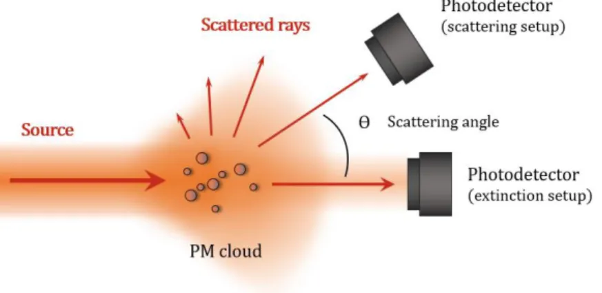
A vast field of techniques is capable of sensing particulate matter [9]. Although, we believe that the family of light scattering sensors is the most suited one for miniaturization. The light scattering set-up (already is used in the majority of existing low cost PM2.5 sensors) shows great simplicity and good sensitivity. The technique consists of a visible light
source (or near infrared) used for the illumination of an air chamber and a photo-detector deaxed with respect to the optical axis (see Figure 1). The latter, would only detect light that was deviated (i.e. scattered) by a particle the chamber.
Figure 1: Illustration of the light-scattering technique
Scaling down optical PM2.5 & PM1 sensors usually involves co-integration of light sources, photodetectors as well as
fluidics using techniques developed for silicon microfabrication, optronics and lab-on-chips [10][11]. In particular, our early designs includes planar photonic integrated circuits with active components such as a light source and photodiodes that are both coupled to passive optics such as silicon-based waveguides. The air channel is vertically drilled out of the substrate [12].
Particle concentration can be estimated from the total scattered intensity collected by the deaxed photodetector. However, useful information such as their nature and sizes remain unknown. Estimating these optical parameters (refractive index and diameter) is achievable by measuring the ‘light scattering signature’ of a particle.
1.2. Lorenz-Mie theory & scattering signatures
A particle’s ‘scattering signature’ is the scattering efficiency as a function of the angle. It depends on the geometry of the particle (shape and size), its refractive index and the wavelength of the excitation light in the surrounding medium. Being able to calculate such signature allow for the classification of particles [13].
The Lorenz-Mie theory [14][15] is the most common description of light-scattering. It solves the electromagnetic problem of a uniform sphere illuminated by a monochromatic plane wave. Despite its simplicity, this theory have proved itself quite robust.
This theory shows for example that the smaller the particle is (compared to the excitation wavelength), the more spherical the scattering signature is. For large particle (larger than a few wavelength), most of the scattered intensity is deviated with smaller angles and sides lobes appears as the diameter increases. The signatures varies also with the complex refractive index of the sphere.
2. DESIGNING THE OPTICAL SYSTEM
We have developed a first generation optical PM sensor that is the base frame for our new generation PM sensor (see hereafter). The former is able to count and record a particle’s scattering signature projected onto a holed CMOS image sensor (that a both a detector and a fluidic channel). More details are presented on the very same conference [16] (unpublished reference). Similar designs are also found in conference papers [17][18] and in patent [19].
The signature recorded is optically transformed through a planar, lens-free projection with a short working distance. The geometry was optimized to maximize both the sensitivity of low intensity scattered light as well as the Field of View (FoV) of scattered angles. We abusively define the Field of View (FoV) by the range of evaluated scattering angles. In the first generation PM sensor, the FoV is limited by the geometry as we can evaluate scattering signatures within a FoV of only a few tens of degrees. There is little margin of improvement that can be made using the lens-free planar projection. Moreover, the uncertain position of the particle within the illumination beam can result in an affine transformation of the image as well as a blurring effect, with a shifted range of evaluated scattering angles. This last part is taken into account by our image analysis procedure but one may want to simplify the computing part as much as possible for future portable applications.
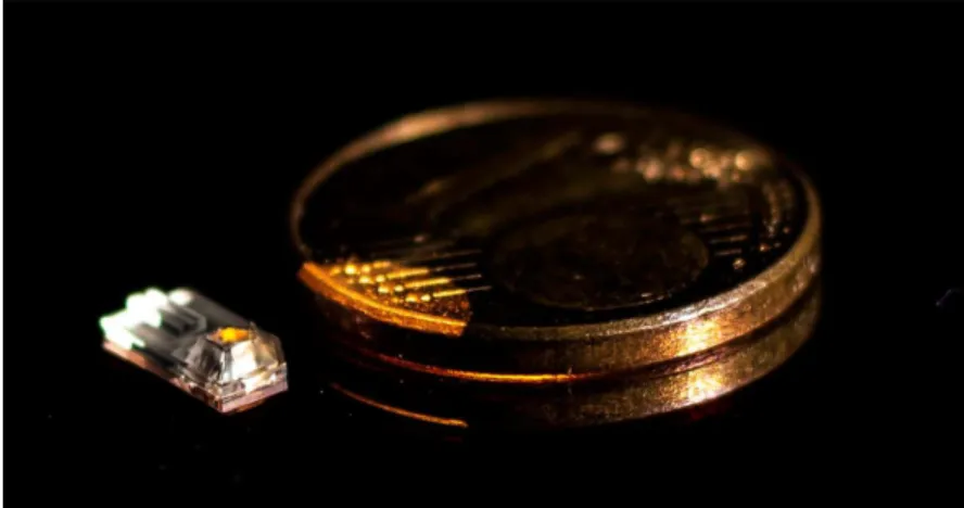
This document aims to present a way to answer some of the identified problems with the direct projection: the narrow field of view and the influence of the position of the scattering particle. The suggested solutions, and other additional improvements, resulted in the design and fabrication of our miniature optical system shown in Figure 2. This piece was made from a single fused silica glass substrate and contains several optical surfaces, alignments and fluidics. It is contained within a small volume of about 3 mm x 6 mm x 1 mm. More information can be found in patent [20].
Figure 2: Photography of the miniature lens system next to one cent coin (EU)
2.1. Position insensitivity
In most, non-miniaturized, light-scattering photometers, the position of the particle does not interfere much with the measurements. Indeed, the range of positions allowed for the particle is very small compared to the optical path of scattered rays. Noteworthy, errors induced by particle position have been reported by others teams that are also working on scaling down their sensors [21].
In our case, the errors induced by particle position includes translation, magnification and rotation of the recorded image; a superposition of shifted signatures can be generated by clouds of particles, resulting in a position blur; as a corollary, the detection of a moving particle (with respect of the integration time of the image) results in a motion blur.
In short, position insensitivity can be achieved in a far-field set-up. An equivalent set-up is the common d-f lens system: The detector array is placed at the image focal plane of a thin lens (simplified model) so that the object is seen at infinity. Consequently, the detector can record an angular image by refocusing parallel rays.
If the object is a particle (or a cloud of particles), considered a punctual source, at an unspecified position and casting rays whose intensity varies according to the scattering angle. The detector array will then record directly the scattering signature. The image taken isn’t modified by displacing the particle as the same scattered rays are always seen under the same angles, see Figure 3.
Using Fourier’s harmonic description of the d-f set-up [22], one can show that the information on the position of the particle is only carried by the phase of the wave at the image focal plane of the lens. The angular image (i.e. the scattering signature) is carried by the amplitude of the wave at this focal plane. A simple photo-detector array like ours is only sensitive to the amplitude: the recorded image in purely an image of the scattering signature, in the Fourier domain. This optical pre-treatment of the scattering signature dramatically simplifies the analysis of the image taken by the retina, removing the need of energy costly image processing algorithms.
2.2. Asymmetric crown shape
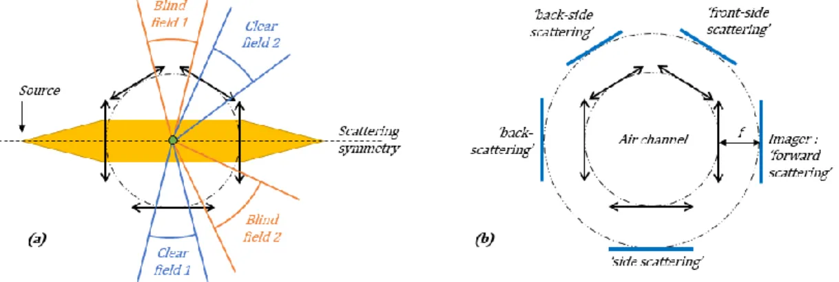
Let us consider a lens system coupled to a detector array. A factor that limits of field of view (FoV) is, for instance, the pupil of the system. The idea behind improving the FoV for light scattering analysis is merging several of these subsystems around a perpendicular air channel in a crown shape.
The edges of each subsystem may contain aberrations or unwanted artefacts we call ‘blind fields’ especially at the limit of two merged ones were we may observe cross-talk effects between the subsystems.
By taking advantage of the symmetry of the scattering signature around the optical axis, one can sacrifice a bit of redundancy by facing half of the lenses toward the blind fields of the other halves. Resulting design is the asymmetric crown shape with an uneven number of optical subsystems arranged around a perpendicular air channel. An example is shown in Figure 4 with five subsystems (modeled as thin lenses).
Figure 4: Principle of blind fields asymmetrically coupled to clear fields (a). Lenses coupled with imagers in Fourier planes
In this design, the FoV can be – in theory - as wide as 180°. The limiting factor is the surface bloomed by the illumination beam (which is orders of magnitude compared to the scattered intensity). For a collimated beam (as in Figure 4), the bloomed area is at best, the size of the diffraction spot of our optics plus the point spread function of our retina. For a diverging (or converging) beam, the bloomed area is convoluted with associated angles within the beam divergence.
2.3. Compact optical subsystems with coincidental Fourier planes
Each optical subsystem must meet a certain set of specifications: it must be as compact as possible, it must also fold its Fourier plane (i.e. image focal plane) onto a plane perpendicular to the fluidic channel so that all subsystems Fourier planes are coincidental. This set-up enables to use a single holed retina (in a similar fashion than our first generation PM sensor) to image all Fourier planes on separate regions of interest.
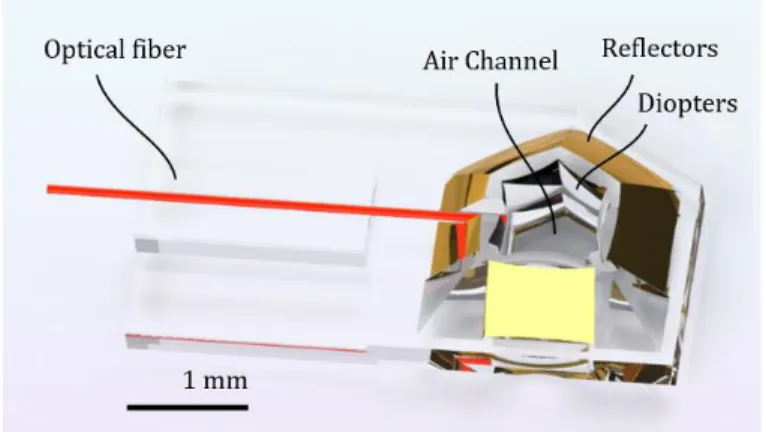
We design in Figure 5 an optical subsystem composed of two spherical diopters and a 45° spherical internal reflector that folds the image focal plane. The surface can be covered with a metallic reflective layer such as aluminum or gold. Alternatively, no reflective layer is used as the internal reflections within the material can be efficient enough.
Figure 5:3D design of the refracto-reflective optical subsystem
Every surface participates in the function of focusing the rays so that we can obtain a good optical system with few aberrations for our application and a short back focal length (BFL = 0.37 mm).
The subsystem takes advantage of three surfaces out of a same volume, thus can be manufactured out of a unitary piece. For this prototype, the material used for the design is a fused silica glass, but it can also work with most optical polymers. This refracto-reflective subsystem (Figure 5) was designed using the optimization tools from Zemax Optic Studio software in sequential mode.
Compactness is then improved by truncating such optical surfaces. 2.4. Subsystem merging and fiber alignment
Five identical optical subsystems are merged into a unitary piece. The resulting model is rendered in Figure 6. It contains the merged subsystems around a vertical fluidic channel. Note that the front surfaces (first diopters) are part of the inside walls of the channel.
Figure 6: Rendering of the miniature optical system
We also design a V-groove that continues through the back subsystem and stops at the edge of the channel. This V-groove allows an easy alignment of a standard pigtailed optical fiber (125 µm of diameter). The fiber can illuminate the channel forming a beam with a divergence defined by the numerical aperture (NA) of the fiber.
This piece is designed to be manufactured from a single, 1 mm thick, fused silica substrate. 2.5. Angular response at the coincidental Fourier plan
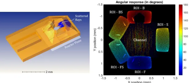
We present a simulation (ray tracing) of the silica glass piece in Figure 7. For the reader comprehension, we have simplified the scattering particle down to a simple conical source point. Left figure shows the propagation of rays casted by five randomly positioned particles. We verify that the resulting image on the Fourier plane isn’t impacted by particle’s position.
Figure 7: Ray Tracing simulation of the optical system (left). Angular (color) map in the focal plane (right)
The right figure presents the angular response of the optical system. We verify that a point in the focal plane is associated to a scattering angle. We also recognize the five regions of interest (ROI) associated with the five optical subsystems. These ROIs allow us to evaluate the scattering signature thanks to the associated overlapping FoVs.
Note that we observe luminous “claw marks” at blind fields at the edge of two adjacent subsystems. These defects are cross talk effects between the systems meaning that rays can enter through a first diopter and exit through a last diopter’s adjacent system.
3. FABRICATION PROCESS
3.1. Micromachining on glass
The optical system was manufactured by the company FEMTOprint with an innovative 3D fabrication method for glass [23][24]. The fabrication protocol is composed by three main steps: laser exposure, wet etching and polishing.
The laser exposure was performed on a f200a Head enhanced machine starting from a 1 mm thick fused silica glass wafer. The substrate was exposed with a focused femtosecond laser beam at 1030 nm, properly shaped and focused with a 20x objective (Thorlabs, NA=0.4). The exposure conditions trigger a non-linear absorption process that causes a densification within the laser voxel. As consequence, the etching rate of the material for a KOH solution increase up to 1000 times compared to the un-exposed material [25]. By moving the sample and the beam we created the image of the object within the substrate.
Later, the wafer was immersed in a water solution of KOH (45%) at 80°C for 10h. During the etching the part is realized from the wafer. At the end, the device is cleaned with water and dried before the quality control. Since the etching process has a finite selectivity and is quite long, the original design was pre-compensated in order to achieve the desired dimensions after 10h.
The machined surfaces showed a roughness around 80 nm (Ra) on the vertical sidewalls (channel-facing front diopters) and 150-300 nm (Ra) on the planar or 3D surfaces (reflecting surfaces and back diopters). For this reason, a proprietary polishing process polishing was introduced to reduce the roughness of the optical elements below 30 nm by reflowing the surface with limited deformation.
Figure 8: Optical image of the fabricated optical system
3.2. Molding and replication
In this section, we explore the process of replicating our printed optical systems to achieve cost effectiveness. We show preliminary tests with a discarded glass prototype (polishing-induced deformation test sample) we will call ‘mother’ in this section.
We use PDMS (silicone) for the molding material. For complex 3D pieces like this one, the mold is made of two part: the bottom part is molded and dried first so that the upper part can be molded in turn. A picture of the glass prototype inside its mold is shown in Figure 9 (left).
Figure 9:Photography of the mother molded in PDMS (left). Cross sectional view of the unmolding step (right)
Despite the delicate surfaces of the channel inner walls, the unmolding step went smoothly. We observe no degradation of the mother after being molded and unmolded. The low roughness of the original glass piece appears to be well transferred into the mold.
This PDMS mold is then used to shape a replica (call ‘daughter’ hereafter) with an optical polymer. Here, we use a commercial transparent clear epoxy resin.
Figure 10: Glass prototype ('mother') next to its epoxy resin replica ('daughter') (a). Optical image of the daughter with a fiber installed (b)
A photography of the resulted replica is shown in Figure 10(a) next to the original glass prototype. Apart from the different refractive index of the materials, the surface quality of the lenses appears identical. The shapes are also recreated with great fidelity even inside the channel and with the V-groove that can hold an optical fiber with great precision (as shown in Figure 10(b).
4. CHARACTERIZATIONS
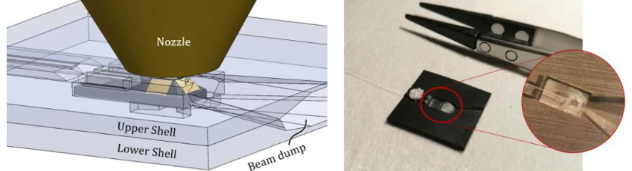
Preliminary tests were performed with the optical system separately (without a holed retina). To do so, we packaged our optical system with an upper and a lower shell (see Figure 11) that were fabricated with a black resin using a high resolution (25 µm voxel) 3D printer (Form 2 printer by Formlabs).
Figure 11: (left) Assembled 3D models of the shells. (right) Photography of the lower shell hold the lenses aligned with a fiber.
The shells contains a housing with precise dimensions for the optical system, an upper 1 mm circular air channel aligned with a metallic nozzle, an opening in front of the back diopters, an additional V-groove and beam-dump for stray light evacuation.
The air stream is injected into the upper part through the nozzle so that the optical path isn’t obstructed by fluidic parts. In a future set-up, the air-stream will be injected trough a lower holed retina as it prevents particle soiling.
We use a multimode pigtailed fiber (MMF 105/125) with low divergence (NA = 0.1) illuminated by an AlGaInP laser diode operating at a wavelength of 637 nm and with an optical power of 5 mW (HL63102MG by Oclaro).
The focal plane isn’t accessible in this set-up but we can project it using a microscope objective (NPL 10x/0.2 NA objective by Leitz Wetzlar) in reverse orientation and focused on a bared Global Shutter CMOS monochromatic image sensor (Thorlabs USB2.0 CMOS Global Shutter camera).
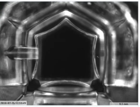
Figure 12:Reference image taken with light on and no air stream
We take a reference image with light on and no air stream shown in Figure 12. The sensing area was previously cleaned up with dry air. Every image of scattering signatures will be subtracted with this reference.
We observe that the forward region of interest (F-ROI) is completely bloomed by the illumination beam, the backward ROI (B-ROI) is partially bloomed by the scattering at the end of the fiber. These yellow surfaces are blind areas beyond the dynamics of the pixels.
However, the BS, S and FS ROIs receive very few stray light. Therefore, we will evaluate only these three ROIs to reconstruct scattering signatures with total FoV as wide as 90°.
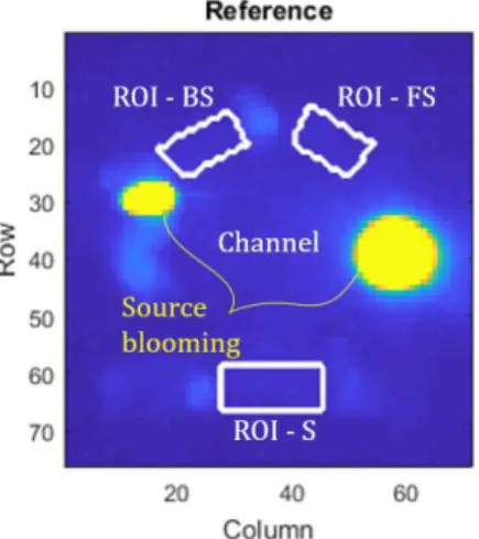
An example of a measured scattering signature is shown in Figure 13. It was obtained by spaying particles from an aerosol canister (Smoke Check HIS Canned Smoke by InspectUSA) in the nozzle.
Figure 13: Example of experimental image (left) and reconstructed signature (right)
The left figure is the image obtained (reference subtracted) in the presence of the aerosol. We evaluate pixels within the FS, S and BS ROIs (white contours) and we associate every pixels to an angle following our angle map calculated by ray-tracing (see Figure 7, right). This allows us to draw three curves and reconstruct a scattering signature (right figure). Through several tests, the signature is obtained with very good repeatability.
The reconstruction of the signature was extremely simple compared to the planar projection set-up. The procedure should be compatible with low energy portable applications.
Note that the curves aren’t perfectly overlapping: the edges of the individual curves correspond to blind field and must not be trusted too much. This overlapping mismatch will not bother us much as it appears to be very constant and is very certainly linked to how the different optical subsystems were truncated (i.e. their pupils).
5. CONCLUSION & PERSPECTIVES
In conclusion, we have designed a miniature, monolithic refracto-reflective system suited for the optical pre-treatment of the scattered signature. This design is applied to our family of particulate matter sensors with holed retina. It responds to the various areas of improvements identified such as particle’s position insensitivity, ultra wide field of view, alignment and simplified image processing.
We propose a fabrication process for a glass prototype that was developed by the FEMTOprint company as well as a replication process. Preliminary tests have shown good results reconstructing scattering signatures within a FoV of 90 degrees.
Planned tests includes a full set-up with the optical system mounted on an existing holed retina. Other tests consist in measuring scattering signatures and limits of detection (LoD) of single calibrated laboratory particles in our aerosol test bench.
Finally, we develop designs that are even more advanced. It included free-form internal reflectors designed to improve on the point spread function (PSF) of a folded optical subsystem. It also features new integrated functions within the glass substrate conceived in the mind of reducing stray light and cross talk effects: improving on the sensitivity.
ACKNOWLEDGEMENTS
The authors are thankful for the help from the FEMTOprint team for the fabrication of the glass optical system, in particular for Giulia Bottarini who has been a privileged interlocutor on this collaboration. We also recognize the invaluable help of Pierre Barritault and Mathieu Dupoy for their expertise on the experimental side as well as Véronique Mourier and Dominique Lauro for their contribution to the molding and replication process. Finally, we acknowledge Sergio Nicoletti, Laurent Duraffourg for supporting the project.
This project is funded by the Department of Optics and Photonics of the CEA-Leti (France). The project is part of the doctoral activities of the primary author and followed academically by the University of Lyon (France).
REFERENCES
[1] G. B. Hamra et al., « Outdoor Particulate Matter Exposure and Lung Cancer: A Systematic Review and Meta-Analysis », Environ. Health Perspect., juin 2014.
[2] J. O. Anderson, J. G. Thundiyil, et A. Stolbach, « Clearing the Air: A Review of the Effects of Particulate Matter Air Pollution on Human Health », J. Med. Toxicol., vol. 8, no 2, p. 166‑175, juin 2012.
[3] A. J. Cohen, J. M. Samet, K. Straif, et International Agency for Research on Cancer, Air pollution and cancer. Lyon: International Agency for Research on Cancer, 2013.
[4] « Integrated Science Assessment for Particulate Matter (External Review Draft, 2018) », U.S. Environmental Protection Agency, Washington, DC, 2018.
[5] S. A. Cormier, S. Lomnicki, W. Backes, et B. Dellinger, « Origin and Health Impacts of Emissions of Toxic By-Products and Fine Particles from Combustion and Thermal Treatment of Hazardous Wastes and Materials »,
Environ. Health Perspect., vol. 114, no 6, p. 810‑817, juin 2006.
[6] E. G. Snyder et al., « The Changing Paradigm of Air Pollution Monitoring », Environ. Sci. Technol., vol. 47, no 20,
p. 11369‑11377, oct. 2013.
[7] Francesca Borghi et al., « Miniaturized Monitors for Assessment of Exposure to Air Pollutants: A Review », Int. J.
Environ. Res. Public. Health, vol. 14, no 8, p. 909, août 2017.
[8] B. C. Singer et W. W. Delp, « Response of consumer and research grade indoor air quality monitors to residential sources of fine particles », Indoor Air, vol. 28, no 4, p. 624‑639, juill. 2018.
[9] S. Amaral, J. de Carvalho, M. Costa, et C. Pinheiro, « An Overview of Particulate Matter Measurement Instruments », Atmosphere, vol. 6, no 9, p. 1327‑1345, sept. 2015.
[10] X. Li et al., « Miniaturized particulate matter sensor for portable air quality monitoring devices », in IEEE
SENSORS 2014 Proceedings, Valencia, Spain, 2014, p. 2151‑2154.
[11] M. Dong, E. Iervolino, F. Santagata, G. Zhang, et G. Zhang, « Silicon microfabrication based particulate matter sensor », Sens. Actuators Phys., vol. 247, p. 115‑124, août 2016.
[13] D. Weinert, T. Cleary, G. Mulholland, et P. Beever, « Light Scattering Characteristics And Size Distribution Of Smoke And Nuisance Aerosols », Fire Saf. Sci., vol. 7, p. 209‑220, 2003.
[14] C. F. Bohren et D. R. Huffman, Absorption and scattering of light by small particles. Wiley, 1983. [15] H. C. van de Hulst, Light Scattering by Small Particles. Dover Publications, 1981.
[16] M. Fournier et al., « A miniaturized optical sensor for particulate matter counting and classification », présenté à Photonics West, San Francisco, 2020.
[17] G. Jobert et al., « A Miniaturized Optical Sensor for Fire Smoke Detection », in 2019 20th International Conference
on Solid-State Sensors, Actuators and Microsystems & Eurosensors XXXIII (TRANSDUCERS & EUROSENSORS XXXIII), Berlin, Germany, 2019, p. 1144‑1149.
[18] S. Boutami et al., « Visible to mid-infrared integrated sensors for air quality measurement », in Optical Sensing,
Imaging, and Photon Counting: From X-Rays to THz 2019, San Diego, United States, 2019, p. 25.
[19] S. Boutami et S. Nicoletti, « Optical detector of particles », 2018W0-EP51890, 25-janv-2017. [20] G. Jobert, « Détecteur optique de particules », B03897 FR-DD18825 HB, 16-juill-2018.
[21] J. Pribošek et G. Röhrer, « Estimation of the Particle Sizing Error Due to Particle Position in an Integrated PM2.5 Optical Particle Counter », Proceedings, vol. 2, no 13, p. 850, déc. 2018.
[22] B. E. A. Saleh et M. C. Teich, Fundamentals of Photonics. New York, USA: John Wiley & Sons, Inc., 1991. [23] Y. Bellouard, « The Femtoprint Project », J. Laser MicroNanoengineering, vol. 7, no 1, p. 1‑10, févr. 2012.
[24] D. M. Krol, « Femtosecond laser modification of glass », J. Non-Cryst. Solids, vol. 354, no 2‑9, p. 416‑424, janv.
2008.
[25] C. A. Ross, D. G. MacLachlan, D. Choudhury, et R. R. Thomson, « Optimisation of ultrafast laser assisted etching in fused silica », Opt. Express, vol. 26, no 19, p. 24343, sept. 2018.