Chemical Vapor Etching of GaAs by CH31
byCharles Winslow Krueger BS, Chemical Engineering University of Pennsylvania, 1986 MS, Chemical Engineering Practice Massachusetts Institute of Technology, 1987
Submitted to the Department of Chemical
Engineering in Partial Fulfillment of the Requirements for the Degree of
Doctor of Philosophy in Chemical Engineering at the
Massachusetts Institute of Technology February, 1994
0 1994 Massachusetts Institute of Technology All rights reserved
Signature of Author
Certified by
Certified by
Departme/t of Chemical Engineering February 15, 1994
Dr. Maria /Flytzadi-Ste nopoulos Thesis Supervisor
Professor Robert A. Brown Thesis Supervisor Accepted by
Professor Robert A. Cohen UT;'-hairman, Committee for Graduate Students
HFEB
18 1994Chemical Vapor Etching of GaAs by CH3I by
Charles Winslow Krueger
Submitted to the Department of Chemical
Engineering on December 13, 1993 in Partial Fulfillment of the Requirements for the Degree of
Doctor of Philosophy in Chemical Engineering
Abstract
The etching reaction of CH3I vapor with gallium arsenide (GaAs) single crystals has been experimentally investigated in a cold wall, horizontal, atmospheric pressure gas flow reactor. This etching process was studied for application as a complementary in situ etch in organometallic vapor phase epitaxy (OMVPE) reactors. The
requirements for applying this etch process are that the surfaces be etched smoothly and free of any chemical contamination. A series of parametric experiments was performed in order to determine the optimum etch conditions.
Etching was also studied on substrates patterned with inert masks and on substrates with different crystallographic orientations. The effects of adding an arsenic source, trimethylarsenic, to the etch mixture was also investigated. Finally an etch mechanism was postulated based on the results of etch rate studies and the identification of etch products. This mechanism was tested by comparing simulated etch rates to experimentally observed etch
rates. The etch is seen to occur under a condition of gas phase kinetic control with the decomposition of CH3I in the gas phase being the
rate limiting step.
Thesis Supervisor: Maria Flytzani-Stephanopoulos Title: Principal Research Associate
Thesis Supervisor: Robert A. Brown Title: Professor
Acknowledgements
I would like to thank my advisors Miretta Stephanopoulos and Bob Brown for their guidnance and support over the years of this project. Chris Wang, who tolerated my presence in her lab for so many years, deserves something beyond normal gratitude. My other two
committee members, Karen Gleason and Leslie Kolodzieski have also been most helpful over the years.
The folks at Lincoln Laboratory and Group 83 - so many of whom contributed in small and large ways - receive a collective thankyou. I would like to further acknowledge the help I received in the early
going from Dave Tracy and Don Kolesar who taught me many things about working with my hands and about life in general. Dave Hovey and Jon McMillan from the glass shop were invaluable over the years. Mary Finn, for her reliable Auger analysis and Paul Nitishin for his SEM work deserve special recognition. Additionally special thanks go to Gerry Iseler, George Turner, and Hong Choi who allowed me into their labs at various times without always knowing exactly what I was doing. Mike Connors for doing the nitride depositions and Bill McGilvary for his help in the photolithography lab and for many enjoyable conversations. Additionally I want to thank Dorothy Hsieh for an enjoyable and productive summer during her tenure as a UROP student.
I want to thank Beth for her friendship, companionship and support over the years. My roommates, John, Dave, Bob, and Chris for keeping life outside of school entertaining. And all the rest of my friends from MIT. And last, but not least, my parents and family.
Contents
1 Introduction 1.1 Motivation 1.2 Objectives
1.3 Method of Approach
2 Background: Chemical Vapor Etching Techniques 2.1 Thermochemical Vapor Etching of GaAs
2.1.1 Chlorine (C12) Vapor Etching of GaAs
2.1.2 Hydrogen Chloride (HCl) Vapor Etching of GaAs 2.1.3 AsC13 Vapor Etching of GaAs
2.1.4 Bromine Vapor Etching of GaAs
3 Chemical Vapor Etching of (100) GaAs and AlxGal.xAs by CH3I and OMVPE Regrowth of GaAs
3.1 Introduction 3.1.1 Background 3.1.2 Objective 3.2 Experimental Procedure 12 14 14 15 20 23 24 26 26 27 29 30
3.2.1 Horizontal Reactor System 3.2.2 Substrate Preparation
3.2.3 Experimental Procedure: Etch Rate Studies 3.2.4 Experimental Procedure: Regrowth Studies 3.2.5 Analysis of Reactor Operation
3.3 Experimental Results and Discussion
3.3.1 Vapor Etching in the Horizontal Reactor: Etch Rate Parametric Studies
3.3.2 Etching in the Horizontal Reactor: Surface Morphology
3.3.3 Etching in the Horizontal Reactor: Carbon Deposition on Etched Surfaces
3.3.4 OMVPE Growth of GaAs on CH3I Vapor Etched
Substrates 3.4 Conclusion
Etching of Patterned GaAs Substrates by CH3I
4.1 Introduction 4.1.1 Objective 4.1.2 Background 4.2 Experimental Procedure 30 31 33 37 38 42 42 51 61 66 75 76 76 77 78 81 4 Vapor
4.2.1 Lateral Diffusion Studies
4.2.2 (111)A and (111)B GaAs Etch Rate Studies 4.2.3 Microfacet Etch Studies
4.3 Experimental Results and Discussion
4.3.1 Inert Mask Effects on Vapor Etching
4.3.2 Vapor Etching of Bulk Substrates of (111)GaAs by CH3I
4.3.3 CH3I Vapor Etching of Faceted Structures of
GaAs; Interactions Between Surface
81 83 83 86 86 102
Heterogeneities and Lateral Diffusion Processes 109 4.3.4 Mask Alignment Strategies, Orientation Effects
and Etch Anisotropies 113
4.4 Conclusions 117
5 The Mechanism of CH3I Vapor Etching of GaAs 5.1 Introduction
5.2 Gas Phase Chemical Reaction Set
5.3 Mass Spectrometer Study of CH3I Decomposition 5.4 Etch Product Analysis
118 118 120 122
131 5.5 CH3I Vapor Etching in the Vertical Rotating Disk Reactor:
5.4.1 Introduction
5.4.2 Details of Numerical Model
5.4.3 Verification of Computed Temperatures: Comparison of Measured Reactor Wall Temperatures with Model Predictions 5.4.4 Vapor Etching Rates: Comparison of Model
with Experiment and Other Predictions 5.5 Conclusions
16 Vapor Etching of GaAs with CH3I: Surface Reactions 6.1 Introduction
6.2 Background
6.3 Experimental Procedure
6.4 Experimental Results and Discussion 6.4.1 Results
6.4.2 Discussion 6.5 Conclusions
7 Summary and Recomendations 8 Bibliography
A. Vapor Etching with HI and (CH3)2N2
136 138 141 144 153 155 155 156 158 160 160 164 170 171 174 180
Chapter 1
Introduction
1.1 MOTIVATION
Epitaxial growth of crystalline semiconducting materials is an
important process for fabricating thin layers of high quality material. Chemical vapor deposition (CVD) epitaxial growth processes are an important technology which includes organometallic vapor phase epitaxy (OMVPE), a growing technology which involves the use of one or more organometallic precursor species. The continued importance of these technologies provides a major motivation for the subject of this thesis, the chemical vapor etching of gallium arsenide (GaAs). Chemical vapor etching is the reverse analog to CVD and is easily implemented into existing CVD/OMVPE reactor systems in situ, allowing for increased process flexibility by combining growth and etching into one reactor system.
For a vapor etching process to be applied to semiconductor
processing, the etched crystal surface should be mirror smooth. This is typically accomplished if material is etched in a layer by layer fashion. In addition, the etch process should introduce no chemical impurities or residues on the surface. Temperature is an important process parameter due to undesirable effects of dopant and/or alloy interdiffusion (Kuech, et al, 1988). These solid state diffusion
processes are generally highly activated motivating the need to develop a vapor etching process at low temperatures. Other issues include the ability to etch at uniform rates over wide areas and to controllably reproduce etch rates.
The etchant source compound that has been chosen for this study is methyliodide (CH3I). This chemical has been chosen for several
reasons. It is known to decompose into methyl radicals and iodine atoms at temperatures above 4000C (Saito, et al, 1980), both of these
free radical species are expected to be potential etchants. The
compound is a liquid at room temperature (bp = 430C) making it easy to handle and easy to implement into existing CVD/OMVPE reactor systems with a conventional bubbler/carrier gas arrangement. It is non-flammable but has toxic properties and should be handled accordingly. The undecomposed compound is non-corrosive so
upstream contamination problems are avoided, although some iodine compounds produced from its decomposition (I2, HI) are expected to be corrosive to downstream components of a reactor system.
The semiconductor material which is the main object of this study is gallium arsenide (GaAs). GaAs is a III-V crystalline compound and is probably the most technologically important semiconductor material after silicon. For example, a subject search on the Applied Science Index for 1992 revealed over 900 references to silicon, over 500 references to GaAs with other materials such as indium phosphide, indium arsenide and aluminum gallium arsenide each having on the order of 100 or fewer references. It is thereby seen that gallium
arsenide is an important semiconductor material. GaAs exhibits several desirable material and electrical properties. The theoretical electron mobility is nearly 30 times higher than for silicon, meaning
that circuits fabricated using GaAs in place of silicon should be 30 times faster. GaAs, unlike silicon, has a direct band gap, a property
that allows the material to be used as a light waveguide and permits fabrication of semiconductor lasers based on this property. These
devices would be employed in the future development of an optical computer. At this time the major limitations to using GaAs in place of
silicon have to do with processing the material into micron and submicron scale devices.
Studying vapor etching can also provide fundamental information into the general class of gas-solid reactions such as CVD and OMVPE. Reactions of free radicals with the semiconductor material can occur as side reactions in the industrially important processes of reactive ion etching (RIE) and other plasma-activated, isotropic etch
processes, which can lead to polymer deposition and undercutting of masked features which are generally undesirable. (Sidewall polymer deposition is often desired for suppressing sidewall etching reactions. Nevertheless, this deposition inevitably leaves chemical impurities
on the sidewalls). Recently, RIE of GaAs with iodine and methane containing gasses has been succesfully demonstrated (Pearton, et al,
1.2 OBJECTIVES
There are two main objectives of this thesis which are concerned with applying the CH3I vapor etch in situ of OMVPE reactor systems.
The first objective was to demonstrate the chemical vapor etching of GaAs by CH3I and determine operating conditions under which
etched surfaces are free of morphological imperfections and chemical impurities. These characteristics are necessary if the etch is to be employed as an in situ substrate cleaning process. A test of the etch process is to determine the quality of OMVPE GaAs deposited on etched surfaces.
The second objective is to examine CH3I vapor etching on patterned GaAs substrates. In situ etching of patterned substrates is another potentially useful application for vapor etching. When etching microscopic features, effects such as surface diffusion and
adsorption/desorption with gas phase diffusion can lead to non-uniform etching near masks and an amplification of surface reactivity differences on non-planar structures.
In light of these two objectives it is desired to develop an understanding of the etch mechanism. Determination of rate
controlling steps through parametric experiments and identification of etch products will aid in deducing details of the etch chemistry.
1.3 METHOD OF APPROACH
The approach taken to meet these objectives was primarily
experimental. It was first necessary to demonstrate viability and determine conditions under which specular etched surfaces could be produced. Parametric etch studies in a cold wall horizontal gas flow reactor were performed and etch rate and etched surface
morphology was studied as a function of susceptor temperature, CH3I
concentration, and total gas flow rate. Growth of OMVPE GaAs on some of the etched samples was performed and the
etched-surface/grown-layer interface was probed for chemical impurities by both C-V and SIMS depth profiles. Most of these experiments were performed on GaAs crystals of (100) orientation, misoriented 20 to the (110) direction, the standard substrate orientation for OMVPE growth of GaAs. In addition, CH3I vapor etching of (100)AlxGal-xAs epitaxial layers and (111)Ga and (111)As GaAs bulk substrates was examined.as well as microfacets of (111)Ga and (111)As exposed on the (100)GaAs substrates.
Etching of GaAs substrates patterned with inert masks of silicon nitride (SixNy) was studied as a function of mask size. Mask
undercutting and etch uniformity near the masks were the primary concerns in these investigations. Finally, the addition of an arsenic source, trimethylarsenic (TMAs) on the etch rates of (100) substrates was also examined to see if any effects on etch rate, uniformity, or surface morphology could be found.
Based on the parametric experimental results combined with etch product analysis, etch mechanisms can be hypothesized. These
hypotheses are tested by incorporating proposed mechanisms into a previously developed computer model of the gas dynamics in a
vertical rotating disk reactor and comparing the model predictions to etch data gathered in that reactor system.
Finally, addition of trimethylarsenic (TMAs) to the CH3I etch mixture
is investigated. Previous investigations of vapor etching of GaAs by HCl showed favorable effects on etched surface morphology from
adding arsine (AsH3) to the etch mixture (Bhat, et al, 1975). In this work it is of interest to see the effect that TMAs addition has on the etch rate as well as on the etched surface morphology.
Chapter
2
Background: Chemical Vapor
Etching Techniques
Etching of semiconductor materials is an important process for constructing integrated circuits and other electronic and
optoelectronic devices. There are a wide variety of techniques
currently employed for etching materials, the choice of one of these will depend on several factors. There are several methods by which GaAs can been etched using chemically reactive vapors. In general, the etching reaction must be activated and there are several means to achieve activation. Heating the reaction zone is the simplest
(thermochemical) but the chemistry can also be initiated by photons (photochemical), or a plasma. In this chapter, the work to date on purely thermochemical induced etching will be reviewed as is relevent to this thesis.
2.1 THERMOCHEMICAL VAPOR ETCHING OF GaAs
The majority of the work to date on thermochemical vapor etching of GaAs involves the use of chlorine containing compounds as the
etching vapor, including C12, HCl, and AsCl3 (references follow). In addition, chemical vapor etching of GaAs has been reported using
brominated compounds (AsBr3, PBr3, HBr) (references follow),
hydrogen (H2) (Okubora, et al, 1986), and water vapor (H20) (Lin, et al, 1970). There has also been some work on pure thermal
evaporation of GaAs in a vacuum (Saito, et al, 1988, Haynes, et al, 1986). A few of these studies have identified etch products, allowing for clearer speculation about the etch mechanism.
2.1.1 Chlorine (Cl2) Vapor Etching of GaAs
There have been several studies of the reactions of molecular chlorine and atomic chlorine with GaAs surfaces. Most of these
studies were performed under moderate to high vacuum conditions, sometimes utilizing a molecular beam. Several details about the etch mechanism and kinetics have been determined and of all the
chemical vapor etching reactions, the mechanism of the C12+GaAs reaction is probably the deeply studied and hence the most well understood.
The reaction of C12 with GaAs(100) was studied under vacuum
conditions under moderate heating and high flow rates of C12 (Ha, et al, 1988). Total C12 pressures from 0.09-20 torr and surface
temperatures from 25-1500C were investigated. Cl
2 flow rates were
chosen so as to exceed the etch rates by a factor of 50, assuring little depletion of Cl2. Below 750C, the reaction was characterized by the
formation of a liquid layer on the GaAs surface which interfered with the etching reaction. At higher temperatures, the etch rate depended linearly on C12 pressure for low pressures but at higher C12 pressures
the rate was observed to saturate. This saturation behavior is argued to be consistent with a two step surface reaction model where the first step is the reaction of an active surface site with C12 and the second step is the regeneration of the active sites through the formation of volatile etch products. Etched surface morphologies were rough for all etch conditions.
Another study of the C12+GaAs focussed mainly on determining the etch products by in situ mass spectroscopy (Hou, et al, 1989). Surface temperatures were varied between 300-600K but the flux of Cl2 was
not varied and was introduced as a supersonic molecular beam using an expansion nozzle and skimmer arrangement. The major result of this study was the observation that the arsenic product changed from AsCl3 below 450K (1770C) to As4 at higher temperatures. The
gallium product remained GaCl3 at all temperatures up to 600K (3270C).
An extensive study of the C12+GaAs reaction compared different surface crystallographic orientation as well as varying surface temperature and Cl2 pressure (Furuhata, et al, 1990). Etching was
performed in vacuum chamber with C12 pressures between 8x10⁻⁵
and lx10- 3 torr and surface temperatures from 100-7000C. Substrate
orientations examined were (100), (110), (111)As, and (111)Ga. The kinetics of the reaction on (100), (110), and (111)As were very
similar and three temperature regimes were identified. The low temperature regime (<1500C) was characterized by saturation of the
energy; evidently the rate is limited by surface kinetics. In the middle temperature regime (150-4500C) the etch rate was
independent of temperature and a linear dependence of the etch rate on Cl2 pressure was observed, indicating that the supply of Cl2 to the
surface was rate limiting. The high temperature regime (>4500C) was characterized by an activation energy of 16 kcal/mol. The kinetics of the reaction on (111)Ga surface were the same in the high
temperature regime but at lower temperatures, the 16 kcal/mol activation energy persisted and the rate dropped off rapidly. Based on this evidence, it is concluded that the etch rate in the high
temperature regime is controlled by the formation/desorption of GaCl. For the (111)Ga surface this is the only mechanism available for Ga removal whereas the other orientations allow for formation of the more volatile GaC13. This is probably due to steric effects as gallium is bonded to the (111)Ga surface with three bonds. No direct evidence for the etch product identities was provided. The etch surface
morphologies were smooth on the (100) surface in the intermediate temperature regime (C12 flux limited) but were degraded in the high
and low temperature (kinetic) regimes.
Balooch and Olander (1986) studied the C12+GaAs reaction under high vacuum conditions using modulated molecular beam of C12 and mass spectrometric detection of etch reaction products. The beam intensity was 1x10 17 molecules C12/cm 2-s and surface temperatures from
300-800K were examined. Volatile reaction products were identified to be GaCl3 and AsCl3 at low temperatures and GaCl and AsCl at higher temperatures (>550K). Incedent Cl2 reaction probability increased
from 0.002 at 300K to a maximum of 0.3 at 450K corresponding to the maximum GaCl3 and AsCl3 production rates. From the phase lag between detected product mass signals and the C12 mass signal, it was determined that the GaCl3 production was the slow reaction on the surface at low temperatures. Indeed, at these temperatures, the surface developed a Ga-rich, chlorine containing "scale" which
apparently inhibited etching. It was found that ion bombardment (Ar+) at 300K increased the etch rate by a factor of 6 by facilitating the removal of the Ga-rich scale from the surface. It was concluded that ion-bombardment has the main effect of exciting gallium-chloride compounds on the surface to a state with a high desorption constant.
Sugata, et al (1987) looked at the reaction of Cl radicals with GaAs and AlGaAs in a high vacuum system. An electron cyclotron
resonance (ECR) plasma was used to generate Cl radicals from C12. Etching of microfaceted structures on bulk (100)GaAs wafers revealed that (100) > (111)Ga by a factor of 35 (3000C), consistent
with the findings of Furuhata, et al (1990) for C12. Etched surfaces of GaAs(100) were generally rough, even under conditions where the gas supply of Cl was apparently rate limiting, this result is attributed to initial surface irregularity from the native oxide layer or possibly an unidentified contaminant. Analysis of etch profile shapes from circle and square shaped masks revealed a temperature effect on the isotropic etching. Below 4000C, faceted sidewalls with sharp corners
were formed. Above this temperature, the features were
Based on these five studies, a reasonable picture of the C12+GaAs
etching reaction can be drawn. Vapor Etching of GaAs by Cl2 proceeds
via the rapid adsorption and dissociation of Cl2 on the GaAs surface.
Volatile etch products are GaC13 and AsCl3 at low temperatures and GaCl and either AsCl or As4 at higher temperatures.
Formation/desorption of the gallium species is the rate limiting step as long as the supply of chlorine to the surface sufficient. The fact that different arsenic products have been observed in different
studies (Balooch and Olander, 1986 vs. Hou, et al, 1989) is most likely attributable to differences in the surface Cl2 fluxes in these two
studies. This would suggest that chlorine preferentially reacts with gallium over arsenic and only at conditions where excess chlorine is available at the surface will AsCl desorb as an etch product.
The structure of the (111)A or (111)Ga surface is such that formation of GaCl3 is unfavorable due to primarily to steric effects. The (111)Ga facet is seen therefore to etch most slowly at low temperatures
where GaCl3 is the main etch product. At higher temperatures, the
volatility of GaCl is high enough that it is the dominant etch product and the (111)Ga etch rates are therefore comparable to the other orientations. In all of these studies, reported surface morphologies were rough and only under conditions where the rate limiting step was the gas supply rate of C12 to the surface were smooth surfaces obtainable.
2.1.2 Hydrogen Chloride (HCI) Vapor Etching of GaAs
Vapor etching of GaAs with HCI stands out as one process which has been applied to device fabrication as well as having been studied from a fundamental perspective. HCI vapor etching has been
successfully employed as an intermediate processing step in situ of an OMVPE reactor during the fabrication of AlGaAs/GaAs laser diodes (Nido, et al, 1987 and Shimoyama, et al, 1988). Earlier work on the subject had demonstrated viability of the process and
determined optimal processing conditions. A key finding from these studies is that good etched surface morphologies could be obtained only under a condition where the etch rate was controlled by the gas phase mass transport of etchant species to the surface, a condition which typically requires surface temperatures in excess of 8000C.
The polishing etching of Te-doped (100)GaAs by H2/HCI/AsH3 vapor
mixtures was examined in a horizontal, cold wall flow reactor
operated at atmospheric pressure (Bhat, et al, 1975). A typical etch gas mixture consisted of 900 ml/min H2, 3 ml/min AsH3, and 2
ml/min HC1. In addition, Cr- and Zn-doped (100)GaAs and Te-, Zn-, Cr-, and Si-doped (111)B GaAs substrates were examined. In
investigating the etch rate as a function of surface temperature, two temperature regimes were identified, a low temperature (T < 8500C),
kinetically controlled regime and a high temperature (T > 8500C)
mass transport limited regime. Smooth etched surfaces could only be obtained in the mass transport limited (high T) regime whereas in
the low temperature regime faceting, pitting, and hillock formation occured. Etch rates were identical for all substrate orientations and dopant types above 8700C. The low temperature, kinetic regime was
characterized by an activation energy of 1.25 eV/molecule (29 kcal/mol) for the (100) substrates and 1.85 eV/molecule (43
kcal/mol) for the (111)As substrates. Raising the arsine flow had no effect on the etch rates in the high temperature regime but lowered etch rates in the low temperature regime. Varying the HC1 flow rate in the high temperature regime revealed a superlinear dependence of etch rate on HCI concentration, consistent with the mass transfer limitation hypothesis. Later work (Bhat and Ghandi, 1978)
successfully demonstrated the use of HCI etching as an in situ
cleaning step prior to OMVPE growth of GaAs from trimethylgallium and arsine.
The H2/HCI vapor etch system was also investigated in a hot wall reactor without AsH3 (Dorshchand, et al, 1983). As in the previous
study, substrate orientation and dopant type were varied and, in addition, the effect of changing the total gas flow rate to the reactor was examined. Overall, the results of this study were in agreement with those of Bhat et al (1975) discussed above. In contrast to the results from the previously discussed study, three temperature regimes were identified and a dependence of etch rate on substrate orientation and dopant type was observed in all three regimes. The key result from this work is the effect of the total gas flow on the etch rate. For the two low-temperature regimes, the etch rate was observed to remain constant with an increase in the total flow rate
above a critical value (> 25 1/hour H2), suggesting that surface
reactions are rate controlling. In the high temperature regime, increasing the flow rate caused the etch rates to increase, as is expected with a mass transfer controlled process. Etched surface morphology was best under mass transport limited etch conditions.
One further study of HCl/H2 etching of GaAs was also in general
agreement with the previous two (Pelosi, et al, 1983). At 7200C, the
dependence of (100)GaAs etch rate on HCl concentration was seen to be somewhat sublinear, consistent with the previously hypothesized surface kinetic limitation at temperatures below 8700C. Surface
morphologies at under these conditions were rough.
Saito and Kondo (1990) used in situ mass spectroscopy to examine the etch products from the reaction of HCI and HCI/H2 vapors. The total pressure was 1.8x10⁻⁴ torr for HCI alone and 2.8x10⁻⁴ torr for
the H2/HCl mixture and the surface temperature was 5000C. The etch
rates for both mixtures were equal but the etch product mass spectra were different. For pure HCl, the products were primarily arsenic and gallium chlorides, the largest ion fragments peaks corresponding to AsCl2+ and GaCl2+. For the H
2/HCI mixture (H2:HCI = 4:1), the main
arsenic products were arsenic hydrides and As2. The gallium product mass peaks were considerably lower than for HCl etching alone, the largest ion fragment corresponding to GaCl+. The sharp drop of the
2.1.3 AsCI3 Vapor Etching of GaAs
The vapor etching of GaAs with AsCl3 was examined on (100)GaAs
misoriented 20 to (110) and (111)As substrates (Bhat and Ghandi, 1977). The results of this study were in many ways similar to their previous results for HCI vapor etching discussed above. Two rate controlling regimes were identified, a high temperature (T>8500C),
mass transport limited regime and a kinetic regime (700-8500C). The etch was argued to proceed via the complete decomposition of AsCl3 in the H2 ambient to form three HCl's based on the fact that etch
rates were a factor of 3 higher for equal amounts of AsCl3 and HC1. As with HCI etching, it was necessary to add a small flow of AsH3 to
prevent decomposition of the substrate at 9000C and a superlinear dependence of the etch rate on the AsC13 concentration was
observed. Specular surfaces could be obtained for both substrate orientations studied at 9000C. Growth of high quality epitaxial layers
on these etched substrates was also achieved (Bhat and Ghandi, 1978)
Jani et al (1982A) also investigated the etching of (100)GaAs by AsC13. Their results were in general agreement with Bhat and Ghandi's discussed above. Again mass transport limited etch rates were encountered at high temperatures (>8500C). The kinetic regime
was characterized by a first order dependence of the etch rate on AsCl3 concentration and the etched depth was linear with time.
Growth of high quality epitaxial layers by OMVPE on etched substrates was also demonstrated (Jani, et al, 1982B).
Manipulation of the AsCl3/H2 chemistry by adding GaCI to the etch
mixture was done in two studies. In the first study (Bakin, et al, 1972) It was shown to be possible to obtain smooth etched surfaces on (100) and (111)As GaAs substrates at temperatures of 7500C with
the GaCl/AsCl3/H2 system operated near the "zero growth" point. The addition of GaCI resulted in a lowering of the etch rate and it was argued that a diffusion hindrance arose in the gas phase causing the etched surfaces to be smooth. The second study (Heyen and Balk,
1981) was somewhat more detailed and examined the
GaCI/HCl/AsCl3/H2 system. Again smooth etching could be achieved
at 7500C but by independently varying the HCI concentration higher
etch rates could be obtained.
2.1.4 Bromine Vapor Etching of GaAs
The chemical vapor etching of GaAs and GaP by HBr and PBr3 was studied in a vertical reactor at atmospheric pressure (Givargizov, et al, 1980). GaAs substrates orientations of (111)Ga, (111)As, (110), and (100) were examined. For HBr/H2 etching of GaAs, three
temperature etching regimes were observed, two kinetic regimes at the lower temperatures and a high temperature mass transfer
limited regime. The transition temperature between the low temperature (I) and high temperature (II) kinetic regimes was between 625 and 6500C for all orientations but the transition
transfer limited (III) regime depended on orientation; 7800C for both (111) orientations and 8750C for (100) and (110). The activation energies for the kinetic regimes are as follows; (100) E*I = 41 kcal/mol, E*II= 11 kcal/mol, (110) E*I= 39 kcal/mol, E*II= 12
kcal/mol, (111)Ga E*I= 47 kcal/mol, E*II= 16 kcal/mol, (111)As E*I= 47 kcal/mol, E*II= 20 kcal/mol. Saturation in the rate with
temperature in regime III (E* - 0), characteristic of a mass transport limitation for all orientations. No specific chemical mechanisms are postulated for any of these regimes. Etched surface morphology was observed to improve from faceted to smooth with increasing
temperature for all surface morphologies, the smoothest surfaces corresponding to the mass tranfer limited regimes.
The etching of GaAs with AsBr3 was studied as an in situ wafer preparation prior to OMVPE deposition of GaAs (Keuch, et al, 1986). The etch was determined to be mass transfer limited for
temperatures between 7500C-8500C and morphologies were
generally smooth for etch times below 30 minutes. Growth of GaAs on in situ etched GaAs(100) revealed a lowering of the electrical activity of impurities at the interface but did not significantly lower the amount of chemical impurities as measured by secondary ion mass spectroscopy (SIMS). It was postulated that the etch neutralizes the normally electrically active impurities by an unknown
Chapter 3
Chemical Vapor Etching of (100)
GaAs and AlxGal xAs by CH
3
I
and OMVPE Regrowth of GaAs
3.1 INTRODUCTION
Chemical vapor etching of GaAs and other related semiconductor compounds can potentially be used as a complementary in situ process with organometallic vapor phase epitaxy (OMVPE) and other vapor phase deposition techniques. In situ process integration
minimizes contamination problems normally encountered during the multi-step fabrication of microelectronic devices, and can ultimately lead to increased yields and improved device performance. In recent years, OMVPE has become an increasingly popular technique for depositing thin films of many III/V and II/VI semiconductor compounds. This fact combined with the general versatility of OMVPE reactor systems for incorporating a wide variety of vapor sources makes OMVPE an ideal candidate for development of an in
situ vapor etching process.
In this chapter, etching of GaAs and AlxGal-xAs wafers by the thermochemical reaction of methyl-iodide (CH3I) vapors will be
discussed. Parametric experimental results are presented for etch experiments performed in an atmospheric pressure horizontal flow reactor. From these experiments, a window of etch conditions is found where etched surface morphology is smooth. In addition, etch rate controlling steps are postulated based on the data and some insight into the mechanism is gained. It is finally shown that GaAs surfaces which are smoothly etched provide excellent substrates for subsequent OMVPE of GaAs.
3.1.1 Background
A number of researchers have examineJ vapor etching of GaAs and other III/V semiconductor materials. The results of these studies are discussed in detail in Chapter 2. Several compounds have been
demonstrated to etch these materials including hydrogen chloride (HCI), arsenic trichloride (AsC13), chlorine (C12), hydrogen bromide (HBr), arsenic tribromide (AsBr3). In all of the studies it was found that the etched surface morphology was smoothest under a condition where the etch rate is limited by the supply of etchant molecules to the surface from the vapor phase or molecular beam. Under other conditions the etch rate is apparently limited by surface kinetics, possibly etch product desorption, leading to surface degradation and faceting. No comprehensive theory exists at this time to explain these observations.
Several of these researchers have incorporated the vapor etch as an
investigations have looked into the quality of material subsequently deposited on vapor etched substrates by OMVPE. In this case, the electrical and chemical properties of the substrate/epilayer interface are of issue. Interface electrical properties are easily probed by
capacitance-voltage (C-V) measurements which provides information on electrical carrier concentration as a function of depth into the epilayer and/or substrate. Additionally, interface chemical
composition can be probed by secondary ion mass spectroscopy (SIMS) which provides elemental composition as a function of depth.
Bhat and Ghandhi (1978) examined the OMVPE growth of GaAs from (CH3) 3Ga and AsH3 on (100) GaAs substrates vapor etched in situ by
HCl and AsCl3. Moderate improvements in deposited epilayer electrical properties and surface morphologies were reported as determined by room temperature mobility measurements and optical microscopy. Similar results were presented by Jani, et al (1982) for in situ etching of GaAs by AsCl3 and subsequent OMVPE
growth of GaAs. More recently, Nido, et al (1987) successfully
employed in situ HCl etching of GaAs and AlxGal-xAs as one step in the fabrication of self aligned laser diodes. Shimoyama, et al (1988) also used in situ HCI etching in the OMVPE fabrication of transverse junction buried heterostructure lasers.
Keuch, et al (1986) showed that employing in situ AsBr3 vapor etching on GaAs prior to OMVPE growth of GaAs led to improved
an unknown mechanism as chemical impurities at the interface were still present as determined by SIMS analysis.
Aside from chloride and bromide compounds, few other chemicals have been used to vapor etch GaAs. However, recent investigations into plasma and ion beam assisted etching have successfully
demonstrated etching of GaAs from several organic and some iodine containing compounds, including CH4 (Henry et al, 1987, Cheung et al,
1987, Carter et al, 1989, Arnot et al, 1989), C2H6 (Matsui et al, 1988,
Pearton et al, 1989), 12 (Flanders et al, 1990, Bharadwaj et al, 1991), and HI (Pearton, et al, 1992). Further, photochemical iodine etching of InP by laser induced decomposition of CH3I has also been
demonstrated (Durose, et al 1988).
3.1.2 Objective
The objective of this work is to investigate the chemical vapor
etching of GaAs and AlxGal-xAs by CH3I and evaluate the suitability
of this etch for in situ, substrate-cleaning prior to OMVPE growth. Detailed parametric studies were performed to determine conditions favorable to obtaining smooth etched surfaces on (100) GaAs
substrates and AlxGal-xAs epitaxial layers. The parameters of
interest were etch temperature, CH3I concentration, carrier gas type,
total gas flow rate, and aluminum content (x) in the epilayers. The effect of varying these parameters on etch rate is also studied in order to gain insight into possible rate controlling mechanisms. Finally, OMVPE growth of GaAs on CH3I vapor etched epilayers was
performed. The quality of these grown layers and of the
substrate/epilayer interface was investigated by C-V depth profiling to determine the presence of electrically active impurities and SIMS analysis to determine the chemical identity of any chemical
impurities.
3.2 EXPERIMENTAL PROCEDURE
3.2.1 Horizontal Reactor System
All etching experiments were performed in a horizontal reactor operated at atmospheric pressure with H2 or He as the carrier gas. A schematic of this reactor system is shown in Figure 3.1. At the
susceptor location, the reactor height is 15 mm and the width is 22 mm. The susceptor length is 25 mm and the susceptor is heated from below by a platinum resistance heater. Susceptor temperature is monitored by a thermocouple, enclosed in a quartz sheath and
inserted directly into the susceptor center. Gaseous H2 from a liquid
H2 supply was used without further purification, while He was
purified in a titanium furnace for gettering 02. All gas flows are controlled by electronic mass flow controllers (Tylan).
Methyl iodide was obtained at 99% purity (Aldrich) and in some cases was further purified by fractional distillation on a vacuum line or under a high purity helium ambient at atmospheric pressure. The purity of the CH3I source, however, was not observed to have any
even when no purification was used. CH3I is a liquid at room
temperature (bp. = 430C) and is therefore introduced into the reactor
by passing part of the carrier gas into a temperature controlled bubbler containing the CH3I. The concentration of CH3I is calculated
from the bubbler temperature (TB) and the known vapor pressure of CH 3I as a function of temperature (CH3I vapor pressure data
obtained from CRC Handbook of Chemistry and Physics, 60th ed., 1979). This data was fit well by the following equation
log PCH3I (torr) = -3521.13/TB(K) + 17.81 (3.1)
This formula is valid for bubbler temperatures between 0 and 250C. CH 3I mole fractions (YCH 3I) between 0.0012 and 0.03 could be
obtained by suitably choosing bubbler temperature and carrier gas flow rate.
3.2.2. Substrate Preparation
The GaAs samples were Si-doped n+ (100) wafers misoriented 20 toward the (110) direction. This substrate orientation was chosen because it is commonly used for OMVPE growth of GaAs and AlxGal-xAs. The GaAs samples were supplied by American Xtal Technology and had a reported etch pit density (EPD) of < 500 /cm2. For studies
of AlxGal-xAs etching, 2-micron thick AlxGal-xAs epilayers were grown by OMVPE on the GaAs substrates and capped with a layer 500A GaAs to prevent AlxGal-xAs oxidation from ambient exposure. For etch rate studies, substrates were first half-masked with a thin
,~,~,~,,I A~, .. Lt,. H2 He
temperature
control bath
quartz tube
GaAs WAFER
susceptor
resistance
thermocouple
heater
Figure 3.1: Schematic of horizontal gas flow reactor system used for CH 3I vapor etch experiments.
film (thickness = 1000A) of PECVD silicon nitride (Si3N4), a ceramic
material which is not affected by the vapor etch. Prior to loading into the reactor, each sample wafer was first degreased by successive rinses in trichloroethylene, acetone, methanol, and deionized water, then place in concentrated H2S04 for 1 minute under moderate agitation, rinsed in deionized water, lace in concentrated HCI for 1 minute under moderate agitation, rinsed again in deionized water, and finally dried with N2 gas.
3.2.3 Experimental Procedure: Etch Rate Studies
The wafer to be etched was cleaned by the above procedure and then placed on the molybdenum susceptor and immediately loaded into the etching reactor. Wafers were placed on the susceptor as is shown in Figure 3.2. The mask substrate boundary is oriented
parallel to the flow direction and the front of the wafer is positioned 7 mm back from the front edge of the susceptor.
A single etch experiment consists of the following steps. Following a 30 minute purge with 5 slpm of hydrogen, the platinum resistance heater is switched on and the susceptor temperature begins to rise. After reaching the desired etch temperature in 10 - 15 minutes, the temperature is allowed to stabilize for 5 more minutes and the methyl iodide flow is switched on. The CH3I is maintained at a
constant value for the desired etch time and the temperature is
controlled at a constant value. At the end of the experiment, the CH3I
carrier gas to the reactor is raised to its maximum (5000 sccm H2).
The susceptor cools rapidly, generally reaching room temperature after 25 minutes. The gas flow is switched to 1 slpm of helium, the reactor is opened, and the sample unloaded.
After etching, the silicon nitride mask was removed either by hydrofluouric acid exposure or, in the case of AlxGal-xAs etched layers (which are attacked by HF solutions), by CF4 plasma etching.
The step height was then measured with a Dektac mechanical stylus, and the etch rate was found by dividing the step height by the
exposure time. Figure 3.3 shows a typical etch profile obtained with the mechanical stylus. As can be seen from this figure, the etch profile is not uniform close to the step. This non-uniformity is
ignored when reporting etch depths by taking etch depth
measurements far from the step (between 300 and 500 microns from the step). This non-uniformity is apparently due to diffusion of etchant species from the inert mask region to the reactive GaAs surface. This effect will be discussed in more detail in chapter 4. The morphology of the etched surfaces was examined using Nomarski interference microscopy. In addition, some etched surfaces were subsequently examined with auger electron spectroscopy (AES) for determining atomic composition.
bulk
flow directi
susceptor
Figure 3.2: Schematic of standard test wafer and susceptor showing orientation relative to gas flow field within the horizontal reactor.
exposed
ID: 3486 SCAN : iIM 15:53 06-09-92 SPEED: MEDIUM 1i0 20 0 3L 0 R CUR -41. 7.0 A M CUR -5.232... A 40 1W 3~'W 4U3±di UERT: -522 A -. HORIZ: 274A' M -24000 -4, O.-10 -i10.1 Ci 8300 "900 AUG HT=-4:37.4 A SLOAH DEiKTAK II
Figure 3.3: Typical Dectak etch depth profile.
R
"
• I" * I a i! .. .. I !,
- - A - --·
4---a a a e 2, 0003.2.4 Experimental Procedure: Regrowth Studies
For the OMVPE regrowth experiments, a modified experimental procedure was followed. First, a GaAs epilayer was grown by
conventional OMVPE from trimethylgallium and arsine on a two inch diameter GaAs substrate oriented (100) + 20 to the <110> in a vertical rotating disk OMVPE reactor. This "first epilayer" sample was then removed from the vertical reactor and cleaved into several pieces, one of which was immediately loaded into the horizontal etching reactor, vapor etched by CH3I/H2, removed, and reloaded into the
vertical reactor. Other pieces of the "first epilayer" were either loaded back into the vertical OMVPE reactor immediately, or after first being exposed to one or more standard cleaning solutions such as degreasers, organic solvents or sulfuric acid. Growth of a second epilayer of GaAs was now simultaneously performed on several different samples. Second epilayer thickness was 1 micron and both first and second epilayers were undoped. Differences between
samples are expected to be observed at the interfaces between the first and second epilayers due to different impurities introduced by the various chemical treatments. These interfaces were evaluated by capacitance-voltage (C-V) measurements which provide electrical carrier concentrations as a function of depth, identifying electrically active impurities at the interface and secondary ion mass
spectroscopy (SIMS) which provided quantitative elemental
composition as a function of depth from the surface and allowed for detection and identification of impurities at the interface. The second
epilayer morphology was also evaluated using Nomarski interference microscopy.
3.2.5 Analysis of Reactor Operation
The horizontal reactor used for these vapor etching experiments was originally designed for use as an OMVPE reactor and is operated in a similar manner. The bulk of the flowing gas is hydrogen and the flow rates and temperatures are similar to those used in OMVPE reactors. There has been considerable work on the theory of these types of flow reactors with a particular emphasis on the structure of the flow field under typical (OMVPE) growth conditions. It is usually desired that the flow be laminar for reasons of reproducibility and grown layer uniformity. An understanding of how operating conditions influence the formation of complex, recirculating flows has been achieved and can be understood in terms of the values the Rayleigh (Ra) and Reynolds (Re) numbers (Jensen, et al, 1991). Additional information about the reactor dynamics is found from the values of the Peclet numbers for heat and mass transfer (Peh and Pem) which will govern the structure of temperature and concentration fields respectively. Ranges of typical reactor operating conditions employed in these experiments are listed in table 3.1. Based on these
quantities, ranges for several important dimensionless groups can be estimated and these are listed in table 3.2.
The values of these dimensionless groups indicate several key characteristics of this reactor system. It is expected that, due to the
Table 3.1: Reactor dimensions and typical values for operating parameters
operating parameter value units
SUSCEPTOR
400
-
650
Cc
TEMPERATURE
REACTOR PRESSURE 1 atm
HYDROGEN FLW 500 - 5000 cc/min (STP) RATE
CH3I FLOW RATE 2 - 40 cc/min (STP)
REACTOR HEIGHT AT 1.5 c m
SUSCEPTOR
REACITOR WIDTH AT 2.2 c m
SUSCEPTOR
SUSCEPTOR LENGTH 2.5 cm
AVERAGE GAS 1 0 cm/second
VELOCITY (@2000 sccm, 200C)
AVERAGE RESIDENCE 0.25 seconds
TIME OVER
Table 3.2: Characteristic values of dimensionless groups for horizontal reactor system. Numbers are for H2 at 5000C.
DIMENSIONLESS DESCRIPTION VALUE
NUMBER
Reynolds number inertial forces 1 - 30 (Re) /viscous forces
Prandtl number momentum 0.7
(Pr) diffusivity/thermal
diffusivity
Peclet number (heat) convective heat 0.7 - 21
(Peh = RePr) transfer/conductive
heat transfer
Schmidt number kinetic viscosity 1 0
(Sc) /molecular
diffusivity
Peclet number (mass) convective mass 10 - 300
(Pem = ReSc) transfer/diffusive
mass transfer
Grashoff number buoyancy 100
(Gr) forces/viscous forces
Rayleigh Number 70
(Ra = GrPr)
Damkohler Number surface reaction Sk x 104 (Sk < 1.0) II (surface) velocity/diffusion (sk = surface rxn
low Reynolds (Re) numbers (<100) and the relatively low Rayleigh (Ra) number (<100), that the flow field in this reactor will be laminar. Higher values of Ra (>1000) have been shown to lead to the
formation of roll cells due to Rayleigh-Benard convection. Since the susceptor surface is parallel to the direction of the flow streamlines, both heat and mass transfer at the susceptor surface will occur primarily by molecular mechanisms. An important length scale for this system is therefore the height of the reactor at the susceptor location and this is the length scale used in computing the values in table 3.2. Boundary layers are not expected to form in this reactor due to the relatively low value for the Reynolds number and the flow field is fully developed at the susceptor location. Entrance effects are expected to influence the temperature field at the leading edge of the susceptor, however (Leys and Veenvliet, 1981). The entrance length is estimated to be roughly 1/4 of the reactor height, or about 5 mm, based on analogy to heat transfer in a cylindrical tube. This
developing temperature field will result in an acceleration of the gas near the hot surface due to thermal expansion and therefore the velocity field near the surface will be slightly altered in this entrance region.
3.3 EXPERIMENTAL RESULTS AND DISCUSSION
3.3.1 Vapor Etching in the Horizontal Reactor: Etch Rate Parametric Studies
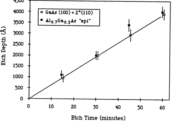
As was described in the previous section, etch rates are reported here as measured etch depths divided by etching time. Etch rates reported in this fashion are valid only if the etch rate is known to be constant with time. This assumption was tested by performing a set of experiments where etched depths were measured for different etch times at otherwise identical reaction conditions. The results of these experiments are shown in Figure 3.4 which shows etched depth as a function of etch time for both GaAs (100) + 20(011) substrates and OMVPE grown A10.7Ga0.3As epilayers etched at 4800C with 1.5
mol% CH3I in 2100 sccm hydrogen (yCH3I = 0.015). This figure clearly
shows that etched depth is linear with time, verifying that etch rate is a constant, independent of time. Having confirmed the validity of this method for etch rate determination, the etch rate of GaAs (100) + 20(011) was measured as a function of susceptor temperature, CH3I
inlet mole fraction (YCH 3I), total gas flow rate, and, for AlxGal-xAs,
aluminum fraction (x).
Figure 3.5 is an Arrhenius plot showing the temperature dependence of the GaAs (100) + 20(011) etch rate at three concentrations of CH3I;
YCH3I = 0.015, 0.0058, and 0.0012. For all of these experiments, the
carrier gas was 2100 sccm hydrogen. The lines shown in this plot were calculated using least squares analysis and the calculated slopes
4500 4000 3500
3000
a 2500 S 2000 m 1500 1000 500 0 0 10 20 30 40 50 60Etch Time (minutes)
Figure 3.4: GaAs etch depth as a function of CH3I exposure time, T =
4800C, YCH
T(°C) 105 0<
e]
Q, 103 102 10 600 550 500 450 1.1 1.2 1.3 1.4 400 1.5 1/T(K) x 1000Figure 3.5: Arrhenius diagram illustrating etch rate as a function of temperature at 3 different CH3I concentrations. YCH3I = 0.0012 (solid
correspond to activation energies of 43 (YCH3I = 0.015), 45 (YCH3I = 0.0060), and 47 (YCH31 = 0.0012) kcal/mol. Several experiments were also performed with YCH3I = 0.025 in 2100 sccm of helium and the activation energy was again found to be 43 kcal/mol. Although the activation energy did not depend on the carrier gas used, absolute etch rates in a helium carrier were roughly 1.5 times lower than for a hydrogen carrier gas under the same conditions of temperature, flow rate and YCH3I.
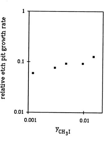
The effect of changing the inlet concentration of CH31 (YCH 3I) on the
etch rate of GaAs (100) + 20(011) substrates was studied at 4
susceptor temperatures, 4800C, 5000C, 5250C, and 5500C. The results
are shown in Figure 3.6. From this data, a reaction order (n) in inlet CH3I was determined by a least squares fit of the data to an assumed rate expression of the form:
etch rate = constant (YCH31)n (3.2)
The reaction orders thus determined were 0.84 (4800C), 0.83 (5000C),
0.80 (5250C), and 0.68 (5500C). The computed lines corresponding to
these reaction orders are also shown in Figure 3.6.
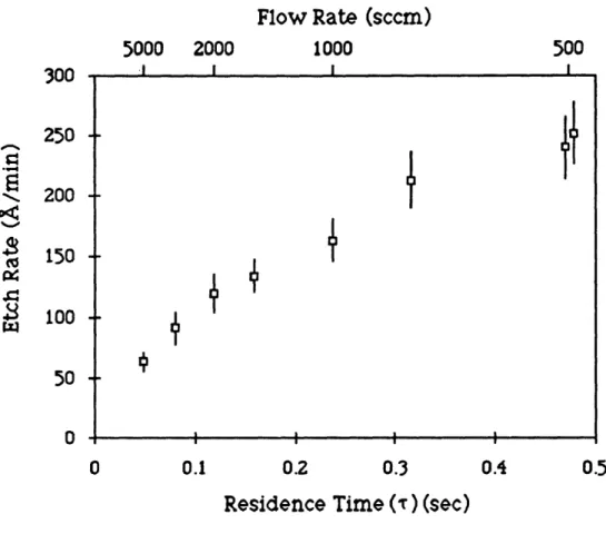
The effect of varying the total gas flow on etch rate was studied on GaAs (100) + 20(011) substrates. In these experiments, the etch temperature was a constant 4920C, yCH
3I was held constant at 0.015,
and the carrier gas was hydrogen with a total flow that was varied between 500 to 5000 sccm. The results of these experiment are
'• 13 10
(a
S 10
0.001 0.01 0.1YCH
3I
Figure 3.6: Etch rate dependence on YCH3I. Etch temperatures: 4800C
(filled squares), 5000C (open squares), 5250C (diamonds), 5500C
Flow Rate (sccm) 1000
I
0.2 0.3
Residence Time (T) (sec)
Figure 3.7: Effect of reactor gas residence time (r) on etch rate of GaAs. Etch temperature 4920C, YCH3 = 0.015.
5000 2000 300 250 500 200 150 100 LI
+
+
K~I 0.1 0.4 0.5-200 2 4) 150 -100 - 50-0.25 0 0.5 0.75 AlAs fraction (x)
Figure 3.8: Etch rate of AlxGa l-xAs samples as a function of x. Etch
conditions, 4800C, YCH31 = 0.015, and H2 flow = 2100 sccm.
U U 0
plotted in Figure 3.7 which shows etch rate as a function of the
reactor gas residence time, r (r . 1/(flow rate)).
Finally, the effect of aluminum content (x) on the etch rate of OMVPE deposited AlxGal-xAs was examined at an etch temperature of 4800C and YCH 3I = 0.015. These results are shown in Figure 3.8 which
clearly shows the etch rate to be independent of aluminum content (x) for all values studied (maximum of 0.7).
It is now of interest to properly classify the CH3I vapor etch of GaAs
based on the experimental results presented in this section. Vapor phase processes which result in a surface observable effect such as growth or etching are known to operate under a variety of rate limiting factors. These factors are generally grouped into one of two categories, vapor phase mass transport limitations and chemical kinetic limitations. Gas phase mass transport limitations will be encountered when surface reactivities are high relative to gas phase diffusion processes, this situation being characterized by the surface Dahmkohler number (DaII) >>1. Experimentally, the observed
temperature dependence of mass transport rate limited processes will be small, observed activation energies < 10 kcal/mol.
Additionally, raising the gas flow rate in mass transport controlled processes will result in increased rates due to the associated decrease in the diffusion boundary layer thickness. This effect has been
In contrast to mass transport control, kinetic controlled processes are characterized by high activation energies (> 10 kcal/mol). From the observed activation energy (43 - 47 kcal/mol), it is clear that CH3I
vapor etching is kinetically controlled over the temperature range studied. The nature of this kinetic control becomes clearer when all of the data presented in this section are considered.
The general classification of kinetic control itself tells little about the nature of the rate limiting kinetics, ie. surface or gas phase. Such distinctions can be drawn through additional experimental analysis. One of the more revealing experiments is the effect of varying gas flow rate on the etch rate at a fixed wafer position (Figure 3.7). If surface kinetic processes are solely rate limiting, then the altering of gas phase reaction conditions would have no effect on the rate. Since an effect of flow rate is observed, the main kinetic limitation is in the gas phase. A good candidate for the rate limiting reaction is the
unimolecular decomposition of CH3I to CH3 and I; the reported
activation energy for this reaction is 42.5 kcal/mol (Saito, et al, 1980), close to our measured global activation energy of 43 - 47 kcal/mol (Figure 3.5). This contention is further supported by the observed reaction order being close to 1.0 for temperatures at or below 5250C (Figure 3.6) and by the fact that AlxGal-xAs and GaAs
show no differences in etch rate at 4800C (Figure 3.8).
The data in Figure 3.7 is linear in residence time for the higher flow rates (>2000 sccm, r<0.12), consistent with a plug flow reactor
observed at higher residence times (lower gas flow velocities). At these conditions, an additional resistance appears which is likely due to an increase in the vapor phase mass transfer resistance acting in
series with the gas phase decomposition resistance. The onset of an additional mixed regime may also be occuring at higher
temperatures; at 5500C the reaction order in CH
3I is seen to drop to
0.63, suggesting that surface saturation kinetic resistances are acting in series with the gas phase decomposition resistance. Only a limited amount of data was gathered at higher etch temperatures, precluding further speculation on the nature of these surface kinetic effects.
3.3.2 Etching in the Horizontal Reactor - Surface Morphology
One of the most technologically important characteristics of an etch process is that the resulting surface morphology is featureless and specular. A major objective in development of CH3I vapor etching of
GaAs was, therefore, to determine conditions under which etched surfaces of GaAs remained smooth. Two factors were found to contribute to the etched surface morphology, the initial state of the surface (prior to loading into the reactor) and the etch conditions. The initial surface state was reproducibly controlled throughout these experiments in order to isolate the effects that reaction conditions have on etched surface morphology.