HAL Id: hal-01176845
https://hal.inria.fr/hal-01176845
Submitted on 16 Jul 2015
HAL is a multi-disciplinary open access
archive for the deposit and dissemination of
sci-entific research documents, whether they are
pub-lished or not. The documents may come from
teaching and research institutions in France or
abroad, or from public or private research centers.
L’archive ouverte pluridisciplinaire HAL, est
destinée au dépôt et à la diffusion de documents
scientifiques de niveau recherche, publiés ou non,
émanant des établissements d’enseignement et de
recherche français ou étrangers, des laboratoires
publics ou privés.
Asynchronous Charge Sharing Power Consistent
Montgomery Multiplier
Jiaoyan Chen, Arnaud Tisserand, Emanuel Popovici, Sorin Cotofana
To cite this version:
Jiaoyan Chen, Arnaud Tisserand, Emanuel Popovici, Sorin Cotofana. Asynchronous Charge Sharing
Power Consistent Montgomery Multiplier. ASYNC: 21st IEEE International Symposium on
Asyn-chronous Circuits and Systems, May 2015, Mountain View, Silicon Valley California, United States.
�hal-01176845�
Asynchronous Charge Sharing Power Consistent
Montgomery Multiplier
Jiaoyan Chen
#1, Arnaud Tisserand
#2, Emanuel Popovici
#3, Sorin Cotofana
#1Department of Computer Engineering, TU Delft, Delft, the Netherlands
#1CNRS, IRISA, INRIA, Univ. Rennes 1, Lannion, France
#2Department of Electrical and Electronic Engineering, University College Cork, Cork, Ireland
#3Abstract—A significant number of cryptographic
architectures rely on the efficient and resilient implementation of the Montgomery modular multiplier. One of the most used attacks on cryptographic implementations is based on Differential Power Analysis (DPA) or one of its variants. In this paper, a specially adjusted Latch-less Asynchronous Charge Sharing Logic (LACSL) is developed to inherently defend such architecture against DPA attacks. The proposed logic provides input data independent low-power/energy consumption which is attributed to interleaved charge sharing stages with non-static elements involved in the data path. A 32-bit LACSL Montgomery Multiplier (case study) is extensively tested through HSPICE simulations and great consistency in power/energy consumption is achieved. The normalized energy deviation and normalized standard deviation are only 0.048 and 0.011, respectively. Compared with the original ACSL implementation, besides the impressive energy coherence, 42% energy saving is demonstrated plus that the leakage power is 3.5 times smaller. Furthermore, the scalability of the proposed multiplier is explored where 64-bit, 128-bit and 256-bit designs are implemented. Again, great energy consistency is found with the highest deviation being 0.5%. The proposed techniques can be easily migrated to other low-power circuits for which accurate power/energy models can be built, independent of the input data profile.
Keywords—asynchronous; modular arithmetic; charge sharing logic; side channel attack; input data independent energy circuits
I. INTRODUCTION
Embedded cryptographic systems must be protected against Side Channel Attacks (SCAs). These attacks exploit correlations between data manipulated inside the chip (e.g., secret keys) and externally measured parameters such as computation timing [1], power consumption [2], or electro-magnetic radiations [3]. In this paper, we focus on power/energy consumption because only low-cost equipment is required to attack embedded cryptographic systems such as smart-cards. Several types of power attacks exist: Simple Power Analysis (SPA) exploits one or a few traces while DPA [2] uses statistical techniques over a large set of recorded traces. DPA, and its numerous variants, is considered as an important threat for symmetric as well as for asymmetric cryptography implementations in embedded systems.
Many SCAs against Elliptic Curve Cryptography (ECC) implementations have been proposed (see [4] for a survey). In the same time, various protections schemes, or counter-measures, have been adapted or proposed for ECC [5]. Various
uniformization schemes have been proposed for ECC: uniform formulas, regular scalar multiplication algorithms (e.g., double-and-add-always, Montgomery ladder [6], addition chains [7], etc.). Most of those protections behave at the curve operations level.
Montgomery algorithm [8] is one of the most popular
modular multiplication method both for GF(2m) and GF(p)
finite fields (ECC) and integers (RSA). Thereby the multiplier based on this algorithm serves as the kernel of these cryptosystems, called the Montgomery Multiplier (MM). Numerous hardware MMs have been proposed in [9], [10], which are designed for low-power consumption. Several FPGA implementations can be found in [11], [12], [13]. However, none of them exhibits the data independent power/energy consumption property.
In multipliers, internal data transitions (both complete ones as well as glitches) strongly impact the instantaneous power of the unit (see [14] for activity evaluation in general hardware multipliers). This dependency between the manipulated data and power profile makes the circuits vulnerable to DPA. Multiplier algorithms and architectures can be modified to remove this dependency. In [15], several algorithmic and architecture-level modifications have been proposed to design
more secure GF(2m) multipliers for ECC.
In [16] and [17], a novel CMOS logic and a dynamic look-up table technique have been proposed to address the challenge of data dependent power consumption but their utilization is limited relatively small circuits, i.e., 3 states detector circuit, S-boxes, etc.. However, there is no glitch occurrence in their implementations.
Asynchronous logic can be used at the circuit level to suppress (or at least significantly reduce) this dependency (ideally no glitches). In [18] an asynchronous interleaved multiplier based unit is proposed. In [1] an asynchronous wave pipeline implementation of an ECC processor based on the Massey-Omura multiplier is proposed. But these two designs mainly focus on the performance level rather than on data security and no power/energy results are reported.
In this paper, we investigate a circuit-level protection for modular multiplication units based on Montgomery algorithm for ECC applications (but it can also be easily adapted to RSA). The proposed MM is based on an adjusted version Asynchronous Charge Sharing Logic (ACSL), called Latch-less ACSL (LACSL) which successfully eliminates the latch
utilization between adjacent stages. In doing so, 40% lower than standard ACSL power consumption is achieved. Moreover, thanks to the exclusion of latches, our MM is more robust against DPA with Normalized Energy Deviation (NED)=0.048 and Normalized Standard Deviation (NSD)=0.011. We note that the proposed solution is not a complete countermeasure against DPA but it provides a circuit level protection scheme to increase the ECC security in embedded applications. While most of the protection work is at the curve operation level, we deal with finite field arithmetic level as a first layer of protection on top of which secure scalar multiplication algorithms can be used with a decreased cost.
The paper is organized in the following structure. In Section II, ACSL background is given, and LACSL is proposed. The MM based on LACSL is explained in Section III. The implementation results are discussed in Section IV and the paper is concluded in Section V with some future works.
II. LATCH-LESS ASYNCHRONOUS CHARGE SHARING LOGIC
In this section, first the general introduction of ACSL is briefed, such as the basic function block, and operation flow. Then, the proposed LACSL is discussed along with the comparisons with the original ACSL.
A. Background of Asynchronous Charge Sharing Logic
Asynchronous Charge Sharing Logic [19] is an asynchronous logic family that relies on charge sharing techniques to reduce the power consumption. ACSL uses adiabatic gate designs but does not require the power-clock to operate in an adiabatic fashion [20] and thus it is not itself an adiabatic logic family. Adiabatic logic aims to achieve the low power consumption by turning on and off the transistors slowly, which results in considerably small current through the transistors. Instead ACSL recovers energy from each stage through charge sharing. This has several advantages, such as exclusion of inductors and asynchronous operation. While ACSL does not provide the theoretical power saving potential of adiabatic logic, in practice it achieves similar savings. In average, ACSL saves 40% to 50% power over straight dynamic logic (requiring pre-charging), while adiabatic operation saves 50% to 60%. ACSL is based on the Positive Feedback Adiabatic Logic (PFAL) [21], building upon its gate
structure depicted in Figure 1. The PFAL (also ACSL) gate
consists of two cross-coupled inverters with a NMOS pull-up network in parallel with the inverter PMOS on the true side and a complementary NMOS network on the inverse output side. Evaluation is carried out through the Voltage Power-Clock (VPC), which is zero when the circuit is idle. As the VPC is raised the NMOS pull-up tree will set one output of the gate. As the VPC rises, the inverter network will hold the opposite side low and maintain the upward pull-on the set side. The attractiveness of ACSL resides in the fact that the drawbacks of variability associated with charge sharing logic are compensated by the asynchronous logic properties.
ACSL has been proved for its low-power characteristic in both dynamic and static aspects over other asynchronous logic families thanks to integrating charge-sharing technology with
Figure 1. PFAL function block schematic.
(a)
(b)
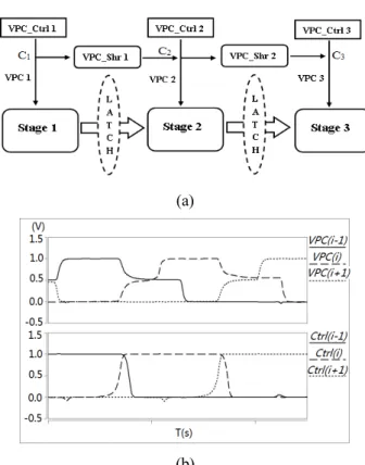
Figure 2. ACSL operation flow (a) and signal transition diagrams (b).
power gating technique [19]. The operation flow and signal
transition diagrams of three stages are depicted in Figure 2. It
can be seen that ACSL operates in a pipelined fashion utilizing handshaking protocol. The units related to VPCs are the cornerstone of ACSL. The Ctrl signals trigger the change of
VPCs while VPCs also served as completion detection signals.
Detailed explanation can be found in [19]. With balanced capacitive distribution of the architecture, high energy transfer efficiency and great power consumption consistency can also been achieved.
B. Latch-less Asynchronous Charge Sharing Logic
Due to the static storage element involved between each evaluation logic stage in ACSL, the power consistency of the whole system has to be compromised. To defend against DPA attacks, it is crucial to adjust ACSL by eliminating those static units and therefore to avoid leakage of information from power
Figure 3. Block diagram of latch-less ACSL.
Figure 4. ACSL handshaking protocol.
inconsistency. One possible way is to substitute the static latch with a dual-rail dynamic latch. Unfortunately, the subsequent high power/energy consumption is thereby inevitable. On the other hand, it is not practical to exclude the storage elements directly either, as this would deteriorate the ACSL stability. Without data retention devices, once the charge sharing finishes, the input data for the next stage might not be valid
(only at half VDD), the consequent unequal voltage distribution
not only slowing down the evaluation speed but also leading to possible error occurrences like the write error in SRAM cells.
To tackle this problem, interleaved charge sharing is considered because it could intuitively solve the unbalanced voltage situation discussed above. Figure 3 displays the block diagram of the LACSL. It can be seen that Voltage Power Clocks (VPCi, i=1..4) now handshake with at least one isolation stage rather than communicate directly between two
adjacent stages as that in Figure 2(a).By doing this, input data
for each stage is always fully charged during the computation. Moreover, it brings other improvements in terms of performance, area and power consumption as will be presented in next section. The main adjustment needed in LACSL is to re-design the VPC-CTRL circuit to maintain the power-up situation across the stages with minimum overhead. The logic units as well as VPC-SHR maintain the same designs as those in [19]. It is worth mentioning that the control signals of LACSL are the same as those in standard ACSL despite of the updates on VPCs. For the conventional ACSL, the control signal of an individual stage is only valid when the control signals of two adjacent stages are low. The signal transition diagram of ACSL handshaking protocol is illustrated in Fig.4.
III. MONTGOMERY MULTIPLIER BASED ON LACSL
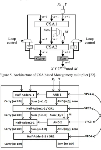
Efficient and resilient implementation of the Montgomery modular multiplier is well desired in a significant number of cryptographic architectures. There are various designs of modular Montgomery multiplier introduced in [11-15]. The Carry Save Adder (CSA) based Montgomery modular multiplier is a popular alternative well known for its high throughput. In [22], an efficient CSA architecture for
Montgomery multiplier depicted in Figure 5is proposed where
X,Y and M are the multiplicand, the multiplier and the modulus,
respectively and let n be the number of digits in their binary representation. The modulus M needs to be relatively prime to the radix, i.e. there exists no common divisor for M and the radix. The multiplicand and the multiplier need to be smaller than M.
The main feature of this design is that it utilizes only two
CSA arrays to carry out computation through iterations. The
re-use of those two CSAs is the key operation where shift registers are necessary. The data-independent power consumption could be realized once each iteration/loop consumes the same amount of power, which could be significant for keeping the information safe from a DPA attack. However, several modifications on this architecture must be taken care of in order to use latch-less ACSL.
First, in Figure 5, shift registers synchronized by the loop signal are still present. On the other hand, if LACSL is applied, shift registers are then no longer essential while the same functionality can be accomplished by simple re-wiring as everything is triggered under the remits of the handshaking protocol.
Second, as it can be seen in Figure 5 the data fed into both
CSAs are from the output of AND gates and previous CSAs.
This makes the timing control somewhat more complex for LACSL as the inputs arrival time must be synchronized. To overcome this, we re-arrange the CSA, which internally are individual Full Adders (FA), into two layers. The first layer consists of the conventional Half Adders (HA) while the second layer consists of HAs and OR gates. The block diagram of the proposed CSA based architecture is presented in Figure 6. The first layer of HAs can thereby be placed at the same
level with AND gates (Xi and Y as inputs), which fixes the
initial input-data sequence problem. Now every level of data-path has only the input coming from the previous stage. Furthermore, the capacitive load is still balanced for each pair of VPC sharing stage (VPC1↔VPC3; VPC2↔VPC4) although two neighboring stages have different load (size of circuits).
Thus far, all necessary conditions for the realization of an LACSL based Montgomery multiplier have been described. As the cornerstone of the entire operation, VPC execution processes (Charging, Sharing, Discharging) are the most significant.
Figure 7 illustrates the operation flow of 4 stages LACSL. Figure 8 presents the simulation waveforms indicating the voltage changes at each stage.
It can be concluded that during the sharing of two leaping stages, the other two maintain their previous level. According to the extensive simulation, the sharing operation is swift and
steady. In next section, implementation results of LACSL MMs would be thoroughly discussed.
Figure 5. Architecture of CSA based Montgomery multiplier [22].
Figure 6. Architecture of LACSL CSA based Montgomery multiplier.
Figure 7. VPCs operation flow of LACSL.
Figure 8. Waveforms representing voltage changes at each stage.
IV. IMPLEMENTATION RESULTS
Various sizes of LACSL MMs are implemented, ranging from 32-bit to 256-bit while the 32-bit one is extensively investigated to verify its resistance against DPA. Meanwhile, a 32-bit ACSL based design is also implemented and compared in order to demonstrate the LACSL advantages, such as energy consistency and low energy characteristic. All circuits are
designed using 45nm CMOS technology, where VDD=1V,
Vthn=0.32V, Vthp= -0.31V, and simulated using HSPICE.
For the 32-bit MMs, two main tests are set-up as follows: 1) fixed X, fixed M, various Y with different Hamming weights ranging from 10 to 22, where power, delay, energy data per iteration for both LACSL and ACSL MMs are recorded (32 iterations per operand Y); 2) 100 sets of random X, fixed M, random Y where total energy during the course for the LACSL MM is obtained.
For the 64-bit, 128-bit, and 256-bit LACSL MMs, 10 iterations of random input vectors with corresponding bit-width are generated and simulated. In spite of input size doubled and redoubled, the logic depth remains the same so that the overall delay should be close if the sizes of VPC-CTRL and VPC-SHR are proportionally scaled. The main distinction is in the total number of iterations and the corresponding energy consumption, which depends on the input-width size.
A. 32-bit LACSL Montgomery Multiplier
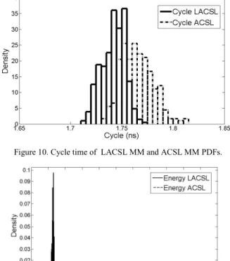
The power, delay and energy per iteration are measured. First, Figure 9 depicts the power consumption from the LACSL MM and ACSL MM in scattered fashion. It is rather consistent (around 250uW) for the LACSL design in contrast to that of the ACSL MM whose distribution is quite decentralized. It can thereby be anticipated that the energy consumption would also be constant if each iteration/cycle takes equal length of time. The Probability Density Functions (PDFs) of cycle time of LACSL and ACSL MMs are shown in Figure 10. The cycle time refers to the delay for each loop. For LACSL, it ranges from 1.72ns to 1.77ns while it is a bit larger for the ACSL counterpart. The adjustment made on LACSL improve the performance a bit rather than compromise it. The Power Delay Products (PDPs) of these two models, also regarded as energy consumption, are illustrated in Figure 11 where the high spike represents the energy of LACSL, around 450fJ. On the other hand, the energy consumption of ACSL spreads relatively widely as well as it is higher than that of LACSL.
The corresponding energy consumption data are summarized in Table I, where the minimum/maximum energy per cycle over total 416 simulated cycles is listed. In the same table, the Normalized Energy Deviation (NED) is defined as:
=
(
/
) -
(
/
)
(
/
)
Max energy cycle Min energy cycle
NED
Max energy cycle
(1)Meanwhile, SD is the standard deviation of the energy per cycle, and the Normalized Standard Deviation (NSD) is defined as:
(
/
)
SD
NSD
Mean energy cycle
=
(2)It can be easily observed that LACSL outperforms the conventional ACSL, even the MAX energy consumption of LACSL is smaller than the MIN energy consumption of ACSL. The average energy consumption reduction against ACSL is 42% in this case. Moreover, NED is reduced from 0.65 for ACSL to 0.048 for LACSL, i.e., more than 13 times. NSD shrinks from 0.29 to as little as 0.011 thanks to the elimination of static storage elements.
As mentioned at the beginning of this section, other than the data for iterations, we also collect the energy for 100 sets of random inputs over the entire calculation for the LACSL MM. The data are also summarized in Table I accordingly. The corresponding NED and NSD get further decreased by 5 and 7 times, respectively.
Additionally, leakage power for both designs in idle mode is also recorded. For the ACSL MM, it consumes 7.1µW where the LACSL counterpart only dissipates 2.05µW, nearly 3.5 times smaller. Furthermore, the transistor count for the LACSL 32-bit MM is 3912 in contrast to 5224 to the ACSL one.
As mentioned in the Introduction (Section I), the algorithm and architecture level protections proposed in [15] for secure multipliers reduce the variations of the electrical activity in the circuit. But there are still a few percent variations in the best case. On the other hand, in [16] and [17], two approaches were introduced with impressive NEDs and NSDs. In [16], the NED and NSD for a XOR gate implemented in 0.35µm CMOS
process are 0.13 and 0.05, respectively. In [17], for S7-Box
implemented in 0.12µm CMOS technology, the corresponding
NEDs and NSDs for both pre-layout and post-layout designs
are 0.0014, 0.0003, and 0.0402 and 0.0102, respectively. It should be noted that both of these two models (XOR gate and
S7-Box) are without propagation, which means there is no glitch at all. Therefore, it is difficult to directly compare them with our LACSL MMs since our design is more complicated than theirs.
Moreover, there are circuit-level techniques where dual-rail or multi-rail encoding of data are used [23]. They are dedicated to reduce current variations when the loads of all rails are
Figure 9. Scattered plots of LACSL power data and ACSL power data.
Figure 10. Cycle time of LACSL MM and ACSL MM PDFs.
Figure 11. Energy consumption of LACSL MM and ACSL MM PDFs.
balanced. Compared to our LACSL solution, these multi-rail approaches lead to considerable area overhead and require high accuracy clock distribution circuits to ensure the load balancing of all logical gates and flip-flops.
TABLE I. SUMMARY OF ENERGY DATA
32-bit MMs ACSL per cycle LACSL per cycle Operand X,Y LACSL per
MAX(fJ) 1288 439 14832 MIN(fJ) 450 418 14698 NED 0.65 0.048 0.009 SD(fJ) 215 4.7 23 Mean(fJ) 733 428 14752 NSD 0.29 0.011 0.0015 Leakage Power(µW) 7.1 2.05 2.05
TABLE II. SUMMARY OF AVERAGE POWER, DELAY, ENERGY
LACSL MMs 64-bit 128-bit 256-bit
Avg. Power (uW) 500 1046 1970
Avg. Cycle (ns) 1.9 2.0 2.1
Avg. Energy (fJ) 950 2092 4137
B. Scability of LACSL Montgomery Multiplier
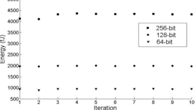
We use LFSRs to generate input vector for each LACSL MM with different bit-width to briefly explore the scalability of the proposed design. The selected bit-widths are 64-bit, 128-bit and 256-bit. Table II lists the average data of 10 iterations for these three different bit-width MMs while the average deviations are calculated. Since there is not sufficient data for statistical analysis due to the expensive simulation time and memory requirement, NED and NSD are not available. However, good LACSL scalability can be observed at first glance. The highest average deviation is 0.5% for both 64-bit and 128-bit MMs while it is only 0.3% for the 256-bit one. Energy per cycle simulation data of three LACSL MMs are plotted in Figure 12 where the consistency is clear to see.
C. Summary
The feature of explicit power consistency is embraced in the LACSL based Montgomery multipliers according to the data above which strongly shows the potential of application against DPA attacks. LACSL arithmetic operators can be used as a partial protection against side-channel attacks. In classical operators, the large power variations are used by the attacker to get strong information the time boundaries of the low-level operations (e.g., finite-field operations for ECC) and then use these information to guess what are the higher level operations (e.g., curve level operations for ECC). Using LACSL operators, this type of time references are not easily accessible anymore. It is hasty to say ACSL operators are totally protected against power analysis side-channel attacks but they significantly increase the number of traces to be collected for the DPA attacks.
V. CONCLUSIONS AND FUTURE WORK
A circuit-level protection for modular multiplication units based on the Montgomery algorithm for Elliptic Curve Cryptography applications is presented along with the proposed Latch-less Asynchronous Charge Sharing Logic. It is shown that in our implementation the power/energy consumption is independent on the input data distribution which is a great asset in safeguarding against side channel
attacks such as Differential Power Analysis. The normalized
energy deviation and normalized standard deviation are 0.048 and 0.011 respectively, remarkably lower than those of the
Figure 12. Energy consumption of different sized LACSL.
original Asynchronous Charge Sharing Logic. Over 40% energy reduction is obtained as well. Moreover, the scalability of the LACSL Montgomery Multiplier is also demonstrated by doubling and re-doubling the operand bit width where the average energy deviation is less than 0.5%. The proposed LACSL methodology can be applied to other cryptographic algorithms and architectures including RSA. However, the proposed solution is not a complete countermeasure against DPA but it provides a circuit level protection scheme to increase the security of ECC in embedded applications.
Further research and low level design will be required to analyze the impact of layout on the proposed methodology. A future work may be also the design of a complete crypto processor where arithmetic units, internal registers and control elements are all implemented using LACSL.
ACKNOWLEDGMENT
This work has been sponsored by the European Commission FP7 FET-Open iRISC (Innovative Reliable Chip Designs from Unreliable Components) project, SpiNaCH (CNRS PICS 6023) project and PAVOIS project (ANR 12 BS02 002 01).
REFERENCES
[1] O. Hauck, A. Katoch and S.A. Huss : a 0.35um CMOS 1.5 GHz Elliptic Curve Public Key Cryptosystem chip, IEEE Proc. 6th International Symposium on Asynchronous Circuits and Systems (ASYNC), Apr. 2000, pp. 188-197.
[2] S. Mangard and E. Oswald and T. Popp, Power Analysis Attacks: Revealing the Secrets of Smart Cards, Springer, 2007.
[3] K. Gandolfi and C. Mourtel and F. Olivier, Electromagnetic Analysis: Concrete Results, Proc. Cryptographic Hardware and Embedded Systems CHES, LNCS, Vol 2162, May 2001, pp. 251-261.
[4] E. Oswald, Advances in Elliptic Curve Cryptography, Cambridge University Press, Vol. 317, April 2005, pp. 69-86.
[5] M. Joye, Advances in Elliptic Curve Cryptography, Cambridge University Press, vol. 317, April 2005, pp. 87-100.
[6] P. L. Montgomery, Speeding the Pollar and Elliptic Curves Methods of Factorisation, Mathematics of Computation, Vol. 48, Jan. 1987, pp. 243-264.
[7] A. Byrne, N. Meloni, A. Tisserand, E. M. Popovici and W. P. Marnane, Comparison of Simple Power Analysis Attack Resistant Algorithms for an Elliptic Curve Cryptosystem, Journal of Computers, Vol 2, 2007, pp. 52-62.
[8] P. L. Montgomery, Modular Multiplication Without Trial Division, Mathematics of Computation, Vol. 44, Apr. 1985, pp. 519-521.
[9] S.Hee-Kwan, and S.G.Oh. Design and implementation of scalable low-power Montgomery multiplier. Computer Design: VLSI in Computers and Processors, ICCD 2004, pp.524-531..
[10] Wang, Xin, Peter Noel, and Tad Kwasniewski. Low power design techniques for a Montgomery modular multiplier. Intelligent Signal Processing and Communication Systems, ISPACS 2005,pp. 449-452. . [11] A. Daly and W. P. Marnane, Efficient Architectures for Implementing
Montgomery Modular Multiplication and RSA Modular Exponentiation on Reconfigurable Logic, Proc. 10th International Symposium on Field Programmable Gate Arrays (FPGA), ACM, Feb. 2002, pp. 40-49 [12] C. McIvor, M. McLoone, M. and J.V. McCanny, FPGAMontgomery
Field-Programmable Custom Computing Machines (FCCM), Apr. 2004, pp. 279-282
[13] M. Hamilton and W. P. Marnane and A. Tisserand, A Comparison on FPGA of Modular Multipliers Suitable for Elliptic Curve Cryptography over GF(p) for Specific p Values, Proc. 21st International Conference on Field Programmable Logic and Applications (FPL), IEEE, Sept. 2011, pp. 273-276.
[14] A. Tisserand, Fast and Accurate Activity Evaluation in Multipliers, Proc. 42nd Asilomar Conference on Signals, Systems and Computers, IEEE, Oct. 2008, pp. 757-781.
[15] D. Pamula and A. Tisserand, GF(2^m) Finite-Field Multipliers with Reduced Activity Variations, 4th International Workshop on the Arithmetic of Finite Fields, LNCS, Vol. 7369, July 2012, pp. 152-167. [16] A. Manfred, S. Mangard, R. Menicocci, N. Olivieri, G. Scotti, and A.
Trifiletti. A novel CMOS logic style with data independent power consumption. IEEE International Symposium on Circuits and Systems, 2005., pp. 1066-1069.
[17] M. Bucci, L. Giancane, R. Luzzi, and A. Trifiletti, A dynamic and differential CMOS lookup table with data independent power consumption for cryptographic applications on chip cards. IEEE
Transactions on Dependable and Secure Computing, , 4(4), 2007, pp. 245-251.
[18] M. Feldhofer, T. Trathnigg, and B. Schnitzer, A Self-Timed Arithmetic Unit for Elliptic Curve Cryptography, Proc. Euromicro Conference on Digital System Design (DSD), IEEE, Sept. 2002, pp. 347-350. [19] J. Chen, D. Vasudevan, M. Schellekens, E. Popovici, Ultra Low Power
Asynchronous Charge Sharing Logic, Journal of Low Power Electronics, Vol. 8, No. 4, August 2012, pp. 526-534.
[20] M. Yong and D.K. Jeong, An efficient charge recovery logic circuit. IEICE transactions on electronics, 1996. 79(7): p. 925-933.
[21] A. Vetuli, S. Pascoli, and L. Reyneri, Positive feedback in adiabatic logic. Electronics Letters, 1996. 32(20): p. 1867-1869.
[22] Y-Y. Zhang, Z. Li, L. Yang, S-W. Zhang, An efficient CSA architecture for Montgomery modular multiplication, Microprocessors and Microsystems, Volume 31, Issue 7, 1 November 2007, pp. 456-459. [23] S. Guilley, L. Sauvage, F. Flament, V.V. Hoogvorst, R.P. Pacalet,
Evaluation of Power Constant Dual-Rail Logics Countermeasures against DPA with Design Time Secutirty Metrics, IEEE Transactions on Computers, 2010, Vol.59, No.9, pp.1250-1263.