Carbon Nanotube Interconnects for IC Chips
byHashina Parveen Anwar Ali Bachelor of Engineering (Electrical) National University of Singapore, 2005
MASSACHUS•-.I INM , OF TECHNOLOGY
OCT 0 2 2006
LIBRARIES
SUBMITTED TO THE DEPARTMENT OF MATERIALS SCIENCE AND ENGINEERING IN PARTIAL FULFILLMENT OF THE REQUIREMENTS FOR THE
DEGREE OF
MASTER OF ENGINEERING IN MATERIALS SCIENCE AND ENGINEERING AT THE
MASSACHUSETTS INSTITUTE OF TECHNOLOGY September 2006
C 2006 Hashina Parveen Anwar Ali. All Rights Reserved
The author hereby grant to MIT permission to reproduce and to distribute publicly paper and electronic copies of this thesis document in whole or in part in any medium or hereafter
created,
Signature of Author...
Department of Materials Science and Engineering August 8, 2006
Certified by ... . •... ... Carl V. Thompson Stavros Salapatas Professor of Materials Science and Engineering Thesis Supervisor
Accepted by ... .. ./ ... ... ... ....
Samuel M. Allen POSCO Professor of Physical Metallurgy Chair, Departmental Committee on Graduate Students
Carbon Nanotube Interconnects for IC chips
by
Hashina Parveen Anwar Ali
Submitted to the Department of Materials Science and Engineering on August 8, 2006 in Partial Fulfillment of the
Requirements for the Degree of Master of Engineering in Materials Science and Engineering
ABSTRACT
Carbon nanotubes (CNTs) have been investigated as candidate materials to replace or augment the existing copper-based technologies as interconnects for Integrated Circuit (IC) chips. Being ballistic conductors, CNTs are capable of carrying higher current densities of up to 101oA/cm2 and high thermal conductivity. This thesis examines the technological aspect of carbon nanotubes - how these tubes can excel in place of copper in terms of their performance and integration into the current commercial IC chip process. A detailed literature review is covered, together with a performance analysis of the resistances between copper and CNT interconnects. Further, a business model is proposed on the possibility of introducing this technology into the mainstream IC industry.
Thesis Supervisor: Carl V. Thompson
Acknowledgements
I cannot fully express my profound gratitude to several exceptional people who guided, critiqued and encouraged me through the conception, development and conclusion of my M.Eng thesis dissertation.
First and foremost, I thank my MIT professor, Stavros Salapatas Prof Carl. V. Thompson for agreeing to be my supervisor for a forefront project scope and his superb guidance. An understanding supervisor and firm one, he ensured that I went on with my project within the boundaries set by him and helped me whenever I was faced with challenges.
My NTU facilitator Prof Zhang Qing has been a great help here in Singapore, keeping his doors open for me to come in anytime and answered any doubts I have on carbon nanotubes.
The Nanotubes research group at MIT under Prof Thompson has been the team that guided me through my research on carbon nanotubes. In particular, I sought the help of Gilbert Nessim, who has provided me with his experience and expertise. Thanks a lot!
Last, but not the least, my family and friends who have supported and cheered me up to push forward with enthusiasm and vigor to complete this M.Eng dissertation successfully.
Contents
ABSTRACT ... 2 ACKNOWLEDGEMENTS ... 3 CO NTENTS ... 4 LIST OF FIGURES ... 5 LIST OF TABLES ... 5 ABBREVIATIONS ... 8 CHAPTER 1 INTRODUCTION... 9 CHAPTER 2 FUNDAMENTALS ... 152.1 CURRENT TECHNOLOGY - COPPER DAMASCENE PROCESS ... 15
2.2 DESIGN CONSIDERATIONS IN COPPER INTERCONNECTS ... 17
2.3 LIMITATIONS OF COPPER INTERCONNECTS - NEED FOR A NEW SOLUTION ... .... 19
2.3 PROPOSED TECHNOLOGY - CARBON NANOTUBES... ... 23
2.4 METHODS OF FABRICATING CNTS ... ... 25
2.5 PROPERTIES OF CNTS THAT ENCOURAGE ITS USE AS POSSIBLE INTERCONNECTS ... 28
2.6 OTHER REMARKABLE PROPERTIES OF CNTS ... ... 34
CHAPTER 3 CARBON NANOTUBES AS INTERCONNECTS... ... 36
3.1 FABRICATION OF CNT INTERCONNECTS ... 36
3.2 DESIGN CONSIDERATIONS FOR CNT INTERCONNECTS ... 39
3.2.1 Research on SWNT bundles as Interconnects ... ... 39
3.2.2 Research on MWNTs as Interconnects ... ... 44
3.2.3 Patented Designs using CNTs... 47
3.3 RESISTANCE MODEL FOR CNTS VERSUS COPPER INTERCONNECTS ... 49
3.3.1 Assumptions - Interconnect Wire Design in IC chip ... . 50
3.3.2 Assumptions and Calculations for Copper Interconnects... 51
3.3.3 Assumptions and Calculations for CNT Interconnects ... . 53
CHAPTER 4 TECHNICAL ASSESSMENT OF CNTS AS INTERCONNECTS ... 56
4.1 FABRICATION ... ... ... 56
4.2 TREND IN THE RESISTANCE OF COPPER... 58
4.3 EFFECTS OF KEY PARAMETERS ON CNT PERFORMANCE ... 59
4.3.1 Effect of packing distance on SWNT bundle... ... 60
4.3.2 Effect of Outer Diameter on Resistance of Single MWNTs... 61
4.4 ANALYSIS ON THE MWNT MODELS ... ... 63
4.4.1 Comparison of Single MWNT models ... ... 63
4.4.2 Effect of MWNT rings on the MWNT bundle resistance...65
4.5 OVERALL RESISTANCE TRENDS -CNTS VERSUS COPPER INTERCONNECTS... ... 66
4.5.1 Technology Node - 80nm ... 67
4.5.2 Technology N ode - 45nm ... ... 67
4.5.3 Technology Node - 14nm ... 68
4.6 RESULTS AND COMMENTS ... 68
5.1 T ECHNO LOGY SUPPLY C HAIN ... ... ... 70
5.2 INTELLECTUAL PROPERTY ... 71
5.2.1 CNT patents in general ... ... ... 72
5.2.2 Patents specific to CNT interconnects in IC chips ... 74
5.3 TARGET W ORLD M ARKET ... ... ... 76
5.3.1 Semiconductor M arket Trends ... 76
5.3.2 Forw ard Looking Trends ... 78
5.3.3 Emerging Market -Nanotechnology ... . ... 78
5.3.4 Opportunities for implementing Nanomaterials ... ... ... 80
5.3.5 Risks of implem enting N anom aterials ... 80
5.4 SOURCES OF FUNDING ... 81
5.5 INVESTMENT COSTS ... ... 84
5.6 B USIN ESS PLAN ... 86
5.6.1 Success Factors ... ... 86 5.6.2 Implementation ... ... 88 5.7 FINANCIAL VIABILITY ... 90 5.8 EXECUTION PLAN ... 90 CHAPTER 6 CONCLUSION ... 91 R EFER EN C ES ... 93
APPENDIX I SCMOS LAYOUT RULES ... 95
APPENDIX 2 FLOWCHART OF INVENTION IN US PATENT 6,933,222... 97
List of Figures
Figure 1.1: The first Integrated Circuit (IC) - Kilby's invention (left), Noyce's invention (right) ... 9Figure 1.2: Cross-section of a typical IC Chip (MPU device) showing the hierarchical scaling of the copper wires and vias (highlighted in light grey). [1] ... ... 10
Figure 1.3: A futuristic picture of a CNT via replacing Copper. (a) A hole is made in the dielectric above the metal layer to be contacted. (b) A catalyst particle is deposited or generated at the bottom of the via from which the CNT can be grown (c) [2] ... ... 13
Figure 1.4: The current situation of CNTs in vias - cross-section SEM images of vias with CVD-grown MWNTs. The catalyst particles are based on Fe and the supporting metal layer is Ta. [5]... 13
Figure 2.1: Illustration of the copper damascene process [4] ... 16
Figure 2.2: Interconnect scaling scenarios for (a) fixed metal height and (b) fixed metal aspect ratio [33] ... ... ... 18
Figure 2.3 Trend in Cu resistivity [1] ... ... 19
Figure 2.4: Dual Damascene Integration Concerns [33] ... 20
Figure 2.5: Maximum allowed RMS current densities for local vias under self-consistent Joule heating and EM lifetim e constraints [32] ... ... ... ... ... 22
Figure 2.6: Atomic configuration of (a) armchair (n, n), (b) zigzag (n, 0), and (c) general (inm, n) CNTs. ... . . . . .... 23
Figure 2.7: Indexing scheme for a SWNT in terms of integer pair (m, n) ... 23
Figure 2.8 Density of States for a metallic and semiconducting tube ... ... 24
Figure 2.9: Carbon Arc experimental setup for CNT synthesis [8] ... ... 25
Figure 2.10: Laser Vaporization Method [8] ... ... 26
Figure 2.11: CVD method schematically shown by Wagner et al [9] ... 27
Figure 2.13: Calculations on the packaging density of a dense (x = d) SWNT bundle [17] ... 31
Figure 2.14: Number of conduction channels per graphene shell versus shell diameter for metallic and semiconductor shells. The average number of conduction channels is also plotted assuming that statistically one-third of the shells are metallic. [22] ... 32
Figure 2.15: A graph of the thermal conductivities of iron, silver and diamond [24] ... 34
Figure 2.16: Thermal Conductivity of (10,10) CNT as a function of temperature [11 ] ... 34
Figure 3.1: Schematic of the Li group's Bottom up approach process [13] ... 37
Figure 3.2: Schematic of the buried catalyst approach by the Nihel group[14] ... 37
Figure 3.3 Equivalent circuit model for an isolated SWNT, length less than the mean free path of electrons, assum ing ideal contacts [15] ... 40
Figure 3.4: Schematic of CNT-bundle interconnect. Elements labeled with numbers are the ones characterizing the electrostatic coupling capacitance of the CNTs along the edges of the bundle. Each circular cross-section CNT is shown along with the circumscribing square conductor. CED, and CEf are the intrinsic plate capacitances. [39] ... ... ... 41
Figure 3.5: AC circuit model for interacting electrons in a carbon nanotube [15] ... 42
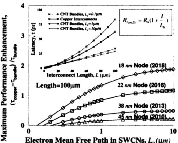
Figure 3.6: Inset: Latency versus interconnect length for minimum-sized copper wires implemented at the 22nm node and bundles of SWNTs with electron mean-free paths of 0.1, 1 and 10 Om, assuming that SWNT resistance increases linearly with length. Main plot: Maximum performance enhancement that can be achieved by using CNTs versus electron mean-free path in nanotubes for four various technology nodes. [38] ... 43
Figure 3.7: Maximum interconnect temperature rise for Cu interconnects and vias versus CNT bundle vias integrated with Cu interconnects [17]. For CNT bundles, the shaded region shows the range 1750W/mK < Kth < 5800W/mK. Reference (substrate) temperature = 378K. [17] ... 44
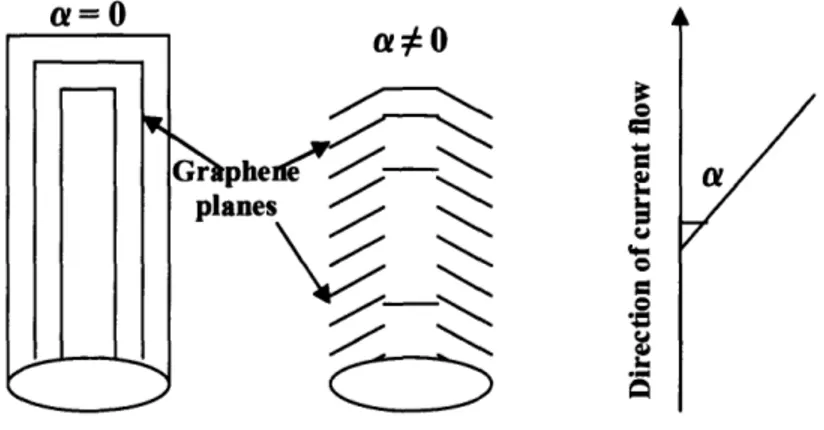
Figure 3.8: Factors influencing CNT resistivity: no. of shells and orientation of the graphene planes. [5] ... ... ... ... ... 45
Figure 3.9: Dependence of the total resistance of CNT vias on the number of CNTs [42] ... . 46
Figure 3.10: XRD patterns of MWNTs/Co/Ti samples (a) Co(2.5nm)/Ti(6nm) (b) Co(lnm)/Ti(2nm). Cross-sectional view of MWNTs/Co/Ti/Ta/Cu bottom layer structures (c) Co(2nm)/Ti(6nm) (d) Co(Inm)/Ti(2nm) MWNTs with Co nanoclusters inside the ends of the nanoclusters inside the ends of the nanotubes grew vertically on the Ti contact layers. [43] ... 47
Figure 3.11 Cross-sectional view of semiconductor device; CNTs in vias are labeled as 42 and Cu in vias are labeled as 34 [24] ... ... ... ... .. ... ... 48
Figure 3.12 Sectional view of two stages of fabrication of CNT ICs using CNTs (labeled as 152) [25] ... ... 49
Figure 3.13: Cross-section of Square Vias with design rule specifications (On left, CNT, right, Cu via). The shaded area is to account for Cu barrier thickness ... ... 50
Figure 3.14: Cross-section of Circular Vias when manufactured (On left, CNT, right, Cu via) The shaded area is to account for Cu barrier thickness ... 51
Figure 3.15: A one-tier metal layout view of a via between 2 metal layers. The dimensions given are assumed for the resistance model ... 51
Figure 4.1: Resistance of Copper (from 80nm to 45nm) (Sq: Square area, Cir: Circular area)... 58
Figure 4.2: Resistance of Copper (from 45nm to 14nm) (Sq: Square area, Cir: Circular area)... 59
Figure 4.3: Resistance of tube (RL) versus the Packing distance between 2 SWNTs (Each SW NT: Diameter Inm and length of I tm) ... ... 60
Figure 4.4: Resistance of tube (RL) versus the Packing Distance between 2 MWNTs (Each MWNT: Diameter 5nm, Diameter Ratio 0.35 and length of 1 tm) ... 61
Figure 4.5: Resistance of tube (R.) versus Outer MWNT Diameter with different Diameter Ratios of 0.35, 0.65 and 0.8. (Each MWNT: length of l tm and conductance of 2Go in each ring (General model) ) ... ... 62
Figure 4.6: Comparison of Single MWNT calculations, 80nm on left, 45nm on right... 63
Figure 4.8: Resistance of MWNT bundle versus number of rings in each MWNT at 14nm technology
node (Each MWNT: Diameter 5nm, Diameter ratio 0.35 and length of l• m) ... 65
Figure 4.9: Overall resistance trends for 80nm node (Left: for vias, Right: for long interconnects)... 67
Figure 4.10: Overall resistance trends for 45nm node (Left: for vias, Right: for long interconnects). 67 Figure 4.11: Overall resistance trends for 14nm node (Left: for vias, Right: for long interconnects). 68 Figure 5.1: A typical Silicon wafer manufacturing process chain ... 70
Figure 5.2: US patents or published applications referring to carbon nanotubes in the patent abstract (1999 - 2004) [23] ... .. ... ... . ... 72
Figure 5.3: Carbon nanotube patents issued by US PTO, from 1999-2004 (the data was collected on 04/25/2005) [23] ... ... ... ... ... ... ... 72
Figure 5.4 Sectional view of a semiconductor device that only uses CNTs (lines in diagram) from Fujitsu Patent [24]... ... ... ... . ... ... ... 75
Figure 5.5: W orldwide Semiconductor Trends [34] ... .... ... 76
Figure 5.6: Worldwide Semiconductor Consumption highlighting the change in consumption from majority N. America in 2000 to ROW in 2005. ROW includes Asia Pacific regions such as China, Taiwan, Singapore, Korea etc [34] ... ... 77
Figure 5.7: Global Nanoelectronics Market Forecast [36] ... 79
Figure 5.8: Global Market and Forecast for Nanomaterials (SEMI 2005) [36] ... 79
Figure 5.9: Graphs showing rising costs of starting a fab [30] ... 85
Figure 6.1 : Summary of the considerations for a successful IP business model ... 92
List of Tables
Table 1.1: MPU Interconnect Technology Requirements - Long-term years [1]... 12Table 1.2: Comparison of different interconnect solutions [6] ... ... 12
Table 2.1: Dielectric constants for several low-k materials... 17
Table 2.2: MPU Interconnect Technology Requirements - Long-term years [1]... 21
Table 2.3: Most important properties of metallic carbon nanotubes ... ... 34
Table 2.4: Comparison of CNT with some of the toughest materials [10] ... 35
Table 2.5: Quick Facts about Carbon Nanotubes [10] ... 35
Table 3.1: Specifications for copper at different technology nodes [1] ... ... 52
Table 4.1: Comparison of the fabrication process... 56
Table 4.2: Calculated values of a fixed diameter ratio of 0.35 to determine effect of outer diameter on resistance for a single MWNT ... ... 62
Table 4.3: The constants used to calculate the resistance of copper [1] ... 66
Table 5.1: Carbon nanotube patents issued by US PTO, from 1999-2004 (the data was collected on 25 April 2005) [23] ... 73
Abbreviations
CMP - Chemical Vapor Deposition
CNT - Carbon Nanotube
CVD - Chemical Vapor Deposition
EM - Electromigration (Lifetime)
EUVL - Extreme Ultra Violet Lithography
HFCVD - Hot Filament Chemical Vapor Deposition
IC - Integrated Circuit
IMD - Inter-metal dielectric
ITRS - International Technology Roadmap for Semiconductors
MARCO - Microelectronics Advanced Research Corporation
MPU - Multiprocessor Unit
MTF - Median Time to Failure
MWNT - Multi-wall Carbon Nanotube
OEM - Original Equipment Manufacturer
PECVD - Plasma Enhanced Chemical Vapor Deposition
RC - Resistance-Capacitance (in terms of time delay)
SEM - Scanned Electron Microscope
SPM - Scanning Probe Microscope
SWNT - Single-wall Carbon Nanotube
Chapter I Introduction
The first integrated circuit (IC) developed by Jack Kilby of Texas Instruments and Robert Noyce of Fairchild semiconductor in 1958 triggered the growth of semiconductor industries that lead to the popularity of miniature devices for everyday use. Three general strategies have guided these advances: i) scaling down minimum feature size, ii) increasing die size, and iii) enhancing packing efficiency (i.e. increasing the number of transistors that can fit into an IC). Mass production of integrated circuits, their reliability, low cost and ease of adding complexity, prompted the use of standardized ICs. This resulted in the dominance of IC chips in various applications ranging from computers to cellular phones to digital microwave ovens.
I
SEP•Z L A 1.6 1 Lle A W lliR 3t I IILJ Cl CU l LlL 1L) -- l zIIUp a ti
Robert Noyce was ingenious to consider depositing metal lines by direct vacuum evaporation of aluminum [29] to link up key components on a silicon wafer thus the interconnect was born. The function of an interconnect is to distribute clock and other signals and to provide power and ground lines to the various circuits / system functions on a chip. The fundamental
characteristic of an interconnect is to meet the high-speed transmission needs of chips in proportion to the scaling of feature sizes.
Currently in the industry, Copper is being used as interconnect material in the manufacture of IC chips at the 0.13pm technology node. Figure 1.2 shows a cross-sectional view of a typical IC chip where the light gray areas indicate the metallic wires. The bottommost layer consists of various p-n junction transistor devices. The subsequent layers above hold the different local (Metal 1), intermediate and global power lines and clock signals, connecting one device to another. Each metal wire is surrounded by a dielectric (usually SiO2), preventing short circuits and minimizing interference between signals as much as possible. Vias are included to provide connections of metallic wires between two different layers.
Global
Intermediate
Metal I
Passivation
Dielectric Etch Stop Layer
• Dielectric Capping Layer
Pre-Metal Dielectric Tungsten Contact Plug
,-
Metai 1 PitchFigure 1.2: Cross-section of a typical IC Chip (MPU device) showing the hierarchical scaling of the copper wires and vias (highlighted in light grey). 11]
ICs have consistently migrated to smaller feature sizes over the years, allowing more circuitry to be packed on each chip. As the feature size shrinks, the benefits multiply: both
the cost per unit and the switching power consumption go down, and the speed goes up. While, scaling of interconnects serves to reduce cost, it increases latency (response time) in absolute value and energy dissipation relative to that of transistors. These increases are due to relatively larger average interconnect lengths (measured in gate pitches) and larger die sizes for successive generations. Further, ICs with nanometer-scale devices do have their share of problems, principal among them are leakage currents and electromigration.
As copper resistivity increases rapidly with decreasing linewidth, the reliability of interconnects becomes an issue. As more and more transistors can be packed into a single IC chip, the tiny copper interconnects are required to carry huge current densities over longer distances in order for all the transistors to work to their full capacity. This results in longer RC delays due to both line resistance and load capacitance.
For use in the future sub-50 nanometer generations, the limiting factors of the copper-based interconnect schemes drive the need to invent new interconnect solutions. According to the International Technology Roadmap for Semiconductors (ITRS), the continued down-scaling of the features on semiconductor chips is expected to reach 14nm by 2020 [1]. By 2010, the smallest wiring on the chip should be narrower than 50nm. The table below highlights this trend predicted by ITRS [1] at certain nodes. With clock frequencies going into the gigahertz (GHz) regime, the parasitic resistance, capacitance and inductance associated with these wires will lead to performance bottlenecks related to properties of materials currently used.
Table 1.1: MPU Interconnect Technology Requirements- Long-term years [1]
Year of Production (estimated) 2005 2010 2020
Technology Node (nm) 80 45 14
Total Interconnect Length for 6 1019 2222 7143
metal layers (m/cm2)
Max Current Density at 1050C 8.91E+05 5.15E+06 2.74E+07
(A/cm2)
Interconnect RC Delay for a 1mm 307 966 6207
Cu metal wire (no scattering) (ps)
Vias are the most common source of failures due to the occurrence of high current densities
and inhomogeneous current distributions that causes electron-induced material transport (electromigration). In addition, processing difficulties in terms of etching ideal via sidewall profiles and void-free filling of copper will be exacerbated with the decreasing linewidth.
The challenges and limitations of on-chip interconnects at the nanometer scale have led researchers to seek innovative designs, circuit or interconnect optimization techniques and material solutions. Solutions such as three-dimensional (3D) interconnects and optical interconnects, have been proposed to provide alternatives to the metal / dielectric system and solve the delay / power problems. Table 1.2 highlights their potential as possible
replacements.
Table 1.2: Comparison of different interconnect solutions 161
Solution Use Geometry Use different physics Radical Solutions 3D interconnects Optical Interconnects CNT Interconnects Method Creating a 3D height to Using light as the main Using CNTs as wires
the conventional flat driving force instead of instead of metallic multilayer IC chip, electrons, with the help of material, ballistic providing shorter optical fibers, modulators conductors. "vertical" paths for and detectors.
connection
Advantages Reduces the number and High propagation speeds Very high current average length of global Not Bandwidth Limited carrying capability wires Provides chip-to-chip as High thermal
well as intra-chip conductivity communication Least disruptive of
options
Disadvantages Poor Thermal Specialized components Method of mass-scale management of internally such as CNT growth with low stacked active layers. transmitter/receiver resistance contacts is still New system architecture circuits are needed unknown
None of these solutions are expected to be used universally over all IC product types as in the case of Al/SiO2 or Cu/low-k. This is due to the fact that not all of these alternatives are suitable for mass production. Though some of them maybe technically feasible, they may not be used for a number of reasons, both operational and economic. These technical and economic limitations encourage exploitation of carbon nanotubes (CNTs) as interconnects.
Out of the three highlighted solutions, Carbon nanotubes (CNTs) are the closest possible replacements to Copper with the ease of integration into current semiconductor processes and alleviation of the problems experienced by copper, providing a substantially higher resistance to electromigration and hence fewer failures [2].
CNTs are attractive as nanosize bricks for constructing devices by bottom-up fabrication. They offer unique electrical properties such as the capacity to carry high current densities exceeding 109A/cm2, ultrahigh thermal conductivity as high as that of diamond, and ballistic transport along the tube [3]. They have therefore been suggested for use as one of the possible future wiring materials to replace copper. Figures 1.3 and 1.4 give an illustrative look at the possibility of CNTs as interconnects.
JOOnm
Figure 1.3: A futuristic picture of a CNT via Figure 1.4: The current situation of CNTs in vias replacing Copper. (a) A hole is made in the - cross-section SEM images of vias with CVD-dielectric above the metal layer to be contacted. (b) grown MWNTs. The catalyst particles are based
A catalyst particle is deposited or generated at the on Fe and the supporting metal layer is Ta. [51 bottom of the via from which the CNT can be
This thesis highlights and quantifies the significant advantages of carbon nanotubes (CNTs) over copper as interconnects in IC chips. A brief introduction of the current IC Copper interconnects technology is provided before a summary of the basic characteristics of CNTs are reviewed: the different types, their properties and methods of fabrication. Chapter 3 is dedicated to the understanding of CNTs as interconnects and the design principles and fabrication methods to demonstrate why CNTs are superior to copper in specific terms of resistance (conductivity) in vias by providing a simple, but flexible model for calculating and comparing of different CNT integration strategies versus evolved copper technologies. A theoretical prediction of the effects of contacts to CNTs, and other performance parameters are mentioned. Chapter 5 highlights the commercialization of this technology: the market viability of CNT interconnects, in terms of registering a patent, adaptability of this technology among market players and a possible business model for this concept.
Chapter 2 Fundamentals
2.1 Current Technology - Copper Damascene Process
The copper damascene process was introduced by IBM in 1997 to allow chip makers to use copper wires, rather than traditional Aluminum interconnects to link transistors in chips [4]. At that time, the semiconductor industry was driven by the use of Aluminum (Al) as the main power and clock signal carrying wires on IC chips.
Copper as a conducting material has significant advantages over aluminum. Copper has an approximately 50% lower resistivity (Cu -1.75pm.cm versus Al - 3.3 pm.cm), higher melting point (10830C versus 6600C) and better electromigration resistance compared to Aluminum. The median time to failure (MTF) of Cu can be two orders magnitude longer than those of Al-alloys. Furthermore, copper has proven to handle higher current densities up to 5x10⁶ A/cm2 before the electromigration failure of movement of individual atoms through a wire, caused by high electric currents, which creates voids and ultimately breaks the wires. This is crucial as the feature sizes shrink through the years, packing in more transistors in one IC chip.
There is just one problem with Cu. It is widely known that Cu rapidly diffuses into Silicon, the substrate in which transistors are formed and creates mid-gap states that significantly lowers the minority carrier lifetime and leads to leakage in diodes and bipolar transistors. Cu also diffuses through SiO2 and low-k dielectrics, and therefore requires complete encapsulation in diffusion barriers. Additionally, there are no known dry etches for Cu,
which prevents fine-scale patterning using this standard technique. Eventually, researchers at IBM found a way to overcome this last disadvantage - the damascene process.
Figure 2.1 shows the steps of the copper damascene process. It begins with the creation of a pattern for wires or vias by patterned etching of the dielectric. Sometimes the dielectric (e.g. silicon dioxide, SiO2) is etched twice to form the overlapping pattern of wires and vias,
eliminating one metal deposition step and one polishing step. To overcome copper's tendency to diffuse in silicon, a barrier layer is deposited followed by the seed layer to encourage copper deposition. The metal is finally deposited and the excess is removed using Chemical Mechanical Polishing (CMP). The process is repeated many times to form the alternating layers of wires and vias which form the complete wiring system of an IC chip.
'' ' ,Seed laver
trench
Figure 2.1: Illustration of the copper damascene process [4]
Silicon dioxide (SiO2) is still widely used as the inter-layer insulator with copper. However, in order to minimize the RC delay of IC chip, research efforts have focused on dielectrics with low-k dielectric constants such as fluorine-doped or carbon-doped silicon dioxide. Table 2.1 provides a list of different low-k materials considered for IC production.
Table 2.1: Dielectric constants for several low-k materials
Types Examples Low-k Constant
Oxide SiO2 3.9
Inorganic Fluorinated Silicate Glass (FSG) 3.5 - 3.8 Hydrogen Silisequioxane (HSQ) 2.8 - 3.0
Organic / Silicon Benzocyclobutene (BCB) -2.7
Organic FLAREm, SiLK' 2.7 - 2.8
C-doped SiO2 Blk Diamond'T
, HOSPIM 2.5 - 3.0
Porous Silica NanoglassTM 1.8 - 2.5
Polymer Foams
Unsuccessful attempts to fabricate metal wires with low-k dielectrics have hindered their introduction to the commercial IC chip fabrication. For this thesis, SiO2 is retained as the dominant interlayer dielectric used in IC chips.
2.2 Design considerations in Copper interconnects
A typical microprocessor design utilizes a hierarchical or "reverse scaling" metallization scheme (Figure 1.1) where widely spaced "fat wires" are used on upper global interconnect and power levels to minimize RC delay and voltage drop. Maintaining the power distribution at a constant voltage through equipotential wires to all Vdd bias points requires increasingly lower-resistance global wires as the operating voltage continues to scale and switching frequencies increase.
Figure 2.2 shows the interconnect scaling scenario illustrating how sidewall capacitance can be mitigated by reducing metal thickness, thereby avoiding any increase in crosstalk as conductor spacing decreases. However, for this approach, the resistance and current density in the wire increases with the square of the scaling factor, so RC delay and Joule heating increase, the latter raising reliability concerns.
(b) A,is sc,
0.6 0.. 0.6 0.6
Figure 2.2: Interconnect scaling scenarios for (a) fixed metal height and (b) fixed metal aspect ratio [331 Additional interconnect performance issues include crosstalk and noise, particularly for local and intermediate wiring levels, power dissipation, and power distribution. As the transistor operating voltage continues to scale downward, interconnect crosstalk becomes increasingly important and noise levels must be reduced to avoid spurious transistor turn-on.
For copper, the resistance that occurs along a conducting metal interconnect is
R=p
l
, ... (2.1)A
where p is the resistivity of copper at that technology node, I is the length of the interconnect
(or height of a via) and A is the cross-section of the interconnect.
As the lateral dimension of copper approaches the nanoscale regime, deviations of electric resistivity are observed from that of the bulk Cu material (about 2.2pi -cm if one assumes no scattering). Size effects play an important role as the lateral dimension of the wire is in the range of the mean free path of the conduction electrons and below (about 40nm for Cu). For copper, as the technology node decreases, its resistivity increases due to grain boundary and scattering effects. Theoretical models such as Fuchs-Sondheimer model and the Mayadas-Shatzkes Model have been done to calculate the resistivity of copper given the length and
1I
1 C i
width of a wire and the knowledge of its scattering properties and reflectivity coefficients [20].
In the International Technology Roadmap of Semiconductors (ITRS) 2005, electron scattering models in Cu have been used to predict the Cu resistivity as a function of line width and aspect ratio. Figure 2.3 shows a significant contribution to the increase of resistivity from both grain boundary and interface electron scattering.
40
a:
Linewidth (nm:
Figure 23 Trend in Cu resistivity [11]
2.3 Limitations of copper interconnects - need for a new solution
Copper metallization offers significant performance and improvements in reliability, but presents numerous integration and reliability challenges. Copper, unlike aluminum, does not have a self-passivation layer. Exposed copper surfaces will continue to oxidize, to high resistance. Copper also does not react with silicon dioxide or most other dielectrics so it has poor adhesion to them. Further, since copper readily diffuses into silicon and most dielectrics, copper leads must be encapsulated with metallic (such as Ta, TaN) and dielectric (such as SiN, SiC) diffusion barriers to prevent corrosion and electrical leakage between
adjacent metal leads. This film has much higher resistivity than copper (e.g. resistivity of Ta = 13itl-cm), and about 10 - 20% of the wire width can be consumed by the barrier film. Copper diffusion is greatly enhanced by electric fields imposed between adjacent leads during device operation (- lxl 05 V/cm), and absolute barrier integrity is crucial to long term device reliability.
CMP interface:
Si Su ate
Via resistance: Cu Oxide, etch residue
Weak via: nitride Cu Oxide: adhesion undercut
Barrier Effectiveness:
Cu Diffusion through weak spots, Cu buried under barrier due to etch
Figure 2.4: Dual Damascene Integration Concerns [33] Met;
Void adhe
Figure 2.4 highlights some of the main concerns with the copper damascene process - voids, barrier effectiveness, etch ratios and adhesion. With the continued scaling down of the technology node, the cross-sectional dimensions of on-chip interconnects are of the order of the mean free path of electrons in copper (40nm at room temperature).Copper interconnect resistivity increases due to the increased scattering of electrons at the surface and grain boundaries of copper atoms. As wire widths scale down, an electron will be subject to more reflection at the surfaces, so the collisions with the surfaces will become a significant fraction of the total number of collisions. In addition, grain boundaries in the polycrystalline films may act like partially reflecting planes located perpendicular to the electric field, so they also contribute to the resistivity increase. This is further aggravated by the presence of a highly resistive barrier layer, playing a more significant role at smaller dimensions. The scaling of IC technology also places higher current density demands on interconnects as shown on Table 2.2.
Table 2.2: MPU Interconnect Technology Requirements - Long-term years [1]
Year of Production (estimated) 2005 2010 2020
Technology Node (nm) 80 45 14
Total Interconnect Length for 6 1019 2222 7143
metal layers (m/cm2)
Max Current Density at 1050C 8.91E+05 5.15E+06 2.74E+07
(A/cm2
)
Interconnect RC Delay for a 1mm 307 966 6207
Cu metal wire (no scattering) (ps)
Together these requirements cause a significant rise in interconnect temperatures, especially global metal layers which are farthest away from the heat sink. These high temperatures become a major concern for interconnect reliability as the median time to failure due to electromigration depends exponentially on metal temperature. For contacts and local vias that have the smallest cross-sectional dimensions among the on-chip interconnects, current-carrying capability is a major concern.
The maximum allowable current density for interconnects is also dependent on the electromigration (EM) lifetime, which is exponentially dependent on metal temperature. Figure 2.5 shows that EM and thermal constraints make the current density requirements unachievable beyond 45nm technology node [32].
x 10in 2.0 E 1.8 1.6 S1.4 c 1.2 0 0.8 E 0.6 E 0.4 10 0.2 S 10" 10.3 102 10", 100 Duty Ratio
Figure 2.5: Maximum allowed RMS current densities for local vias under self-consistent Joule heating
and EM lifetime constraints [321
While typical local interconnect delay is expected to decrease with decreasing feature size, global interconnect delay increases. It is observed that in the older 1.Opm Al/SiO2 technology generation the transistor delay was -20ps and the RC delay of a Imm line was -l.0ps. In contrast, in a projected 0.035tm Cu/low-k technology generation, the transistor delay would be -1.0ps and the RC delay of a Imm line would be -250ps. Repeaters (inverters) are inserted at regular intervals to drive signals faster to reduce RC delay at global scale, but these repeaters can contribute significantly to total chip power dissipation, which is a critical problem for high-performance IC chips. This dramatic reversal from performance limited by transistor delay shows clearly the inadequacy of continuing to scale down the conventional metal/dielectric system to meet future interconnect requirements. A natural progression to 22
overcome these limitation of copper interconnects is to consider carbon nanotubes (CNT) as a feasible solution.
2.3 Proposed Technology - Carbon Nanotubes
Carbon nanotubes (CNTs) are tube-like structures that can be thought of as rolled up sheets of graphene. The unit cells are hexagons, similar to that of graphite, where every carbon atom is covalently bonded to three of its neighbors and the fourth electron is free to move over the whole structure (delocalized sp2 hybridization). Nanotubes can be fabricated in two basic forms: either as single-wall cylinders (SWNT) or as wires that consist of a set of concentrically arranged cylinders (MWNT).
(a)
(b)~ .. ..~
4c . . . . .'
ic k- 'h <~x2
~~ 4
Figure 2.6: Atomic configuration of (a) Figure 2.7: Indexing scheme for a SWNT in terms of
armchair (n, n), (b) zigzag (n, 0), and (c) integer pair (m, n). general (m, n) CNTs.
From the way the graphite sheet gets rolled up into a tube, Figure 2.6 shows three commonly known CNTs. The indexing scheme shown in Figure 2.7 enables one to determine the type of CNT considered in terms of integer pair (m,n) from the Bravais lattice vectors R=mal + na2 that spans the whole circumference of the tube. The (n,n) tubes have the "armchair" chains and (n, 0) the "zigzag" chains. In between these two types, the tubes are generally known as chiral tubes, (m,n).
The CNT's metallic or semiconducting properties depend on the chirality and diameter of the tubes and the valleys and peaks of their valence and conduction bands with respect to the Fermi Level. This is represented by the following equation
-
3tao 2m
Ev
=E(-,=o)= -
v- ,
... (2.2)
where I ao I is the length of the carbon-carbon bonds, I t I is the Hamiltonian Matrix element between neighboring carbon atoms and I D I is the shell diameter and v is an integer less than m. If m is a multiple of 3, there will be a value of v where Ev = 0 corresponding to metallic CNTs.
The study by Wilder et al. [7] showed that carbon nanotubes of type n-m=31, where I is zero or any positive integer, are metallic. The fundamental gap (HOMO-LUMO) would therefore be 0.0eV. These are mainly armchair and some zigzag tubes (about 1/3 of the total number of tubes produced). Besides these, all other nanotubes behave as semi-conductors.
f 0.1 C t,1Oc Metallic Nanotube (9,9) 0.1 1 0 -1 1 0
Energy (eV) Energy (eV)
At the Fermi Energy level (the highest occupied energy level), the density of states is finite for a metallic CNT (though very small), and zero for a semi-conducting CNT. As energy is increased, sharp peaks in the density of states, called Van Hove singularities, appear at specific energy levels.
2.4 Methods of fabricating CNTs
CNTs can be prepared using many techniques. The three widely used methods of fabricating CNTs are as follow: the electric arc method, the laser vaporization of graphite, and the CVD method of depositing catalyst and growing tubes out of it. [8]
Iijima discovered CNTs during an electric arc experiment in a gap between two graphite rods in a non-atmospheric (vacuum) environment in 1991. A cylindrical chamber was filled with flowing helium (He) at about 500 Torr. A voltage of 20-25V was applied across a gap of Imm as shown in Figure 2.9. The arc generated a very high temperature of more than 3000TC for vaporization of graphite into a plasma to form CNT bundles, fullerenes and amorphous carbon which were deposited on the negative electrode.
Window
For the formation of isolated SWNTs, single metal catalysts such as cobalt, nickel or iron are added before the process starts. Combinations of such catalysts Fe/Ni, Co/Ni and Co/Pt yield ropes of SWNTs. For MWNT synthesis, no catalyst is needed.
As for the laser vaporization of graphite, a quartz tube is heated up to 12000C (see Figure 2.10). A composite target of 1.2 atom % of Co-Ni catalyst mixed with 98.8% graphite is irradiated with energetic laser pulses. The vaporized products are swept away by argon (Ar) gas and condensed on a water-cooled Cu collector downstream.
More than 70% of the evaporated graphite is converted to ropes of SWNTs. The ropes have diameters typically in the range of 10-20 nm, and each rope consists of a bundle of SWNTs aligned along a common axis. The diameters of these SWNTs are peaked around 1.4 nm.
furmace at 1200' Cesius
argor
noodymrum-ytrlnum-auminum-garnmet lser
Figure 2.10: Laser Vaporization Method 181
The distribution of nanotube diameter can be changed by adjusting the growth temperature, the catalyst composition and other growth parameters.
The previous two methods produce CNTs at very high temperatures. This is not compatible with typical IC chip interconnect fabrication processes where most temperature steps are carried below 6000C. In contrast, Chemical Vapor Deposition (CVD) can be used to synthesize CNTs at relatively low temperatures.
The concept of CVD synthesis of wires was first introduced and explained in 1964 by Wagner and Ellis [9] where silicon nanowires were grown on a silicon substrate. Using a similar concept for carbon, a silicon substrate decorated with catalyst (Co, Ni or Fe) particles is exposed to hydrocarbon (e.g., CH4, C2H6) and H2 gases as shown in Figure 2.11.
Figure 2.11: CVD method schematically shown by Wagner et al 191
At a substrate temperature of about 7000C and lower, carbon nanotubes grow from the catalyst spots. The catalyst spots either remain at the bottom or the top tip of the tube during the growth process. Large quantities of CNTs can be fabricated with a patterned array of catalysts, ensuring a controlled growth process. These aspects of the vapor growth method make it a favored synthesis technique among researchers and companies for many applications, such as field-emitter arrays for flat panel displays.
2.5 Properties of CNTs that encourage its use as possible interconnects
Remarkable electrical properties can be seen from the structure of CNTs. The electrical conduction of carbon nanotubes are widely varied from semiconductor to metal depending on the chirality of the tube.
In 1998, Stephan Frank et al. experimented on the conductance of nanotubes. [12] Using a scanning probe microscope (SPM), he carefully contacted nanotubes with a mercury surface. His results revealed that the nanotube behaved as a ballistic conductor with quantum behavior. The MWNT conductance jumped by increments of I Go as additional nanotubes touched to the mercury surface. Go is defined as the quantum conductance of a typical D electronic system, Go= 2e2/h. When calculated, it was found to be 1/12.9 k' - 1. The coefficient of the quantum conductance was found to have some surprising integer and non-integer values, such as 0.5 Go. In the same paper, he was able to show that CNTs can reach current densities greater than 107A/cm2. This fundamentally proves that CNTs have
remarkable electrical properties, capable of replacing copper wires as interconnects.
CNTs are good conductors with long electron mean paths. For SWNTs, resistance is assumed to be independent of length up to I gm, which defines the ballistic mean free path in a CNT [5]. SWNTs' typical range of diameters is between 1-20nm.
When a graphite sheet is wrapped to form a SWNT (Figure 2.12), the momentum of the electrons moving around the circumference of the tube is quantized. The result is either a
one-dimensional (1D) metal or semiconductor depending on how the allowed momentum states compare with the preferred directions for conduction.
Metallic
Semiconducting
Figure 2.12: Different properties of CNTs based on chirality [Courtesy of Prof Thompson]
For the application of interconnects, metallic CNTs are preferred for its ballistic conduction capabilities. Researchers who have been working on CNTs have found that a SWNT has four I D channels in parallel due to spin degeneracy and the sub-lattice degeneracy of graphene [21]. By the Landauer formula, the conductance is
G =
,
...
(2.2)
where e is the electron charge, h is the Planck's constant, and T is the transmission
coefficient for electrons through the sample. The conductance of a ballistic SWNT with perfect contacts (T= 1) is then
4e2
GQ = 4 = 2Go = 155pS
h
R -_ h = 6.5kO ... (2.3)
4e2
The presence of scatterers that give a mean free path lo (typically 1 gm) for backscattering contribute an ohmic resistance to the tube of length I
RL
RL 4e
=
hI
.
...
(2.4)
Included in the equation 2.4, are the terms of ballistic conductance and another of the length dependence. For small lengths of less than 1 gtm, the length dependence can be approximated to that of ballistic conductance. However for longer lengths, this length dependence has to be included to provide a realistic picture of conduction in CNTs.
Imperfect contacts will give rise to an additional contact resistance RCONTACT. Hence, the total resistance of a CNT is
RCNT =RQ + RL + RCONrACr ...
(2.5)
This basic equation (2.5) can be applied to both SWNTs and MWNTs.
A bundle of metallic SWNTs it can be taken as a bundle of conductive wires in the form of a cable so that the its resistance drops by the number of identical SWNTs, nswNT
RSWAT bundle = RsW . ... (2.6)
SW'NT
The coupling between the adjacent SWNTs in a bundle is neglected. However, this is a proper treatment as it has been shown that there exists a large tunneling resistance
(-2 - 140MO) between the CNTs forming a bundle. [17]
It is not realistic to grow a densely packed array of metallic SWNTs in a bundle since only a third of tubes grown are truly metallic. One way of achieving so is to define a fraction of CNTs that is metallic, e.g. fmeta•ic, so that this fraction and the packing density could be independently varied.
Models have been developed to calculate conductance of a sparsely packed bundle of SWNTs [17]. One such model is from Srivastava's paper, where they have managed to come up with a theoretical model to pack SWNTs in a rectangular via [17]. As shown in Figure 2.9, each CNT is surrounded by six immediate neighbors, their centers uniformly separated by a distance 'x'. The densely packed structure with 'x' ='d' (CNT diameter) will lead to the best interconnect performance. In actual fabrication, not all the CNTs in a bundle are metallic, x>d, and the diameters are not uniform. Non-metallic CNTs do not contribute to the current and this is accounted for by considering the distance between the tubes, 'x' >'d'. nw represents the number of CNTs in 1 row and nH represents the number of rows of CNTs.
W
nw =
L
nj
=
h
+L1
... (2.7)
{
nc = nn n H -~if
nH is evennH -1
,= nRn " , if n, is odd
Figure 2.13: Calculations on the packaging density of a dense (x = d) SWNT bundle 1171
For a MWNT which has a structure consisting of several concentric shells, the charge carrier transport along the tube axis is governed by a one-dimensional localized system, within a characteristic length of about 1lm too [18]. The spacing between shells in a MWNT
corresponds to the Van der Waals distance between graphene layers in graphite, approximately is 0.34nm [19].
Over the years, various researchers have been trying to understand the behavior of a MWNT. It was originally thought that conductance in a MWNT occurs only at the outermost shell as experimental results of MWNTs were seen to follow the 4e2/h conductance that of a SWNT.
Later on, it was found that early experiments made contacts only to the outer shells and due to weak inter-shell coupling, the inner shells had a small impact on overall conduction. Recently, Li et al [19] have shown that with proper coupling of all the shells, every shell of the MWNT, contributes to the saturation current to obtain a high current-carrying capacity, resulting in a multi-channel electron transport.
In May 2006, Naeemi and Meindl came up with compact physical models to calculate the conductivity of a multi-wall carbon nanotube interconnect [22]. Considering the band structure of CNTs, the total number of channels for each shell can be written as
Nchan=/shell
=1
Eall subbandsexp E,, / kT) +1 all subbands
... (2.9)
exl23ta n 2 kTm
D
3
Looking at equation (2.9), the number of conducting channels in a shell is a temperature and whether the shell is metallic or semiconducting. Increasing the is equivalent of increasing the diameter because the contribution of each determined by its distance to the Fermi level Ev normalized to the thermal energy Ev is inversely proportional to diameter.
function of temperature subband is KBT, where SN' :lnSticdu k r hc:l . "• ( .. ii D4)) it'! T 11N.
Figure 2.14: Number of conduction channels per graphene shell versus shell diameter for metallic and semiconductor shells. The average number of conduction channels is also plotted assuming that
Assuming that the shells have random chiralities, statistically 1/3 of the shells are metallic and rest are semiconducting. The authors went to derive the following equations (2.10 and 2.11) for the number of conducting channels based on the diameter of a MWNT [22].
Nchan = ZNchjo,,sIeII(D) ...(2.10)
all shells
and
Nea,, = I+ DmxDmm' -a(Dax +Dmin
)+
bfor
Dm, > 6nmN
=
.. 2(,,,
+[Dmax
I -Dmin2for Dx
< 6nm ...(2.11)
where a = 0.0612nm-', b = 0.425, Dm,ax is the outer diameter, Dmi, is the diameter of the inner
most tube and 6 = 0.34nm is the interval between 2 MWNT rings. The conductance of a MWNT is then calculated by multiplying the number of channels, Nchan with the quantum conductance value Go. This equation is only valid for small voltages. This can hold for interconnect applications where low-bias conductance is observed.
Carbon nanotubes are also stable at high temperatures. They are very stable in an Argon (Ar) environment, and very resistant against strong acids. The thermal conductivity of carbon nanotubes is dependent on the temperature and the large phonon mean free paths. As shown in Figure 2.15, the thermal conductivity of '2C (diamond) is about 30W/(cm.K). It is reported that the thermal conductivities can go up to more than 300W/(cm.K) in an armchair CNT,
!RON1 (Fe) SILVER (Ag) DIAMOND :NATURAL ISOTOPE RATIO) DIAMOND (PURE '!C) 4x10⁴
S
3x10⁴ 2x10 1x10⁴ O wl04 xA~ 0 .i 0 15 2.0 25 30 35 0 100 200 300 400THERMAl. CONDUCTIVIT1'TY Wim ))T [K]
Figure 2.15: A graph of the thermal Figure 2.16: Thermal Conductivity of (10,10) CNT
conductivities of iron, silver and diamond 1241 as a function of temperature 11l]
Figure 2.16 shows the thermal conductivity of CNTs as a function of temperature, essential in the application of CNTs in IC chips where IC chips are subjected to operating temperatures over 1000C. Thus, CNTs which are a material of such very high thermal conductivity can be used as a material of the thermal conductors whereby heat generated in the semiconductor elements such as the transistors might be more efficiently dissipated.
These remarkable electrical and thermal properties make CNTs strong contenders to replace Cu interconnects. Table 2.3 summarizes the main advantages of metallic CNTs.
Table 2.3: Most important properties of metallic carbon nanotubes
Electron Transport Ballistic, no scattering
Maximum Current Density 101oAcm-2 (experimentally)
Quantized Resistance 6.45k0
Diameter 1 - 100nm (SWNT/MWNT)
Length Up to mm scale
Thermal Conductivity Up to 2000 W/mK
Piezoelectric strain (Al/1) 0.11% at 1V
2.6 Other Remarkable Properties of CNTs
Carbon in the form of diamonds has a Young modulus of 1050 - 1200GPa. Since CNTs are mainly made up from the same elemental material, they are predicted to have of a similar Young Modulus range. When SWNT properties were studied, it was found that the bonds
between the carbon atoms are very strong and stiff Table 2.4 shows that the Young's moduli, tensile strength and density of carbon nanotubes are a lot higher than commonly used materials.
Material
Table 2.4: Comparison of CNT with some of the toughest materials [10] I Young's modulus (GPa) Tensile Strength (GPa) I Single wall nanotube
Multi wall nanotube Steel Epoxy Wood 1054 1200 208 )ensity (g/cm3) 150 150 0.005 0.008 1.25 0.6
One of the more fascinating potential applications is to use carbon nanotubes as electron field emitters for flat panel displays. CNTs have the excellent material properties of a large aspect ratio (>1000), atomically sharp tips, high temperature and chemical stability and high electrical and thermal conductivity, required to be effective field emitters. Below is a summary of properties of carbon nanotubes.
Table 2.5: Quick Facts about Carbon Nanotubes [101 Equilibrium Structure
Average Diameter of SWNTs Carbon Bond Length (Line 4) C-C Tight Bonding Overlap Energy
1.2-1.4 nm 1.42 A - 2.5 eV Lattice: Bundles of Ropes of Nanotubes: Triangular Lattice(2D) Lattice Constant 17 A Lattice Parameter: (10, 10) Armchair 16.78 A (17, 0) Zigzag 16.52 A (12, 6) Chiral 16.52A Density: (10, 10) Armchair (17, 0) Zigzag (12, 6) Chiral Interlayer Spacing: (n, n) Armchair (n, 0) Zigzag (2n, n) Chiral 1.33 g/cm3 1.34 g/cm3 1.40 g/cm3 3.38 A 3.41 A 3.39 A Optical Properties Fundamental Gap:
For (n, m); n-m is divisible by 3 [Metallic] For (n, m); n-m is not divisible by 3 [Semi-Conducting]
Electrical Transport Conductance Quantization Resistivity
Maximum Current Density Thermal Transport Thermal Conductivity(RT) Phonon Mean Free Path Relaxation Time Elastic Behavior
Young's Modulus (SWNT) Young's Modulus (MWNT) Maximum Tensile Strength
0 eV -0.5 eV n x (12.9 kl)-1 10-4 f)ecm 1013 A/m2 - 2000 W/m*K -100 nm ~ 10-11 s -~ 1 TPa 1.28 TPa -30 GPa
Chapter 3 Carbon Nanotubes as Interconnects
The ability of CNTs to carry high current densities with a fixed resistance over several micrometers makes them attractive for on-chip interconnects in microelectronics. However, the most critical components are the vertical interconnects (vias) between the metal layers. Higher contact resistances at the boundaries between the vias and the lower metal layer together with the narrowing of the vias at the base contacts leads to an enhanced risk of local heating and electromigration.
In this chapter, a detailed analysis of CNT interconnect performance compared to copper interconnects in vias is done to highlight its strong points. Later on, a theoretical study on other performance aspects of CNTs as vias will be examined.
3.1 Fabrication of CNT Interconnects
Currently in research, there are two different approaches in growing bundles of (mainly MWNT) nanotubes as interconnects using the CVD method.
Li et al [13] proposed the "bottom-up" approach. The CNT is grown on a metal 1 layer
before the deposition of the inter-metal dielectric (IMD). Lithographically defined Nickel spots act as catalyst particles, from which carbon fibers are grown by plasma enhanced chemical vapor deposition (PECVD) at temperatures below 700TC. During the growth process, the fibers need to be as straight as possible to ensure ballistic conduction. Subsequently, SiO2 is deposited and the wafer is planarized using chemical mechanical polishing (CMP). The last step also opens the nanotube ends for contact with the second
metallic layer. A very high resistance of about 600k() per CNT has been evaluated with this approach, which may be attributed to the imperfect structure of PECVD grown MWNTs. The approach is suited for single-MWNT filling because high-density growth could not be demonstrated.
Metal Catalyst PECVDI
Patterning mli
Deposition
Top Metal Layer TEOS CVD
Deposition CM TS
I II
Figure 3.1: Schematic of the Li group's Bottom up approach process 1131
An alternate approach is the "buried catalyst" method. The vias are etched down to the Metal 1 layer and the CNTs are grown in these vias. This has been the focus of two research groups, Nihel et al [14] of Fujitsu Ltd and Kreupl et al [5] of Infineon Technologies.
.-Co -(Ti -Ii T Ti -41] *'I": I Cu I
Figure 3.2: Schematic of the buried catalyst approach by the Nihel group[14]
Nihel et al deposited on top of a Cu layer (300nm); a Ti contact layer (50nm), a Ni (or Co, Fe) catalyst layer (10nm) and a SiO2 dielectric layer (350nm). After the deposition of SiO2 layer, via holes were patterned using conventional g-line lithography and anisotropic dry etching with fluorine-based gases. CNT-bundles of 1000 MWNTs were grown selectively in via holes by using hot-filament CVD (HFCVD). The figure suggests that the Ti and catalyst layers are deposited after oxide deposition and patterning. The resulting MWNTs have outer
0
diameters of about 10 Onm with well-graphitized graphene sheets using Ni and Co catalysts on Ti contact layers. Gas sources were a mixture of C2H2, Ar and H2. The CVD chamber pressure was set at IkPa. The substrate temperature during growth was 5400C. The CNTs were cut mechanically by CMP with diamond slurry. Finally, the upper Ti contact layer (50nm) and a Cu layer (300nm) were connected to the CNT vias. A resistance of -134ko per MWNT has been achieved partly due to the high quality nanotubes grown by HFCVD.
Krepul et al [5] developed a similar buried catalyst approach. However, by performing a pure CVD approach to produce high quality tubes, they succeeded in lowering the via resistance to about 10kU per MWNT. In order to manage the via etch stop on the 2nm catalyst layer, a catalyst multilayer stack has been developed, which allows proper landing on a catalyst layer with reliable growth of MWNTs. Krepul's catalyst layer consists of a triple stack (3nm Fe, 5nm Ta) deposited on Metal 1 prior to the deposition of 150-200nm SiO2. Electron beam lithography in combination with a hard mask technique was used to define the 20nm vias.
The MWNTs were grown by CVD at 450 - 7000C. It was found that the quality and yield of the CNT-vias rise with growth temperature. The top MWNTs are then encapsulated with a thin SiO2 layer either by using spin-on glass or through a PECVD deposition process. CMP was then performed to expose the end of the MWNTs. This step prevents metallic whisker formation during the top contact preparation, which may affect the resistance measurements. Annealing steps in a reducing atmosphere lowers the resistance further. This is due to improvements of the bottom and top contacts.
3.2 Design Considerations for CNT interconnects
3.2.1 Research on SWNT bundles as Interconnects
This section highlights key analyses of research groups who strongly believe that SWNTs, in particular SWNT bundles will become possible replacements to copper for interconnects in the near future.
A single-walled CNT (SWNT) is very close to an ideal quantum wire in which electrons can move in one dimension only. The phase space for scattering in nanotubes is therefore very limited; electrons can be scattered only backwards. The mean-free path in a high-quality nanotube therefore is in micrometer range.
Burke et al proposed a SWNT theoretical model to quantify the electric properties of SWNTs
using Liittinger liquid theory [15]. The DC circuit model for a one-channel quantum wire of non-interacting electrons is well known from the Landauer-Biittiker formalism of conduction in quantum systems. In AC, a CNT is believed to be equivalent to a transmission line with a distributed "quantum" capacitance and kinetic inductance per unit length. The presence of electron-electron interactions can be included as electrostatic capacitance and magnetic inductance is included (Figure 3.3).
RF;2 Lcjr LCNT R=!2
Driver
4CC
4CQ
Load
C=
CE
I
Figure 3.3 Equivalent circuit model for an isolated SWNT, length less than the mean free path of electrons, assuming ideal contacts 1151
Neglecting electron spin and sublattice degeneracy, the dc conductance of an ideal (ballistic)
e
quantum wire is independent of length and is equal to -, where h is the Planck constant and
h
e is the electron charge. The current carriers in a nanotube occupy the one-dimensional
conduction bands with very low density of states, and hence the kinetic energy stored in current is so large that it results in a very large kinetic inductance per unit length [15].
1K
2e
...
(3.1)
2e2v
where vf is the Fermi velocity of CNTs, 8 x 10⁵m/s. The kinetic inductance per unit length of CNTs is therefore around 16nH/lm, more than four orders of magnitude larger than its
magnetic counterpart oflM = lpH /pm.
Srivastava et al simulated the electrostatic capacitance of a typical SWNT bundle in a square conductor [39]. It was shown that the electrostatic capacitance of a SWNT bundle interconnect is mainly from the CNTs lying at the edges of the bundle that are capacitively coupled with the adjacent interconnects as well as the substrate. Figure 3.4 provides an insight to the calculations made.

![Figure 23 Trend in Cu resistivity [11]](https://thumb-eu.123doks.com/thumbv2/123doknet/14200709.479897/19.918.284.654.405.709/figure-trend-cu-resistivity.webp)
![Figure 2.4: Dual Damascene Integration Concerns [33]](https://thumb-eu.123doks.com/thumbv2/123doknet/14200709.479897/20.918.132.816.329.954/figure-dual-damascene-integration-concerns.webp)

![Table 2.4: Comparison of CNT with some of the toughest materials [10]](https://thumb-eu.123doks.com/thumbv2/123doknet/14200709.479897/35.918.154.805.230.384/table-comparison-cnt-toughest-materials.webp)

![Figure 3.5: AC circuit model for interacting electrons in a carbon nanotube [15]](https://thumb-eu.123doks.com/thumbv2/123doknet/14200709.479897/42.918.234.737.120.370/figure-ac-circuit-model-interacting-electrons-carbon-nanotube.webp)
![Figure 3.11 Cross-sectional view of semiconductor device; CNTs in vias are labeled as 42 and Cu in vias are labeled as 34 [24]](https://thumb-eu.123doks.com/thumbv2/123doknet/14200709.479897/48.918.134.765.266.621/figure-cross-sectional-semiconductor-device-cnts-labeled-labeled.webp)
