O
pen
A
rchive
T
OULOUSE
A
rchive
O
uverte (
OATAO
)
OATAO is an open access repository that collects the work of Toulouse researchers and
makes it freely available over the web where possible.
This is an author-deposited version published in :
http://oatao.univ-toulouse.fr/
Eprints ID : 16772
To link to this article : DOI:10.1016/j.carbon.2016.08.057
URL :
http://dx.doi.org/10.1016/j.carbon.2016.08.057
To cite this version :
Çelik, Yasemin and Escoffier, Walter and
Yang, Ming and Flahaut, Emmanuel and Suvacı, Ender Relationship
between heating atmosphere and copper foil impurities during
graphene growth via low pressure chemical vapor deposition.
(2016) Carbon, vol. 109. pp. 529-541. ISSN 0008-6223
Any correspondence concerning this service should be sent to the repository
administrator:
[email protected]
Relationship between heating atmosphere and copper foil impurities
during graphene growth via low pressure chemical vapor deposition
Yasemin Çelik
a,b,*, Walter Escoffier
c, Ming Yang
c, Emmanuel Flahaut
b, Ender Suvacı
a aAnadolu University, Department of Materials Science and Engineering, 26480 Eskisehir, TurkeybCIRIMAT, Universit!e de Toulouse, CNRS, INPT, UPS, UMR CNRS-UPS-INP N!5085, Universit!e Toulouse 3 Paul Sabatier, B^at. CIRIMAT, 118, route de Narbonne, 31062 Toulouse cedex 9, France
cLaboratoire National des Champs Magn!etiques Intenses, INSA UPS, CNRS UPR 3228, Universit!e de Toulouse, 143 avenue de Rangueil, 31400 Toulouse, France
a b s t r a c t
Low-pressure chemical vapor deposition synthesis of graphene films on two different Cu foils, with different surface oxygen and carbon contents, was performed by controlling H2and/or Ar flow rates
during heating. The influences of heating atmosphere on the final impurity level, quality of the syn-thesized graphene films and thickness uniformity were investigated depending on Cu foil impurities. Heating of carbon-rich, but oxygen-poor Cu foil in H2environment resulted in covering the foil surface by
residual carbon which then acted as active sites for multilayer graphene growth. Ar-only flow was required during heating to promote high quality graphene growth on this foil. On carbon-poor, but oxygen-rich Cu foil high quality graphene growth was promoted when the heating was carried out under Ar/H2environment. Almost no carbon residues were observed on this foil even under H2only flow
during heating. The heating atmosphere affected not only graphene growth, but also the type and amount of impurities formed on the surface. H2and Ar/H2heating resulted in the formation of spherical
nanometer-sized impurities, while irregular-shaped, large (a fewmm) SiO2impurities were observed
when Ar alone was used during heating. Quality of the grown films was tested by Quantum Hall Effect measurements.
1. Introduction
Graphene is a single atom-thick plane of carbon atoms arranged in a two-dimensional honeycomb lattice. In spite of having an atomic thickness, it is the strongest thermodynamically stable material ever known [1]. It is an excellent electrical conductor, which shows room temperature ballistic transport[2]and has an extremely high intrinsic thermal conductivity at room temperature, which is among the highest of any known materials for sufficiently large, suspended flakes[3]. Due to these unique properties, gra-phene is a promising material for many applications such as field effect transistors, transparent electrodes, sensors, energy storage systems and nanocomposites. However, production of high quality graphene-based materials at industrial scale is a prerequisite for
making the potential applications of graphene real. Chemical vapor deposition (CVD) is a promising method for large-area graphene production at a large scale with low defects, good uniformity and controlled number of graphene layers. The graphene films made on metal film or foil surfaces can be easily removed and transferred onto dielectric substrates. This enables one to produce large area, planar graphene films with relatively low defect density and is well-suited for flexible transparent electrodes and electronic ap-plications where the growth can be patterned precisely in combi-nation with lithographical methods.
Graphene growth on Cu foils has shown great promise for large-area, single layer graphene [4]; however, there are also some challenges. The quality, thickness and uniformity of CVD-grown graphene films depend on various parameters such as gas flow rates, growth temperature and time, pressure during the entire growth process, cooling rate, etc. The surface morphology and purity (amount of impurities) of the Cu foil both play a critical role in the graphene growth, as well. Disorder, defects and impurities originating from both the metal catalyst itself and/or from the
* Corresponding author. Anadolu University, Department of Materials Science and Engineering, 26480 Eskisehir, Turkey.
E-mail address:[email protected](Y. Çelik).
synthesis process (i.e., from synthesis parameters and transfer process) act as active sites for graphene nucleation, enhancing the catalytic activity of the Cu surface and leading to thickness non-uniformities across the grown film [5]. These surface irregular-ities may also affect the mobility of the CVD-synthesized graphene significantly. It was shown that high quality and uniform CVD-grown graphene films exhibit anomalous Quantum Hall Effect (QHE) at low temperature and high magnetic field[6]. However, the structural characteristics and disorders at the microscopic and macroscopic scales have strong influence on transport properties of graphene. The mobility of CVD-grown graphene is limited by dis-order originating from both growth and transfer processes. In dis-order to improve the thickness uniformity and enhance the transport properties of CVD grown graphene, the amount of disorder, defects or impurities has to be eliminated or at least minimized by con-trolling the process parameters (such as growth temperature, time, pressure and gas flow rates during the entire CVD process), transfer route and Cu foil properties. Pre-cleaning Cu foil surface using chemical etchants (i.e., acid solutions), electropolishing and hydrogen annealing have commonly been applied in order to provide a clean and flat surface by reducing surface irregularities. However, it should be taken into account that the amount and type of Cu foil impurities may show variations from batch to batch or depending on supplier which make it difficult to remove these impurities equally by standard cleaning routes, and this may cause irreproducibility issues [7]. In recent years, several studies have focused on reducing graphene nucleation density by controlling H2
and/or Ar partial pressures during pre-graphene growth steps (heating up to growth temperature and annealing)[8e12]. Gan and Luo[8]observed that heating chemically etched Cu foil in Ar only environment produced a rather rough and uniform surface with copper oxide nanoparticles which were then reduced to copper nanoparticles with size of several to tens of nanometers during annealing in Ar/H2environment. They suggested that heating in Ar
only environment is crucial for introducing selective nucleation centers in the graphene growth step, and consequently enabling the control of graphene sizes. Zhou et al.[9]showed that graphene nucleation density was reduced by nearly two orders of magnitude when the Cu foil was heated/annealed in pure Ar gas compared with that heated/annealed in the Ar/H2 mixture. The authors
attributed graphene nucleation reduction to higher nucleation barrier on the copper oxide compared with the fresh copper sur-face. Hao et al.[10]found that graphene nucleation density was reduced by introducing oxygen into the CVD chamber just before introduction of methane. This enabled growth of cm-scale gra-phene domains. The authors attributed the nucleation density reduction to passivation of Cu surface active sites by the oxygen on the Cu surface. Jung et al.[11]performed atmospheric pressure CVD growth of graphene domains on Cu foil using various volume ratios of H2and Ar during annealing in order to investigate the influence
of partial pressure of H2during annealing on the growth rate and
shape of the graphene domains. It was observed that the mean size and density of graphene domains increased with an increase in hydrogen partial pressure during the annealing time. The authors also reported synthesis of snowflake-shaped carbon aggregates when only H2was used during the annealing process[11]. Shin and
Kong[12]investigated the effect of hydrogen introduction in each step of atmospheric pressure CVD process and found that a pristine graphene monolayer was obtained when no hydrogen was used in the process. These studies have revealed the critical role of pre-graphene growth atmosphere on pre-graphene nucleation density and domain size (consequently on graphene quality). However, the reported conditions for obtaining optimum graphene quality show variations which could arise from differences in as-received Cu foil characteristics (surface morphology and purity) used in these
studies. Therefore, it is crucial to understand the relation between Cu foil impurities and heating and/or annealing atmosphere(s), and its effect on graphene growth and quality.
The objective of this study was to perform low-pressure CVD growth experiments of graphene films on two different Cu foils belonging to two different batches of the same commercial source by controlling the H2and/or Ar flow rates during heating in order to
investigate the influence of heating atmosphere on the final im-purity level, quality of the synthesized graphene films and thick-ness uniformity depending on copper foil impurities. The electrical characterization of the graphene films transferred onto SiO2/Si
substrates was performed at low temperature under high magnetic field, in the Quantum Hall regime which constitutes a special hallmark of graphene in order to test the graphene quality. 2. Experimental procedure
2.1. Graphene synthesis, transfer process and characterization Graphene synthesis was carried out in a commercial CVD sys-tem with a 4 inch quartz tube inside a horizontal tube furnace (EasyTube 3000 Ext., First Nano, USA) equipped with a screw dry vacuum pump (Busch BA100 A) which allows the control of the pressure in the reaction chamber between 0.1 and 700 Torr. The system also contains a dedicated secondary pump to ensure effective seal in the reaction chamber. Graphene growth was per-formed on Cu foils as a catalytic substrate. 25
mm thick and 99.8%
pure Alfa Aesar foils with the same lot number (13382), but sup-plied from two different sources at different times (i.e., from different batches) were used as catalysts. The X-ray photoelectron spectroscopy (XPS) analysis of the as-received foils was performed using a Thermo Scientific Thermoelectron K-Alpha apparatus. The photoelectron emission spectra were recorded using Al-Karadia-tion (hn¼1486.6 eV) from a monochromatized source. The X-ray spot diameter on the sample surface was 400
mm. The pass energy
was fixed at 30 eV. The spectrometer energy calibration was per-formed using the Au 4f7/2 (83.9 ± 0.1 eV) and Cu 2p3/2(932.8 ± 0.1 eV) photoelectron lines. The background signal was removed using the Shirley method [13]. Atomic concentrations were determined from photoelectron peak areas using the atomic sensitivity factors reported by Scofield[14]and taking into account the transmission function of the analyzer. This function was determined at different pass energies from Ag 3d and Ag MNN peaks collected on a silver standard. XPS analysis indicated the presence of C, N, O and Cu elements on the surface of the ‘CROP’ foil, and P, C, Ca, O and Cu elements on the surface of the ‘CPOR’ foil (see Supplementary Information,Figs. S1 and S2). The carbon and ox-ygen contents of these foils exhibited significant differences (Insets in Figs. S1 and S2). Accordingly, the relatively carbon-rich, but relatively oxygen-poor foil was denoted as ‘CROP’ and relatively carbon-poor, but relatively oxygen-rich foil was denoted as ‘CPOR’.
Table 1 shows the sample naming according to CVD synthesis conditions and pre-cleaning type of the Cu foils.
Prior to loading the Cu foils into the reaction chamber, they were cleaned using acetone, deionized (DI) water, acetic acid (glacial-100%) or nitric acid (5.4 (w/w)), DI water, acetone and isopropyl alcohol, subsequently. After loading the samples into the chamber, the system was purged with Ar gas (purity 99.999%) and a leak test was performed at base pressure with a leak-back rate below 0.05 Torr per minute. Then, the sample was heated from room temperature to 1000!C at a pressure of 0.5 Torr (unless otherwise
stated). Heating was performed under different atmospheres such as Ar, Ar/H2or H2(purity 99.999%) to clarify the effect of heating
atmosphere on graphene growth and graphene quality. For the annealing step, the system was maintained at 1000!
under 300 standard cubic centimeters per minute (sccm) H2flow at
0.5 Torr (unless otherwise stated) in order to reduce any oxide layer, to remove organic residues such as oil contaminations, lubricants, etc., originating from metal processing and to obtain Cu grains as large as possible. After annealing, H2flow rate was decreased to 100
sccm and 20 sccm CH4(purity 99.995%) (Unless otherwise stated)
was introduced into the system as the carbon source for graphene growth for 5 min at 0.5 Torr. The system was then cooled down to 940!C and the sample was unloaded from the reaction chamber for
a fast cooling. The process parameters are summarized inTable 1. After graphene growth, one side of the copper foil was spin-coated with ~500 nm-thick polymethyl-methacrylate (PMMA C4 950, Microchem Corp.) by using Specialty Coating Systems G3P-8 spin coater. The sample was then let for drying overnight in air. Since graphene is grown on both sides of the Cu foil, the graphene layer on the backside of the foil was removed by oxygen plasma etching at ~100 W for 3 min by Gala Instrumente Plasma Prep2
equipment. Then, Cu was etched in 1 M FeCl3solution for a few
hours. Once the Cu was removed completely, the PMMA/graphene film was soaked in DI water (as the PMMA side up) in order to clean the residual FeCl3solution. This step was repeated several times
with refreshed DI water. The PMMA/graphene film was then soaked in H2O/H2O2/HCl solution for ~15 min in order to remove
metal-based contaminants that arise from Cu etchants and followed by DI water rinsing[15]. The PMMA/graphene film was transferred onto a pre-cleaned Si wafer with a 300 nm thick SiO2layer. After
drying the sample overnight in air, it was baked at 150!C in air for
30 min to improve the contact between the graphene film and the substrate, and to reduce the number of cracks, as suggested by Liang et al.[15]. The PMMA was removed by immersing the sample in acetone at ~50!C. The sample was then rinsed with isopropyl
alcohol and dried by N2blowing.
As-grown graphene films on Cu foils and the transferred gra-phene films onto SiO2/Si substrate were characterized by field
emission gun e scanning electron microscope (FEG-SEM, Supra 50 VP). Energy-dispersive x-ray spectroscopy (EDX) analyses of these samples were also performed. Optical microscopy and micro-Raman analyses of the graphene films were performed on a Renishaw Invia spectrometer using 532 nm laser (2.33 eV) excita-tion and 100# objective lens. The laser power was kept below 1 mW in order to prevent sample damage. At least three Raman spectra were recorded at different spots for each sample. Raman measurements were performed on as-grown graphene films on Cu foils, as well as on transferred graphene films onto SiO2/Si substrate
for some of the samples. Costa et al.[16]showed that the acquisi-tion of Raman spectra of graphene on Cu substrates is a practical and fast way to characterize as-grown graphene on Cu. The authors
compared the results with graphene samples transferred onto SiO2/
Si and found no significant differences, indicating that the transfer process does not significantly change the properties of graphene and hence, Raman measurements of graphene samples can be directly performed on the Cu foil to save time[16]. Transmission Electron Microscopy (TEM) analyses (both low magnification and high resolution) were performed with a Jeol JEM 2100F by applying an accelerating voltage of 200 kV. TEM samples were prepared by following the graphene transfer route described above. In this case, the PMMA/graphene film was transferred onto holey carbon coated copper grids (200 mesh).
2.2. Device fabrication
P-type silicon with 300 nm SiO2layer, the resistivity of which is
~0.01e0.1
U
cm, was used as a substrate. The SiO2layer acts as aback-gate to be able to change the carrier density in the sample when required. First, alignment marks were created on the SiO2
(300 nm)/Si substrate (5 cm in diameter) by photolithography. Graphene transfer process from Cu foils to SiO2(300 nm)/Si
sub-strate with alignment marks was carried out by following the transfer procedure described in Section 2.1. The transferred gra-phene films were then etched into a Hall bar by reactive ion etching (RIE) process using oxygen plasma through a photoresist (mask) which was then removed in acetone. Two kinds of graphene Hall bars were actually designed, small ones with length L ¼ 63
mm and
width W ¼ 35mm, and large ones with L ¼ 630
mm and W ¼ 210
mm.
Then metal electrodes (10 nm of Pd and 50 nm of Au) were deposited through another photoresist mask using evaporation of the metal targets by Joule effect. After lift-off in acetone and cleaning, the sample was diced into small chips. Since the residual photoresist may remain on the samples, an annealing process was carried out in 10% H2/90% Ar atmosphere at 350!C for 8 h (unlessotherwise stated). Prior to measurements, in-situ post vacuum annealing (a few hours at 90!C) was also applied.
The device's proper operation was checked before and after annealing using a two-probe test-head station at room tempera-ture and under ambient air. Some devices were selected for further measurements at low temperature and under high magnetic field to achieve the Quantum Hall (QH) regime, where both the longi-tudinal and Hall resistances were simultaneously recorded. For QH measurements, the samples were glued using silver paste on a ceramic support with gold pads. This ensured a good electrical contact of the conducting bottom face of the Si substrate with the back-gate electrode in order to control the charge carrier density in graphene. Then, wedge bonding was performed to electrically address the sample using gold wires.
Table 1
The LPCVD grown graphene samples synthesized under different conditions.
Samples Pre-cleaning Heating (Ar-H2sccm) Annealing (H2sccm) Growth (H2:CH4sccm)
CROP1 Acetic acid 0:300 300 100:20
CROP2 Acetic acid 200:100 300 100:20
CROP3 Acetic acid Hot load at 1000!
C 300 100:20
CROP4 Acetic acid 200:0 300 100:20
CROP4-MC Mechanical cleaning þ acetic acid 200:0 300 100:20
CPOR1 Acetic acid 0:300 300 100:20
CPOR2 Acetic acid 200:100 300 100:20
CPOR3 Acetic acid 200:100 300 100:17
CPOR4 Acetic acid 200:0 300 100:20
CPOR3-MC Mechanical cleaning þ acetic acid 200:100 (0.3 Torr) 300 (0.2 Torr) 100:17 CPOR3-NA Mechanical cleaning þ nitric acid 200:100 (0.3 Torr) 300 (0.2 Torr) 100:17 Annealing: 1000! C, 30 min, 300 sccm H2. Growth: 1000! C, 5 min. Cooling: Hot-unload at 940! C under 100 sccm H2.
3. Results and discussion 3.1. Graphene synthesis
Low-pressure CVD growth experiments of graphene films on Cu foils, the carbon and oxygen content of which are different, were performed using different gas flow rates during heating to growth temperature in order to investigate the effect of heating atmo-sphere on the quality of the synthesized graphene films and their uniformity in terms of number of layers depending on Cu foil impurities.
Fig. 1(a)e(c) show FEG-SEM micrographs of ‘CROP’ foil subjected to CVD graphene growth process under different heating atmo-spheres. It was observed that heating at 300 sccm H2 (CROP1
sample), 200 sccm Ar/100 sccm H2(CROP2 sample) or hot loading
the Cu foil directly into the preheated furnace at 1000 !C for
annealing under 300 sccm H2(CROP3 sample) resulted in
forma-tion of nanometric spherical dark features on the surface. The corresponding Raman spectra of these samples (Fig. 1(d)) revealed mostly a strong D-band at ~1368-1397 cm%1, which arises from breathing modes of sp2atoms in rings and requires a defect for its activation [17,18]. All the spectra also includes a broad G-band, which corresponds to in-plane C-C bond stretching in graphitic materials and is common to all sp2-bonded carbon systems[18]. It was observed that the G-band position shifted to higher fre-quencies (~1600 cm%1) compared to that of graphene (e.g., CROP1 sample). The intensity ratio of the D-band to that of the G-band (ID/
IG) which is generally used to characterize the defects content[18]
was ~0.4e0.6, indicating that the samples were highly defective. Almost no or a weak 2D-band with a very low I2D/IGratio (~0.2e0.3)
was observed in the Raman spectra of these samples, confirming that there was no monolayer graphene, but some multilayer gra-phene islands (Fig. 1(d)). 2D-band is attributed to a second-order process related to a phonon near the K point in graphene acti-vated by double resonance process and strongly depends on any perturbation on the electronic and/or phonon structure of gra-phene[18].
Fig. 2(a) shows FEG-SEM micrograph of the graphene film grown on ‘CROP’ foil under 200 sccm Ar flow during heating (CROP4 sample), revealing no dark spherical features across the surface. The representative Raman spectra measured at different spots across this graphene film on the Cu foil are shown inFig. 2(b). Spectrum (1) revealed a negligible D-band and a high I2D/IGratio
(~2.3) with a symmetric 2D-band (full width at half maximum (FWHM) is ~25 cm%1) at 2691 cm%1and a G-band at 1589 cm%1, confirming the presence of monolayer graphene[19,20]. Spectrum (2) corresponds to bilayer graphene with a lower I2D/IGratio (~1.7)
and a broader FWHM of the 2D-band (~35 cm%1). G-band
(~1593 cm%1) and the 2D-band (~2703 cm%1) positions shifted to higher frequency values, and D-band was observed at ~ 1365 cm%1 with ID/IGratio of 0.37, as well. In spectrum (3) highly defective
few-layer or multifew-layer graphene was observed with ID/IG and I2D/IG
ratios of 1.0 and 1.1, respectively (Fig. 2(b)). The Raman analyses showed that 200 sccm Ar flow promoted graphene growth on ‘CROP’ foil; however, with some non-uniformity in the number of layers across the film.
The non-graphene carbon features observed on CROP foil when only H2was used in the heating atmosphere or if there was not
enough Ar as a buffer gas in the Ar/H2mixture during heating were
attributed to residual carbon remaining on the surface due to
Fig. 1. FEG-SEM micrographs of ‘CROP’ foil after being subjected to CVD growth process under different heating conditions (a) 300 sccm H2heating (CROP1), (b) 200sccm Ar/100 sccm H2heating (CROP2), and (c) Hot loading the foil into a preheated furnace at 1000!C for annealing step (CROP3). (d) Raman spectra of the samples shown in (a), (b) and (c). (A color version of this figure can be viewed online.)
reacting of hydrogen with limited oxygen (either present on the foil surface or coming from the heating atmosphere), preventing the oxygen from reacting with- and removing the adventitious surface carbon. The residual carbon on the foil surface then possibly acted as active sites for graphene nucleation, forming multilayer gra-phene islands. It should be noted that the spherical dark features were also observed in the FEG-SEM micrographs of ‘CROP’ foil (pre-cleaned using acetic acid) recorded after heating and annealing in H2atmosphere, confirming that the carbon residues remained on
the surface after annealing. When the heating was performed un-der Ar-only environment followed by H2 annealing, the trace
amount of oxygen in Ar-gas, together with the surface oxygen on the foil surface, helped removal of carbon residues enabling gra-phene growth. Here, Cu foil surface is oxidized during heating and the following annealing under H2environment leads to reduction
of copper oxide, releasing oxygen from the surface, which then reacts with residual carbon, forming volatile carbon monoxide and carbon dioxide, and leaves a clean Cu surface free of unwanted carbon, as reported by Magnuson et al.[21], who found that copper with an oxidized surface can act as a self-cleaning substrate for graphene growth by CVD.
Although heating in Ar atmosphere was observed to be highly advantageous for removing residual carbon, irregular shaped, large (a few
mm in diameter) impurity particles appeared on the surface
in this case (Figs. 2(a) and 3). In order to investigate the composi-tion of these impurity particles EDX analysis was performed.Fig. 3shows the FEG-SEM micrographs of these impurities and their EDX analysis results. Both secondary electron (SE) and back scattered electron (BSE) (at the inset) images of the impurities revealed the presence of two different phases in these particles (Fig. 3(a)). EDX analyses showed that these particles consist of C, O, Cu and Si el-ements, and brighter regions are mainly Cu-rich phase with a small amount of SiO2 (Fig. 3(b)), while darker regions contain higher
amount of SiO2, as well as some copper oxide (Fig. 3(c)).
Impurity nanoparticles that appear white on the surface of the Cu foil after CVD graphene growth have been commonly observed during SEM analyses[7,8,11]; however, a common reason for the origin of these impurities could not be suggested. Kim et al.[7]
performed EDX and Auger electron spectroscopy which showed that these white particles on the Cu surface are mostly metal par-ticles, such as Si, Ca, Pt, Ru and Ce. They suggested that there are two possibilities for the origin of these impurities. They could either come from impurities distributed inside the copper foil and be driven out to the surface during high temperature growth process
or they are on the Cu surface even before the CVD synthesis. The authors found that the impurity particles were significantly removed when the Cu foil was pre-cleaned with nitric acid; therefore they concluded that the impurity particles were on the Cu surface from the beginning[7]. Jung et al.[11]observed SiO2
par-ticles in the center of the carbon aggregates that were formed when only H2was used during the annealing step of the CVD process as
confirmed by EDX, and they proposed that these SiO2particles were
introduced to the sample from the quartz tube of the CVD chamber. However, their SiO2particles were spherical and much smaller (in
nanometer size) than those observed in the present study when heating was performed under only Ar gas. Gan and Luo [8]
observed nanoparticles (>20 nm) in the center of the graphene hexagonal flakes and attributed them to copper oxide nano-particles, which formed during heating of chemically polished Cu foil in Ar only environment (by the effect of trace amount of oxygen in Ar gas) and reduced to Cu nanoparticles by a following Ar/H2
annealing. The authors suggested that heating in Ar only environ-ment is crucial for introducing selective nucleation centers in the graphene growth step, and consequently enabling the control of graphene sizes[11].
In order to investigate the origin of the SiO2impurities observed
in the present study, CROP foil was also pre-cleaned using different cleaning procedures such as nitric acid cleaning[7]and mechanical scrubbing of the Cu foil surface using acetone and isopropyl alcohol (IPA) soaked tissues[22]prior to acetic acid cleaning. These foils were then subjected to CVD process at the same conditions as for the CROP4 sample (the samples pre-cleaned with nitric acid were not coded inTable 1).Fig. 4(a)e(c) show FEG-SEM micrographs of these samples. Large, anisometric impurities were observed on the foils treated by nitric acid (Fig. 4(a) and (b)), while pre-cleaning of the foil surface by acetone and IPA soaked tissues prior to acetic acid cleaning (CROP4-MC sample) helped to reduce the amount of these large, irregular shaped SiO2impurities (Fig. 4(c)). This may
indicate that some of the impurities containing Si were on the surface of the Cu foil prior to the CVD graphene growth process, as in agreement with Kim et al.[7]. However, it should be noted that some nanometer-sized spherical impurity particles still remain on the surface, which may indicate that some of the impurities present inside the copper foil are driven out to the surface during high temperature CVD process or they may come from the quartz tube of the CVD system. These impurities then activate the formation of graphene islands of more than one layer across the surface (Fig. 4(c)).Fig. 4(d) shows representative Raman spectra recorded
Fig. 2. (a) FEG-SEM micrograph of the graphene film grown on ‘CROP’ foil using 200 sccm Ar flow during heating (CROP4 sample). Inset shows higher magnification of the impurity particle indicated by a dashed rectangle. (b) Raman spectra recorded at different spots on the CROP4 sample showing (1) Monolayer graphene, (2) Bilayer graphene and (3) Few-layer (3e5 Few-layers) graphene. (A color version of this figure can be viewed online.)
at different spots across the CROP4-MC sample transferred onto a SiO2(300 nm)/Si substrate. In Spectrum (1), a symmetrical 2D-band
centered at 2676 cm%1with a FWHM of 34 cm%1, a high intensity ratio of the 2D-band to G-band, I2D/IG(~3.8), and the absence of any
D-band are observed which are the signature of monolayer gra-phene (Fig. 4(d))[19,20]. On the other hand, observation of a larger 2D-band at 2685 cm%1with a FWHM of 42 cm%1, a decreased I2D/IG
ratio (~2.8) and the presence of a small D-band (ID/IG: ~0.09) in
Spectrum (2) confirm the presence of bilayer graphene. This is in agreement with the SEM micrographs inFig. 4(c) that there are bilayer islands on the monolayer graphene film. High resolution TEM (HRTEM) images of the CROP4-MC sample reveal the impurity nanoparticles (~5 nm in diameter) on the graphene film (Fig. 4(e) and (f)). Fast Fourier transform (FFT) of the dashed area revealed hexagonal spot patterns indicating the six-fold symmetry feature of graphene (Inset inFig. 4(e)). A higher magnification image shows
the impurity nanoparticles more clearly (Fig. 4(f)). The corre-sponding FFT of this image (at the inset) revealed the contribution of these nanoparticles, as well as graphene.
These preliminary results indicated that the SiO2 impurities
most probably originated from the Cu foil itself and were promoted to form in different shapes and sizes depending on the heating atmosphere and pre-cleaning of the Cu foil. In order to investigate the origin of these impurities further and whether their amount may vary from batch to batch, CVD graphene growth experiments were also performed on ‘CPOR’ foil (the foil with the same lot number, but belonging to a different batch). FEG-SEM micrograph of the ‘CPOR’ foil, pre-cleaned using acetic acid for 10 min, sub-jected to CVD process under 200 sccm Ar flow during heating (CPOR4 sample - the graphene synthesis conditions are same as for the CROP4 sample) revealed the appearance of much higher amount of impurities with irregular shape (Fig. 5(a)). EDX analysis
Fig. 3. (a) Secondary electron image of impurities observed on the CROP4 sample. Inset shows the BSE image of the impurity particle indicated by a dashed rectangle, revealing the presence of two different phases. (b), (c) EDX analysis results of these two phases. (A color version of this figure can be viewed online.)
of an impurity particle showed the presence of C, O, Si and Cu, similar to the composition of the impurities observed on the ‘CROP’ foil, confirming that the impurities were SiO2particles with some
copper oxide regions around them (Fig. 5(b)). It should be noted that these SiO2particles were transferred onto the SiO2/Si substrate
together with the graphene film (Fig. 5(c) and (d)).
Fig. 6(a) and (b) show the FEG-SEM micrographs of graphene films grown on ‘CPOR’ foil using 300 sccm H2(CPOR1 sample) and
200 sccm Ar/100 sccm H2 (CPOR2 sample) during heating,
respectively. In contrast to CROP1 and CROP2 samples, very few and almost no carbon residues were observed on the CPOR1 and CPOR2 sample surfaces, respectively. Although it could be expected to observe lower carbon residues on the CPOR foil due to its lower adventitious carbon content in comparison to the CROP foil, the main reason for obtaining a clean surface without any carbon res-idues could be attributed to higher surface oxygen content of the CPOR foil. Oxygen reacts with and removes unwanted carbon ab-sorbents during heating and annealing. This is also in agreement
Fig. 4. FEG-SEM micrographs of the graphene samples that were grown on the Cu foils pre-cleaned by (a) Nitric acid for 30 s, (b) Nitric acid for 60 s, and (c) Mechanical scrubbing of the foil surface using acetone and IPA soaked tissues (CROP4-MC sample). Dashed circles indicate the nm size impurities that activate the growth of graphene with more than one layer. Insets in (a) and (b) show higher magnification of the impurities (indicated by arrows) observed on the surface. (d) Representative Raman spectra (recorded at different spots) of the graphene film shown in (c), revealing the presence of bilayers, as well as monolayer graphene. (e) HRTEM image of the graphene film shown in (c) after transfer from the Cu foil. Impurity nanoparticles are present on the graphene film. Inset shows the FFT of the area showed by a dashed square, indicating six fold symmetry of graphene. (f) Higher magnification of (e). Inset shows the FFT of the corresponding HRTEM image, revealing the contribution of nanoparticles, as well as graphene. (A color version of this figure can be viewed online.)
with Magnuson et al.[21], who observed much less carbon residue on oxygen-rich Cu compared to oxygen-free Cu after annealing at
1040!C for 1 h H
2 annealing and attributed this to the oxygen
present in oxygen-rich Cu. It should be noted that Raman analyses
Fig. 5. (a) FEG-SEM micrograph of the CPOR4 sample on Cu foil, revealing the impurity particles on the surface. Inset shows higher magnification of an impurity particle. (b) EDX result of the corresponding impurity particle shown at the inset in (a). (c) FEG-SEM micrograph of CPOR4 sample transferred onto a SiO2(300 nm)/Si substrate. The impurity particles were also transferred together with the graphene film. (d) EDX analysis result of an impurity particle (shown at the inset in (c)).
Fig. 6. FEG-SEM micrographs of graphene films grown on ‘CPOR’ foil using (a) 300 sccm H2flow (CPOR1 sample) and (b) 200 sccm Ar/100 sccm H2(CPOR2 sample) during heating. (c) EDX analysis result of a spherical impurity nanoparticle observed in (b).
of the CPOR1 sample (not shown) revealed the presence of few-layer and multifew-layer graphene regions in this sample. FEG-SEM micrographs of the CPOR1 and CPOR2 samples also showed that these samples did not exhibit irregular shaped large SiO2particles,
in contrast with the case when heating was performed only in Ar flow (Fig. 6(a) and (b)). These results are in agreement with those observed for the ‘CROP’ foil, confirming that the irregular-shaped, large SiO2 particles were formed when the heating was carried
out in Ar only environment. However, spherical impurity nano-particles were observed especially on the Ar/H2 heated sample.
Fig. 6(c) shows the EDX analysis result for one of these nano-particles, indicating that it contained O, Si, Ca and Cu elements. The presence of oxygen also indicates the presence of oxides in these nanoparticles. The observation of Ca both in the as-received CPOR foil (XPS spectrum in Fig. S2) and in the sample after the CVD process indicated that this impurity could not be eliminated during pre-cleaning of the Cu foil or at the temperature that the CVD process was performed. However, in contrast to XPS spectrum, no ‘P’ was observed in the EDX result, indicating the removal of this impurity during pre-graphene growth steps.
The SiO2 impurity appearance in the present study could be
attributed to oxidation of Si impurities that were already present in the as-received Cu foil due to presence of residual O2in the heating
atmosphere when it contains only Ar gas. In order to prevent
oxidation, the oxygen partial pressure of the atmosphere must be below a specific level, which is required to form an oxide. The ox-ygen partial pressure, above which oxidation occurs is known for each metal and can be determined by using the corresponding Ellingham diagram, which gives the standard free energies of for-mation of oxides as a function of temperature[23]. As determined from the Ellingham diagram (Fig. 7), Si oxidizes at any oxygen partial pressure (pO2) higher than ~10%26atm (7.6 # 10%24Torr) at
1000!C. Using an inert gas such as Ar decreases the oxygen level in
the atmosphere significantly; however, even 99.999% pure Ar still contains 1e2 ppm of oxygen, which is enough to oxidize Si. In order to reduce the oxygen level further, it is necessary to react it with hydrogen:
1/2O2þH2/ H2O
In this case, the oxygen partial pressure depends on the H2:H2O
ratio. Accordingly, if this ratio is higher, the atmosphere becomes more reducing.
Zhu et al.[24]have studied floating zone refining of commer-cially available 99.9999% pure Cu under reduced hydrogen
Fig. 7. Standard free energies of formation of oxides as a function of temperature1[23]. (A color version of this figure can be viewed online.)
pressure. They observed SiO2inclusions in the molten zone and
concluded that these inclusions originate from the starting mate-rial. The authors reported that if Si is present as a solid solution in the starting material, in order to reduce the amount of it below 0.005 ppm, the oxygen partial pressure in the chamber should be higher than ~1.6 # 10%17atm. (1.216 # 10%14Torr) at 1473 K[24]. However, they determined that oxygen partial pressure in the hydrogen atmosphere is only ~1.3 # 10%25atm. (9.88 # 10%23Torr) at 1473 K. Therefore, the authors concluded that the SiO2inclusions
are not due to the reaction of Si with trace oxygen in liquid copper during refining in hydrogen atmosphere, but come from the starting material[24]. Lim et al.[25] carried out experiments to remove impurities from Cu metal by Ar and Ar-20%H2plasma arc
melting. Impurity concentrations in the Cu metal after refining were determined by glow discharge mass spectroscopy and it was
shown that the oxygen content of the starting material increased from 15 to 33.5 (mass) ppm after 60 min Ar treatment, but decreased to 6.8 (mass) ppm after Ar-20%H2plasma arc melting for
60 min, indicating that the Ar introduces oxygen into the system
[25]. The concentration of Si showed a slight decrease from 0.31 to 0.28 ppm after Ar plasma arc melting, while Ar-20%H2was found to
be slightly more effective with a Si concentration of 0.22 after refining. The authors reported that Si impurities in molten Cu metal cannot be separated easily due to the formation of SiO2inclusions
in the starting material itself[25].
The Cu foil impurities affect not only the quality but also the catalytic decomposition of CH4, consequently the thickness
uni-formity of the grown graphene film, since the impurities enhance the catalytic activity of the Cu surface[5]. As it can be seen in
Fig. 6(a) and (b), the impurity nanoparticles promote nucleation of
Fig. 8. FEG-SEM micrographs of graphene films grown on ‘CPOR’ foil using (a) 200 sccm Ar/100 sccm H2during heating and 100 sccm H2/17 sccm CH4gas flow during graphene growth (CPOR3 sample), (b) the same process conditions as indicated in (a), but at a 0.3 and 0.2 Torr during heating and annealing, instead of 0.5 Torr. The Cu foil was mechanically cleaned prior to acetic acid cleaning (CPOR3-MC sample), and (c) the same conditions as indicated in (b), but the Cu foil was pre-cleaned in a nitric acid solution for 60 s instead of acetic acid (CPOR3-NA sample). (d) FEG-SEM micrograph of the CPOR3-NA sample transferred onto a SiO2(300 nm)/Si substrate. (e) Representative Raman spectra recorded at different spots across the CPOR3-NA sample. Inset shows the single Lorentzian fit of the 2D-band of monolayer graphene. (A color version of this figure can be viewed online.)
more than one layer graphene islands on the surface (the darker regions). Therefore, to improve the thickness uniformity of CVD grown graphene films, it is critical to control the process parame-ters, as well as to minimize the amount of impurities. In order to examine the effect of CH4concentration on thickness uniformity of
graphene film, ‘CPOR’ foil was subjected to graphene growth using 100 sccm H2/17 sccm CH4gas flow for 5 min by fixing the other
parameters constant as in the CPOR2 sample (CPOR3 sample). FEG-SEM micrograph of this sample indicated that decreasing the CH4
concentration resulted in a decrease in the amount of graphene islands with more than one layer that appear in a darker color with respect to monolayer graphene (Fig. 8(a)). Using mechanically cleaned ‘CPOR’ foil prior to acetic acid cleaning, and decreasing the process pressure from 0.5 Torr to ~0.3 and ~0.2 Torr for the heating and annealing steps, respectively resulted in a smoother surface (CPOR3-MC sample) (Fig. 8(b)). When ‘CPOR’ foil was cleaned by using nitric acid solution (5.4% (w/w)) for 60s after mechanical cleaning (CPOR3-NA sample), a cleaner Cu foil surface with a significantly reduced impurity and bilayer/few-layer island amounts was observed compared to CPOR3-MC sample (Fig. 8(c)). The FEG-SEM micrograph of the CPOR3-NA sample transferred onto a SiO2/Si substrate reveals these bilayer islands, as well as the
grain boundaries and the wrinkles across the surface (Fig. 8(d)).
Fig. 8(e) shows representative Raman spectra recorded at different spots across the CPOR3-NA sample. A symmetrical 2D-band that can be fitted with a single Lorentzian (as shown in the inset) centered at 2679 cm%1with a FWHM of 38 cm%1, a high intensity ratio of the 2D-band to G-band, I2D/IG (~2.3) and an almost
negligible D-band are all the hallmarks of single layer graphene
[19,20]. On the other hand, Raman spectrum (recorded at a different spot) with a larger 2D-band (FWHM of 46 cm%1) at 2674 cm%1, a lower I2D/IG ratio (~1.9) and a small D-band (ID/IG:
~0.04) was also observed, confirming that the islands observed on the corresponding FEG-SEM micrographs (Fig. 8(c) and (d)) were bilayer graphene.Fig. 9shows low magnification TEM and HRTEM images of a bilayer graphene island on CPOR3-NA sample. The number of layers of this island can be easily observed at the edge (Fig. 9(b)). HRTEM image shows high crystallinity of the sample (Fig. 9(c)), and the FFT image of this HRTEM micrograph reveals hexagonal spot patterns indicating the six-fold symmetry feature of graphene (Fig. 9(d)).
3.2. Device fabrication and Quantum Hall measurements
The electrical characterization of the two samples (CROP4-MC and CPOR3-NA) was performed at room temperature.
The R(Vg) characteristic of CROP4-MC sample exhibited a resistance of the order of 6 k
U
(not shown); however, the Dirac point (the maximum resistance) was out of the experimental range and the resistance peak was quite broad, which is typical of disordered graphene with low electronic mobility. The Dirac point could not be recovered even after Ar/H2annealing at 350!C. It isworth noting that since the sample was put back to air after annealing, re-contamination certainly occurred and the benefits of Ar/H2annealing were strongly limited.
Next, we focus on another device (CPOR3-NA sample), which
was exposed to vacuum annealing only. The electrical resistivity of this sample was estimated to range between 2.8 k
U
and 19.5 kU
. The charge neutrality point (CNP) was located at Vg~27 V indicativeof residual n-doping. The longitudinal RXX(B) and Hall RXY(B)
re-sistances were recorded as a function of magnetic field for selected values of the back-gate voltage, as shown in Fig. 10(a) and (b), respectively. RXX(B) shows periodic oscillations when plotted vs 1/
B, the period of which being related to the charge carrier density. When the graphene device was driven close to the CNP, RXX(B)
diverged for high field which is typical for a quantum Hall insulator. On the other hand, the Hall resistance shows well defined quan-tized plateaus at RXY(B) ¼ h/2e2¼12.9 k
U
and h/6e2¼4.3 kU
that is typical for monolayer graphene. Hence, despite the eventual presence of bilayer patches, the whole device behaves as mono-layer graphene when considering its electronic properties only. Notice that the Hall resistance is negative for electron-doping (Vg>VCNP) and positive for hole doping (Vg<VCNP) whichestab-lishes its ambipolar behavior. In the vicinity of the CNP, the well-defined Hall resistance plateaus were quenched due to the pres-ence of electron-hole puddles (which is typical for graphene deposited on Si/SiO2substrate) (Fig. 10(c)). Such local and
inho-mogeneous doped regions (puddles), induced by the substrate, contribute as an extrinsic source of disorder and are partly responsible for the fairly low mobility in this device, measured to ~320 cm2/V.s at 4.2 K and for n ~ 2.80 # 1012cm%2.
4. Conclusions
Low-pressure CVD growth synthesis of graphene films on two
different Cu foils, belonging to two different batches of the same commercial source, but the surface oxygen and carbon contents of which are different, was performed by controlling the H2and/or Ar
flows rates during heating up to growth temperature. The effects of heating atmosphere on graphene growth, quality of the synthe-sized graphene films and final impurity level were investigated depending on the Cu foil impurities.
The non-graphene carbon features (residual carbon) were observed on carbon-rich, but oxygen-poor (CROP) Cu foil, when only H2was used in the heating atmosphere or if there was not
enough Ar as a buffer gas in the Ar/H2mixture. These features then
acted as active sites for multilayer graphene growth. Heating this foil in Ar only environment followed by H2 annealing helped
removal of carbon residues, enabling graphene growth. On the other hand, almost no or very few carbon residues were observed on the carbon poor, but oxygen-rich (CPOR) Cu foil surface when the heating was performed under H2and Ar/H2environments.
Heating in Ar only environment caused formation of large, irregular-shaped SiO2impurities on both foils. The amount of these
impurities was much higher on the CPOR foil compared to CROP foil. The formation of these impurities was attributed to oxidation of Si impurities that were already present in the Cu foil by the re-sidual O2 in the heating atmosphere. The presence of H2 in the
heating atmosphere promoted high quality graphene growth without large SiO2impurities on CPOR foil by reducing the oxygen
level in the heating atmosphere. QHE measurements confirmed that the grown material behaves as monolayer graphene when considering its electronic properties, despite the presence of bilayer patches.
Fig. 10. (a) Longitudinal (Rxx) and (b) Hall (Rxy) resistance of the CPOR3-NA sample measured as a function of magnetic field of up to 50 T, for various values of the back-gate voltage. (c) Zero-field resistance of the CPOR3-NA sample measured at 4.2 K as a function of the back-gate voltage. The arrows indicate the back-gate voltages at which high magnetic field measurements have been performed (e.g., (a) and (b)). The horizontal arrow indicates the back-gate voltage range in which both electron and hole coexist. (A color version of this figure can be viewed online.)
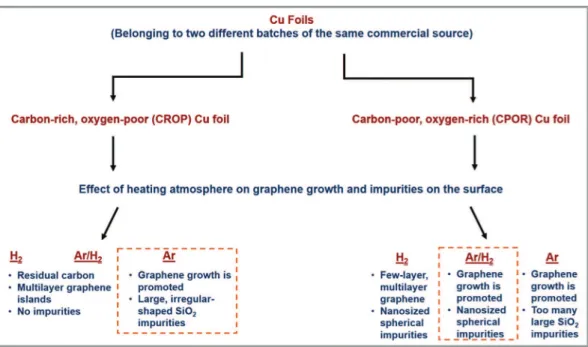
Fig. 11gives a summary of the effect of heating atmosphere on graphene growth during low-pressure CVD method on two different Cu foils (belonging to different batches of the same commercial source) with different surface oxygen and carbon contents. The dashed rectangles indicate the heating atmospheres that provided the highest quality graphene growth on the corre-sponding Cu foils. It should be noted that effective pre-cleaning helped to reduce the amount of impurities on both foils.
Acknowledgements
The financial support for this study by Anadolu University Sci-entific Research Projects Commission (under the project numbers of 1110F155 and 1101F005) is gratefully acknowledged. The authors also thank Jerome Esvan (CIRIMAT, Toulouse) for XPS analyses and Lucien Datas for TEM analyses which were performed at R. Castaing characterization platform, UMS 3623.
Appendix A. Supplementary data
Supplementary data related to this article can be found athttp:// dx.doi.org/10.1016/j.carbon.2016.08.057.
References
[1] C. Lee, X.D. Wei, J.W. Kysar, J. Hone, Measurement of the elastic properties and intrinsic strength of monolayer graphene, Science 321 (2008) 385e388. [2] A.K. Geim, K.S. Novoselov, The rise of graphene, Nat. Mater. 6 (2007) 183e191. [3] A.A. Balandin, S. Ghosh, W.Z. Bao, I. Calizo, D. Teweldebrhan, F. Miao, et al., Superior thermal conductivity of single-layer graphene, Nano Lett. 8 (2008) 902e907.
[4] X.S. Li, W.W. Cai, J.H. An, S. Kim, J. Nah, D.X. Yang, et al., Large-area synthesis of high-quality and uniform graphene films on copper foils, Science 324 (2009) 1312e1314.
[5] Z.Q. Luo, T. Yu, J.Z. Shang, Y.Y. Wang, S. Lim, L. Liu, et al., Large-scale synthesis of bi-layer graphene in strongly coupled stacking order, Adv. Funct. Mater 21 (2011) 911e917.
[6] H.L. Cao, Q.K. Yu, L.A. Jauregui, J. Tian, W. Wu, Z. Liu, et al., Electronic transport in chemical vapor deposited graphene synthesized on Cu: quantum Hall effect and weak localization, Appl. Phys. Lett. 96 (2010) 122106.
[7] S.M. Kim, A. Hsu, Y.H. Lee, M. Dresselhaus, T. Palacios, K.K. Kim, et al., The effect of copper pre-cleaning on graphene synthesis, Nanotechnology 24 (2013) 365602.
[8] L. Gan, Z.T. Luo, Turning off hydrogen to realize seeded growth of sub-centimeter single-crystal graphene grains on copper, Acs Nano 7 (2013) 9480e9488.
[9] H.L. Zhou, W.J. Yu, L.X. Liu, R. Cheng, Y. Chen, X.Q. Huang, et al., Chemical vapour deposition growth of large single crystals of monolayer and bilayer graphene, Nat. Commun. 4 (2013) 2096.
[10] Y.F. Hao, M.S. Bharathi, L. Wang, Y.Y. Liu, H. Chen, S. Nie, et al., The role of surface oxygen in the growth of large single-crystal graphene on copper, Science 342 (2013) 720e723.
[11] D.H. Jung, C. Kang, M. Kim, H. Cheong, H. Lee, J.S. Lee, Effects of hydrogen partial pressure in the annealing process on graphene growth, J. Phys. Chem. C 118 (2014) 3574e3580.
[12] Y.C. Shin, J. Kong, Hydrogen-excluded graphene synthesis via atmospheric pressure chemical vapor deposition, Carbon 59 (2013) 439e447.
[13] D.A. Shirley, High-resolution X-ray photoemission spectrum of the valence bands of gold, Phys. Rev. B 5 (1972) 4709e4714.
[14] J.H. Scofield, Hartree-Slater subshell photoionization cross-sections at 1254 and 1487 eV, J. Electron Spectrosc. Relat. Phenom. 8 (1976) 129e137. [15] X.L. Liang, B.A. Sperling, I. Calizo, G.J. Cheng, C.A. Hacker, Q. Zhang, et al.,
Toward clean and crackless transfer of graphene, Acs Nano 5 (2011) 9144e9153.
[16] S.D. Costa, A. Righi, C. Fantini, Y.F. Hao, C. Magnuson, L. Colombo, et al., Resonant Raman spectroscopy of graphene grown on copper substrates, Solid State Commun. 152 (2012) 1317e1320.
[17] Y. Hernandez, V. Nicolosi, M. Lotya, F.M. Blighe, Z.Y. Sun, S. De, et al., High-yield production of graphene by liquid-phase exfoliation of graphite, Nat. Nanotechnol. 3 (2008) 563e568.
[18] M.S. Dresselhaus, A. Jorio, M. Hofmann, G. Dresselhaus, R. Saito, Perspectives on carbon nanotubes and graphene raman spectroscopy, Nano Lett. 10 (2010) 751e758.
[19] A.C. Ferrari, J.C. Meyer, V. Scardaci, C. Casiraghi, M. Lazzeri, F. Mauri, et al., Raman spectrum of graphene and graphene layers, Phys. Rev. Lett. 97 (2006) 187401.
[20] L.M. Malard, M.A. Pimenta, G. Dresselhaus, M.S. Dresselhaus, Raman spec-troscopy in graphene, Phys. Rep. 473 (2009) 51e87.
[21] C.W. Magnuson, X.H. Kong, H.X. Ji, C. Tan, H.F. Li, R. Piner, et al., Copper oxide as a “self-cleaning” substrate for graphene growth, J. Mater Res. 29 (2014) 403e409.
[22] I. Vlassiouk, P. Fulvio, H. Meyer, N. Lavrik, S. Dai, P. Datskos, et al., Large scale atmospheric pressure chemical vapor deposition of graphene, Carbon 54 (2013) 58e67.
[23] H.J.T. Ellingham, Reproducibility of oxides and sulphides in metallurgical processes, J. Soc. Chem. Ind. 63 (1944) 125e133.
[24] Y.F. Zhu, K. Mimura, Y. Ishikawa, M. Isshiki, Effect of floating zone refining under reduced hydrogen pressure on copper purification, Mater Trans. 43 (2002) 2802e2807.
[25] J.W. Lim, M.S. Kim, N.R. Munirathnam, M.T. Le, M. Uchikoshi, K. Mimura, et al., Effect of Ar/Ar-H2plasma arc melting on Cu purification, Mater Trans. 49
(2008) 1826e1829.
Fig. 11. Summary of the relationship between heating atmosphere and Cu foil impurities during graphene growth via low pressure CVD. (A color version of this figure can be viewed online.)