Pépite | Vers un processus de dépôt entièrement en pulvérisation cathodique pour la fabrication de cellules solaires à base de CIGS : du dépôt des couches minces élémentaires à la caractérisation du dispositif
197
0
0
Texte intégral
(2) Thèse de Boubakeur Ayachi, Lille 1, 2016. © 2016 Tous droits réservés.. II. lilliad.univ-lille.fr.
(3) Thèse de Boubakeur Ayachi, Lille 1, 2016. Acknowledgements. The work of this PhD thesis has been done at the IEMN (Institut d’Electronique, de Microélectronique et de Nanotechnologie), with a financial support from Université de Lille1. First of all, I would like to thank, Dr. Jean-Pierre Vilcot, for having accepted me as a PhD student under his supervision, for his guidance and continuous encouragement and finally for carefully correcting this work. I would also like to thank all members of the Optoelectronic group. Thanks to Thomas for being my tutorial during my first days in the clean room. One advice for him: slow down, slowly but surely and better late than never!! Thanks to Marc, Guillaume, David and the pseudo-Japanese Etienne for their technical help. Special thanks to Mr. Patrick Chapon from HORIBA Jobin-Yvon group for the GDOES analyses, without which our cells would have never transformed the light of the day!!! Without forgetting to thank Dr. Pascal Roussel, Dr. Dominique Vignaud and Dr. David Troadec for the XRD, Raman and FIB analyses, respectively. Finally, I would like to thank the committee members Dr. Denis Mencaraglia, Dr. Frédérique Ducroquet, Dr. Marie-Paule Besland, Dr. Patrice Miska, Dr. Phillipe Torchio, for having accepted to review this work.. Thanks to all of those who have helped and contributed, directly or indirectly, to this work.. © 2016 Tous droits réservés.. III. lilliad.univ-lille.fr.
(4) Thèse de Boubakeur Ayachi, Lille 1, 2016. © 2016 Tous droits réservés.. IV. lilliad.univ-lille.fr.
(5) Thèse de Boubakeur Ayachi, Lille 1, 2016. Contents Introduction ..................................................................................................................................... 1 Chapter 1: Back contact ...........................................................................................................................7 Part A. State of the art 1.1. Why molybdenum (Mo) as a back contact material for CIGS solar cells in standard configuration (substrate configuration with ±2.5µm thick CIGS absorber layer)? ...................9 1.1.1.Metal-semiconductor contact nature ................................................................................9 1.1.2.Effect of sputtering deposition conditions on molybdenum layer properties ............... 10 1.1.3.Multilayer structure ........................................................................................................ 11 1.1.4.Sodium out-diffusion control .......................................................................................... 11 1.2. Alternative back contact materials ........................................................................................ 12 1.2.1.Back contact for reduced CIGS absorber layer thickness ................................................ 12 1.2.2.Transparent back contact for bifacial and tandem cells ................................................. 13 1.3. Substrate bending after annealing.......................................................................................... 13 1.4. Different sources of stress in sputtered thin films ................................................................. 14 1.4.1.Thermal stresses ............................................................................................................. 14 1.4.2.Intrinsic stresses .............................................................................................................. 15 1.4.2.1. Tensile stresses .................................................................................................... 15 1.4.2.2. Compressive stresses .......................................................................................... 15 1.4.3.Extrinsic stresses ............................................................................................................. 16 1.5. Partial conclusion .................................................................................................................... 17 Part B. Experimental results 1.6. Background and problematic .................................................................................................. 18 1.7. Proposed model explaining substrate bending ...................................................................... 18 1.8. Annealing of air stocked molybdenum thin films ................................................................... 21 1.9. Reactively sputtered Mo(O) thin films .................................................................................... 21 1.10. Mo(O)/Mo bilayer structure for a perfect flatness of substrates .......................................... 25 1.11. Chapter conclusion ................................................................................................................ 27 Chapter 2: Absorber layer .................................................................................................................... 29 Part A. State of the art 2.1. CIGS material........................................................................................................................... 31 2.1.1.Structural properties ....................................................................................................... 31 2.1.2.Optoelectronic properties ............................................................................................... 31 2.2. Deposition techniques ............................................................................................................ 32 2.2.1.One stage evaporation process....................................................................................... 32 2.2.2.Two stages evaporation process ..................................................................................... 32 2.2.3.Three stages evaporation process .................................................................................. 33 2.3. Sputtering process ................................................................................................................. 33. © 2016 Tous droits réservés.. V. lilliad.univ-lille.fr.
(6) Thèse de Boubakeur Ayachi, Lille 1, 2016. 2.3.1.Sputtering from multi targets ......................................................................................... 33 2.3.2.Sputtering from ternary target ....................................................................................... 34 2.3.3.Sputtering from quaternary target ................................................................................. 34 2.4. CIGS orientation ..................................................................................................................... 35 2.4.1.Origins of preferential orientation .................................................................................. 35 2.4.2.Effect of preferential orientation on cells performance ................................................. 36 2.5. Impurities effect ..................................................................................................................... 37 2.5.1.Metallic elements effect ................................................................................................. 37 2.5.2.sodium effect .................................................................................................................. 37 2.5.3.Potassium effect .............................................................................................................. 38 2.6. The role of the band gap engineering ..................................................................................... 39 2.6.1.Simple graded band gap.................................................................................................. 39 2.6.2.Double graded band gap ................................................................................................. 39 2.6.3.Double grading profile and its effect .............................................................................. 40 2.7. MoSe2 interfacial layer ............................................................................................................ 40 2.7.1.Formation conditions ...................................................................................................... 40 2.7.2.Effect on CIGS adhesion and metal-semiconductor contact type .................................. 41 2.8. Partial conclusion .................................................................................................................... 41 Part B. Experimental results 2.9. Stack of reduced thickness CIGS bilayers for argon outgassing management ....................... 44 2.10. Third developed process: high pressure process................................................................... 50 2.11. Short annealing time process ‘’10 min‘’ ............................................................................... 54 2.12. Induced cracks in molybdenum after CIGS recrystallization ................................................ 56 2.13. CIGS thin film orientation control .......................................................................................... 58 2.13.1. Effect of molybdenum density .................................................................................... 58 2.13.2. In-situ annealing: Back side heating effect .................................................................. 61 2.14. Chapter conclusion ................................................................................................................ 62 Chapter 3: Buffer layer ......................................................................................................................... 65 Part A. State of the art 3.1. Buffer layer roles ..................................................................................................................... 67 3.2. CBD-CdS buffer layer and its alternatives ............................................................................... 68 3.2.1.CBD-CdS advantages ....................................................................................................... 68 3.2.2.CBD-CdS drawbacks ........................................................................................................ 68 3.2.3.Essential criteria of the optimal alternative buffer layer ................................................ 68 3.2.4.Alternative buffer layers ................................................................................................. 69 3.2.5.Buffer layer free process (P-n buried junction by diffusion) .......................................... 70 3.3. Zinc oxy-sulfide (ZnOS) layer: properties and deposition techniques .................................... 70 3.3.1.Optoelectronic and structural properties ....................................................................... 70 3.3.2. Deposition techniques for CIGS solar cells ..................................................................... 72 3.4. ZnOS buffer layer thickness ................................................................................................... 73 3.4.1.Ultra-thin (≤5nm) ........................................................................................................... 73 3.4.2.Thin (10-30nm) ............................................................................................................... 73. © 2016 Tous droits réservés.. VI. lilliad.univ-lille.fr.
(7) Thèse de Boubakeur Ayachi, Lille 1, 2016. 3.4.3.Medium thickness (50-60nm) ........................................................................................ 74 3.4.4.Relatively thick (≥100nm) ............................................................................................... 74 3.5. Buffer layer annealing ............................................................................................................. 74 3.5.1.CdS layer .......................................................................................................................... 74 3.5.2.ZnOS layer ....................................................................................................................... 75 3.6. Partial conclusion: summary and work to do ......................................................................... 75 Part B. Experimental results 3.7. Chemical bath deposition of CdS layer ................................................................................... 77 3.7.1.Deposition protocol......................................................................................................... 77 3.7.2.Growth and coverage ...................................................................................................... 78 3.7.3.Structural and optical properties .................................................................................... 82 3.8. Sputtered ZnOS layer .............................................................................................................. 84 3.8.1.Reactive sputtering process ............................................................................................ 84 3.8.2.ALD-inspired sputtering process ..................................................................................... 86 3.8.2.1. Deposition protocol ............................................................................................. 86 3.8.2.2. Optical characterization ...................................................................................... 87 3.8.2.3. Structural and morphological characterization ................................................... 90 3.8.2.4. Effect of substrate continuous rotation............................................................... 96 3.8.3.Alternative process: Low sputtering power ZnSxO1-x thin films ...................................... 97 3.9. Chapter conclusion ................................................................................................................. 98 Chapter 4: Window layer.................................................................................................................... 101 Part A. Stat of the art 4.1. The role of the window layer ................................................................................................ 103 4.2. Intrinsic and doped ZnO properties ..................................................................................... 104 4.2.1.Structural ....................................................................................................................... 104 4.2.2.Electrical ....................................................................................................................... 104 4.2.2.1. Origins of n type conductivity in i-ZnO .............................................................. 104 4.2.2.2. Origins of n type conductivity in intentionally doped ZnO ................................ 105 4.2.2.3. Mechanisms limiting electrons transport ......................................................... 105 4.2.3.Optical ........................................................................................................................... 106 4.3. Detailed overview on AZO thin films .................................................................................... 107 4.3.1.Deposition techniques: Why sputtering?...................................................................... 107 4.3.2.Effect of different sputtering parameters ..................................................................... 109 4.3.2.1. Deposition temperature .................................................................................... 109 4.3.2.2. Reactive gas: O2.................................................................................................. 109 4.3.2.3. Doping concentration ........................................................................................ 110 4.3.2.4. Other sputtering parameters ............................................................................ 110 4.3.3.AZO surface engineering/texturing for light trapping................................................... 110 4.4. Partial conclusion .................................................................................................................. 111 Part B. Experimental results 4.5. Effect of deposition pressure and argon flow....................................................................... 112. © 2016 Tous droits réservés.. VII. lilliad.univ-lille.fr.
(8) Thèse de Boubakeur Ayachi, Lille 1, 2016. 4.6. Effect of sputtering power and thin films thickness ............................................................. 116 4.7. Effect of pulse parameters (duty cycle) ............................................................................... 118 4.8. Thickness variation along a diameter of 2" SLG substrate ................................................... 119 4.9. Effect of rapid thermal annealing ........................................................................................ 119 4.10. RF deposited AZO thin films ................................................................................................. 128 4.11. Low temperature RTA .......................................................................................................... 130 4.12. Origins of limited optoelectronic properties of our samples .............................................. 132 4.13. Chapter conclusion ............................................................................................................. 132 Chapter 5: Solar cells characterization............................................................................................... 135 5.1. 5.2. 5.3. 5.4.. Overall view of cell fabrication process ................................................................................ 137 ZnOS based solar cells: first tests ......................................................................................... 137 Solar cells fabrication using high purity molybdenum back contact .................................... 143 Highly crystalline quality CIGS layer based solar cells .......................................................... 145 5.4.1.High-density molybdenum layer based solar cells ........................................................ 145 5.4.2.Higher temperature annealed CIGS layer based solar cells .......................................... 148 5.5. Sodium post annealing process ............................................................................................ 149 5.6. Chapter conclusion ............................................................................................................... 155 Summary and outlook ....................................................................................................................... 157 Publications and communications .................................................................................................... 163 References........................................................................................................................................... 165. © 2016 Tous droits réservés.. VIII. lilliad.univ-lille.fr.
(9) Thèse de Boubakeur Ayachi, Lille 1, 2016. General introduction. © 2016 Tous droits réservés.. lilliad.univ-lille.fr.
(10) Thèse de Boubakeur Ayachi, Lille 1, 2016. General introduction. © 2016 Tous droits réservés.. -2-. lilliad.univ-lille.fr.
(11) Thèse de Boubakeur Ayachi, Lille 1, 2016. General introduction Motivation. At research level, the copper-indium-gallium-selenium (CIGS) thin film technology exhibits a now record efficiency of 22.3% to be compared to bulk silicon technology which is at 25% and 25.6% for monocrystalline and heterojunction with intrinsic thin-layer (HIT) structures, respectively (non-concentrator illumination) (Figure I.1) [NREL 2016]. The CIGS-based technology has so attracted considerable attention since it can provide high efficiency, more than twice a-Si technology, and less environmental concerns than CdTe technology.. Figure I.1: Best research cell chart [NREL 2016]. (It has to be noticed that higher efficiency values for the CIGS based technology have been recently announced by both ZSW (22.6% certificated)[ZSW] and Solar Frontier (22.8% home measurement) [T. Kato. 2016] ).. © 2016 Tous droits réservés.. -3-. lilliad.univ-lille.fr.
(12) Thèse de Boubakeur Ayachi, Lille 1, 2016. General introduction Nevertheless, thin film technology still faces silicon supremacy even if its raw material consumption is roughly 100 times less and hence thwarts the basic idea that was the seed of its study. However scientific and technical aspects are not solely accountable and geopolitical financial aspects have a major impact on the respective development and deployment of these technologies. We will not enter this debate and we just report factual data on the current and forecast technology deployment [GVR 2016]. Main thin film technologies, CIGS and CdTe, contribute equally to share together 8% of the whole market.. Figure I.2: Germany's market share (actual and forecast) of the main photovoltaic technologies [GVR 2016]. Contrary to bulk silicon technology, thin film solar cell technology is a very promising solution, especially when it is applied to the fabrication of photovoltaic glass for building integrated photovoltaics (BIPV) where the use of crystalline silicon-based technology leads to a rather unpleasant aesthetics with checkerboard visual effect [for example, Himinsun 2016] (Figure I.3a). In such applications, some new designs are based on micro-patterned or laser-machined thin film cells leading to adjustable glass transparency (and consequently power generation) by layout [CROSSLUX 2016].. © 2016 Tous droits réservés.. Figure I.3a: Bulk silicon based BIPV. Fig I.3b: Thin film based BIPV. [Himinsun 2016]. [CROSSLUX 2016]. -4-. lilliad.univ-lille.fr.
(13) Thèse de Boubakeur Ayachi, Lille 1, 2016. General introduction As can be seen on Figure I.1, thin film technologies have recent challengers that are gathered together under the emerging PV banner. Particularly, the perovskite cell family exhibits a sharp performance increase those last years. Nevertheless, these latter still suffer from upscaling and lifetime issues that CIGS technology has already proven to comply with. This is reflected by Figure I.2 where no deployment, and so related industrial development, of such technologies are forecast in the following years. One of the key steps in the fabrication of CIGS-based solar cells is the choice of the absorber deposition technique, to which, cells performance is strongly dependent. Furthermore, the choice of the nature and the deposition technique of the buffer layer is another crucial step for achieving high performance solar cells. At the industrial level, several companies working in this field have developed their appropriate process. In table I.1, we present the used process and the achieved efficiency by the two pioneer manufacturers of CIGS thin film photovoltaic solar panels.. Company. Solar Frontier [Solar Frontier]. AVANCIS [AVANCIS]. Back contact. Sputtered molybdenum layer. CIGS deposition process. Two steps process: material sputtering/selenization. Buffer layer: process/nature. CBD/ZnSxO1-x. Window layer Sub-module efficiency % Advantages of using sputtering process for CIGS layer deposition CIGS process Drawbacks Buffer layer nature/process. Evaporation/InxSy. i-ZnO/IIIA-doped ZnO 17.5. 17.9. High deposition rate Good uniformity over large surfaces Low cost High yield The need for a selenization step is still pointed out as a real issue Waste recycling of ZnOS solution. High-cost. Table I.1: Followed process by the pioneer manufacturers of CIGS thin film photovoltaic solar panels: advantages and drawbacks. (It has to be noticed that efficiency values are here different from the ones shown in Figure I.1 that refer to elementary cell data). Thin film cell technology development and in a broader term photovoltaic research activity started at IEMN in 2009 by the PhD of Thomas Aviles in the frame of a "Délégation Générale à l'Armement" support. The goal was to investigate an energy harvesting technology able to be integrated with other electronic functions onto the same chip. Photovoltaic technology was. © 2016 Tous droits réservés.. -5-. lilliad.univ-lille.fr.
(14) Thèse de Boubakeur Ayachi, Lille 1, 2016. General introduction then focused on since it allows furnishing larger energy amount that other alternatives such as piezo- or thermo-electricity at this scale. Co-integration led us to thin film technology and our core trade to physical vapor deposition. At that time, such an approach was quite innovative, moreover taking into account the different guidelines we self-imposed. Main were: i) use of single target for absorbing layer, ii) removal of hazardous gas or process and iii) decrease of thermal budget. This PhD work is so in continuation of the previous PhD work of Thomas Aviles It has been carried out in close collaboration with the new startup ‘’CROSSLUX’’ which works on the development of photovoltaic glass for building integrated photovoltaics (BIPV) (see Figure I.3b) Thomas Aviles is additionally involved in. Our ultimate goal is then developing a full sputtering deposition process. Furthermore, reaching a reduced environmental footprint drove us removing both selenization step and cadmium material from the fabrication process. Scientific approach. The outcome of these 3 years of PhD work is structured in five chapters. Chapters 1 to 4 are composed of two parts: a first part in which the state of the art is given, while in the second part we present our scientific contributions. CIGS cells being studied from a while, we thought it was important to make a clear situational analysis before describing our work. The first chapter will be devoted to understand the role of molybdenum layer as a back contact, to understand, explain and develop an innovative solution for the commonly reported substrate bending issue which can be of real concern in the BIPV application targeted by CROSSLUX (up to 2m x 4m window glass size, in fine). In the second chapter, after a very detailed overview on the already obtained results, an original deposition process for the absorber layer will be presented. It gathers the three main guidelines reported above, i.e. the use of a single quaternary target, no use of Se based process and limited thermal budget. The purpose of the third chapter will be to develop a standard (CBD-CdS) and an alternative (room temperature sputtered zinc oxysulfide (ZnSxO1-x)) buffer layers. Basically, only zinc oxysulfide approach by sputtering was studied. However, the chemical bath deposition technique for a usual CdS layer was developed in order to separate absorbing and buffer layer contribution in cell performance as well as to compare more easily with literature results. Our contribution in the development of a sputtering process for the deposition of the window layer will be the subject of chapter 4. The electrical characterizations and the microstructural analyses of full fabrication stages towards the fabrication of working solar cells will be presented in chapter 5, before ending this manuscript with the conclusions and a brief outlook.. © 2016 Tous droits réservés.. -6-. lilliad.univ-lille.fr.
(15) Thèse de Boubakeur Ayachi, Lille 1, 2016. Chapter 1: Back contact. This chapter is mainly devoted to the development of an innovative solution for the commonly reported substrate bending issue. In the first part, we will justify the choice of both molybdenum material and sputtering deposition technique for the deposition of the CIGS solar cell back contact. We will also give a quick review on alternative materials for specific application, their advantageous and drawbacks. A special interest will be addressed to the commonly reported substrate bending issue. Finally, since we believe that this substrate bending is, in somehow, related to the stress state of the as-deposited thin films, a detailed review on the origin of different stresses within sputtered thin films will be given. In the second part, we will first start by proposing a simple model explaining the dependence of substrate bending on the initial stress state of the molybdenum layer. Then, we will show that it is possible to overcome this issue by simply using a reactive sputtering process for the deposition of the molybdenum layer. Finally, we will show that using a bilayer structure Mo/Mo(O) allows a more precise control of the flatness of the annealed samples.. © 2016 Tous droits réservés.. lilliad.univ-lille.fr.
(16) Thèse de Boubakeur Ayachi, Lille 1, 2016. Chapter 1: Back contact. © 2016 Tous droits réservés.. -8-. lilliad.univ-lille.fr.
(17) Thèse de Boubakeur Ayachi, Lille 1, 2016. Chapter 1: Back contact Part A. State of the art. 1.1. Why molybdenum (Mo) as a back contact material for CIGS solar cells in standard configuration (substrate configuration with ±2.5 µm thick CIGS absorber layer)?. Over more than four decades of chalcopyrite solar cells development, molybdenum is always used as a reference back contact material ‘’thanks to its low cost and abundance, excellent mechanical and electrical properties, low reactivity with and diffusivity into the CIGS layer, ability to conserve this properties at/after high temperature deposition/annealing process of CIGS, and its ability to form an ohmic contact with the CIGS absorber layer’’. On the other hand, sputtering deposition technique is commonly used for the deposition of molybdenum back contact of CIGS solar cells. In addition to the reduction in fabrication cost, the use of sputtering offers the possibility to manage the stresses within the molybdenum layer. Furthermore, sputtered molybdenum layer density, which is easily controlled by changing the deposition conditions, is known to play a very important role in controlling the out-diffusion of alkaline elements from the substrate. All these advantages and others, related to both molybdenum material and sputtering deposition technique, make of the sputtered molybdenum layer a back contact of choice for CIGS solar cells. In the following, we give some details on the most important points previously highlighted. 1.1.1.Metal-semiconductor contact nature. One very important point that should be taken in consideration while choosing the back contact material is the nature of the metal/semiconductor (CIGS absorber) contact: forming a low resistivity ohmic contact is a mandatory condition for a better carrier collection and lower interface recombination. The nature of a metal/p-semiconductor contact is commonly expressed using the Schottky model, which shows the hole barrier height (Φbp) dependence on both the band gap (Egsc) and electronic affinity (χsc) of the p-semiconductor, on one side and on the other side, on the work function of the metal: Φbp= Egsc+χsc – Φm Taking into consideration that an ohmic contact is only achievable for a low hole barrier height (Φbp), and both band gap (Egsc) and electronic affinity (χsc) of the p-semiconductor are constant (for a given CIGS), therefore it is clear that the use of high work function metal (Φm) is mandatory to get an ohmic contact. Theoretical calculations have shown that the barrier height should be less than 0.3 eV, otherwise cell characteristics will be affected. As a consequence, the use of a metal with a work function higher than 5 eV seems to be necessary [A. Simchi. 2014 and references therein] .. © 2016 Tous droits réservés.. -9-. lilliad.univ-lille.fr.
(18) Thèse de Boubakeur Ayachi, Lille 1, 2016. Chapter 1: Back contact Consequently, one can expect that a rectifying contact nature should take place in case of using molybdenum due to its low work function (around 4.4 eV); whereas, this expectation is in contradiction with experimental results in which an ohmic contact characteristics is commonly reported [T. Wada. 2001]. In fact, the use of a Schottky model to explain experimental observations might be confusing, since it does not take in consideration neither the surface chemistry of both sides nor their defect densities, which might highly influence the contact type in real conditions [E.H. Rhoderick. 1970] . Furthermore, this model is only valid for abrupt interfaces which is not the case for molybdenum-high temperature deposited/annealed CIGS interface. A deep investigations of the Mo-CIGS interface have revealed the existence of an interfacial layer (MoSe2), to which the ohmic contact behavior is commonly attributed [T. Wada. 2001] [D. Abou-Ras. 2005] . This MoSe2 layer is, in few words, the result of selenium reaction with molybdenum surface during the high temperature deposition/annealing process (more details will be presented in §2.7). 1.1.2.Effect of sputtering deposition conditions on molybdenum layer properties. It is commonly reported that the kinetic energy of the sputtered Mo atoms arriving at the substrate surface, which is itself dependent of both sputtering power and pressure, is a critical parameter for the resulting layer properties. From the crystallographic point of view, highly oriented (110) sputtered molybdenum layers are commonly achieved on glass substrates independently of the sputtering conditions and even when (100)-textured molybdenum foils are used as substrates [M. A. Contreras. 2000]; however, an enhancement of the crystalline quality is commonly reported for lower sputtering pressures (higher kinetic energy of the sputtered Mo atoms at the substrate surface) [C. Roger. 2013] [Z.H. Li. 2011] . In parallel to that, is was also found that the resistivity of sputtered molybdenum layers depends on the crystalline quality and therefore on the sputtering deposition conditions: the higher the kinetic energy of the sputtered Mo atoms at the substrate surface, the lower the resistivity is [M. Jubault. 2011] [Z.H. Li. 2011] [C. Roger. 2013]. On the other hand, the induced stresses within the sputtered molybdenum layers are also believed to be dependent on the deposition conditions. As the deposition pressure increases, the stress state changes from highly compressive to highly tensile passing by a zero point (stress free point at low pressure) and then again down to zero (stress free point at high pressure) [H.A. Al-Than. 2001]. In fact, this is a characteristic that is related to the sputtering technique rather than the molybdenum material itself [J.A. Thornton. 1977]. A detailed study of the origins of stresses within the sputtered molybdenum layers will be presented later. Another very important property of sputtered molybdenum layers is the one related to their adhesion to substrate. It is largely reported that sputtered molybdenum layers obtained at low deposition pressure show a poor adhesion to substrate even if they are obtained at a deposition pressure corresponding to the stress free point, while those obtained at high deposition. © 2016 Tous droits réservés.. -10-. lilliad.univ-lille.fr.
(19) Thèse de Boubakeur Ayachi, Lille 1, 2016. Chapter 1: Back contact pressure show a very good adhesion to substrate [J.H. Scofield. 1995]. It is interesting to note that the adhesion is commonly evaluated using the so called tape test. To sum up, using sputtered molybdenum layers with a good adhesion and a low resistivity is mandatory for high efficiency CIGS solar cells. However, obtaining a single molybdenum layer with both properties at the same time seems to be difficult, if not impossible, since the first property is achievable at high deposition pressure while the second is achievable at low deposition pressure (opposing conditions). 1.1.3.Multilayer structure. To overcome the adhesion/resistivity issue, Scofield et al. have developed a sputtered molybdenum bilayer back contact which provides a good adhesion to the substrate while maintaining a low resistivity [J.H. Scofield. 1995]. Their bilayer structure is based on the use of a combination of an adhesion bottom layer and a conductive top layer, sputtered at high and low deposition pressure, respectively. It is worth to note that since the publication of their work in 1995, the bilayer structure became a reference structure, used by everyone, for the deposition of sputtered molybdenum back contact of standard CIGS solar cells (substrate configuration). Furthermore, a trilayer structure was also developed in the last few years. This trilayer structure is based on the addition of a high pressure deposited third layer on the classical bilayer, aiming in controlling the CIGS orientation [D.H. Shin. 2012] [J.H. Yoon. 2014] (more informations will be given in § 2.4.1). 1.1.4.Sodium out-diffusion control. One very important advantage of using sputtered molybdenum layer as a back contact for CIGS solar cells is the possibility of using it as a control valve for sodium out-diffusion (as far as a soda lime glass substrate is used) to the CIGS layer. This sodium out-diffusion is known to be easily controlled by the engineering of the molybdenum layer porosity through the changing of the deposition conditions [J.H. Scofield2. 1995] [P. Bommersbach. 2011] [J.H. Yoon. 2012]. Furthermore, a clear relationship between the amount of the out-diffused sodium and the oxygen concentration within the molybdenum layer (from residual oxygen in the deposition chamber) was also found [J.H. Scofield2. 1995] [P. Bommersbach. 2011]: the higher the oxygen concentration the more important the amount of out-diffused sodium. It is believed that molybdenum oxides at the grain boundaries play an important role in facilitating sodium outdiffusion [M. Bodegard. 1999] [A. Rockett. 1999]. On the other hand, for a better control of the diffused sodium concentration into the CIGS layer and/or to find an alternative sodium source in case of using other substrates than the soda lime glass (flexible substrates: polyimide or metallic foils), sodium doped molybdenum layers as a back contact were recently investigated [J.H. Yun. 2007] [P. Blösch. 2014] [M. Lee. 2015].. © 2016 Tous droits réservés.. -11-. lilliad.univ-lille.fr.
(20) Thèse de Boubakeur Ayachi, Lille 1, 2016. Chapter 1: Back contact 1.2. Alternative back contact materials. In parallel to the development of molybdenum back contact layer for CIGS solar cells, alternative materials such as: Au, Ag, Pt, Ni, Al, Cu, W, V, Cr, Mn, Ta and Nb [K. Orgassa. 2003] [R. J. Matson. 1984] [S. Ashour. 1993] as well as some transparent conductive oxides [T. Nakada. 2005] [P.J. Rostan. 2005] , have also attracted some attention. The reason behind the showed interest for alternative back contact materials is mainly due to the development of other CIGS solar cell structures such as reduced CIGS absorber layer thickness cells, bifacial cells and tandem cells, for which the use of the standard molybdenum back contact is not any more suitable because of either its low reflectivity, its low work function or its opacity. 1.2.1.Back contact for reduced CIGS absorber layer thickness. In standard CIGS solar cells, the fact that molybdenum has a very low optical reflection does not create any problem since the entire incident light should be absorbed within the 2 µm thick CIGS layer. However, for reduced CIGS layer thickness cells, only part of the incident photons which energy is larger than the band gap can be absorbed within a single pass through the absorber. In this case the optical reflection on the back contact might highly affect the cell performance and therefore the use of an alternative material with high optical reflection is highly recommended. For this sake, various materials have been investigated and the obtained results have shown that only few of them (Ag, Au, Al, and Cu) have a high optical reflection [Z.J.L. Kao. 2012]. However, the suitability of Ag, Al, and Cu has been questioned in view of their very low work function which does not meet the ohmic contact requirement. On the other hand, even though Au has shown high optical reflection and high work function, its high diffusivity into the CIGS layer is still considered as a real issue. To overcome these drawbacks, one should either use a room temperature deposition process in order to prevent the metal-CIGS inter-diffusion, or add a transparent conductive oxide intermediate layer between the CIGS and the low work function metal to ensure an ohmic contact. In this scope, Z.J.L. Kao et al. have first used a mechanical lift-off technique to peel a CIGS layer, originally grown on molybdenum, from its substrate and transfer it to another substrate using epoxy glue, and then deposited Au metal at room temperature [Z.J.L. Kao. 2012]. This technique allowed them to fabricate reduced CIGS absorber thickness (down to 400nm) solar cells without (almost not) influencing their performance. However, knowing that the main reason behind the development of the reduced CIGS absorber layer thickness technology is lowering the cell fabrication cost, is it worth to use gold as a back contact material? A combination of high reflectivity metal (Ag) and a transparent conductive oxide (TCO) was also used as a back contact for reduced CIGS layer thickness cells [A. Čampa. 2007]. In this case the TCO has a triple role: (i) in addition to its role as a back contact (see the next section), (ii). © 2016 Tous droits réservés.. -12-. lilliad.univ-lille.fr.
(21) Thèse de Boubakeur Ayachi, Lille 1, 2016. Chapter 1: Back contact it is also used in order to allow non absorbed photons to pass through and to be reflected at the metal surface, and (iii) to prevent the metal diffusion into the CIGS layer. 1.2.2.Transparent back contact for bifacial and tandem cells. In the framework of bifacial and tandem cell development, several groups have shown some interest in developing alternative back contacts using different TCOs. First results have shown that the use of TCOs as back contact is only possible for low temperature CIGS layer deposition processes; otherwise, a dramatic degradation of cells performance take place due to the increase in resistivity of the TCO layer [T. Nakada. 2005]. This increase in resistivity is commonly attributed to the formation of an intermediate Ga2O3 resistive layer in case of using ITO or AZO layer, and to the fluorine depletion in case of using FTO layer [T. Nakada. 2005] [M. Terheggen. 2002] . However, adding a thin molybdenum layer on the top of the TCO before the CIGS absorber layer deposition was found to prevent the formation of the Ga2O3 intermediate layer and to transform the rectifying contact to an ohmic contact [T. Nakada. 2004] [P.J. Rostan. 2005]: thanks to the formation of the MoSe2 layer either by a direct selenization of the deposited Mo layer before CIGS deposition [D. Abou-Ras. 2005] or by classical selenization reaction during CIGS deposition [P.J. Rostan. 2005] . Based on this process, comparable efficiencies to those obtained using standard molybdenum back contact were achieved. 1.3. Substrate bending after annealing. High temperature annealing of molybdenum coated soda lime glass substrates is commonly reported leading to substrates bending. Researchers from Saint-Gobain Glass group have investigated this phenomenon and have concluded that the inhomogeneous temperature distribution over the substrate thickness is the main cause of substrate bending [S. Jost. 2015]. According to them, the observed substrate bending (concave) can be explained as follow: the inhomogeneous temperature distribution leads to a different expansion of the coated side and the uncoated side (since the coated side is heated more than the uncoated side), which results in substrate deformation (convex shape). Then, once reaching the substrate softening point, the substrate bending disappears and the substrate gets back its normal shape (flat), thanks to the mechanical relaxation of stresses due to the viscoelasticity of the substrate. During the cooling down, a greater thermal contraction of the hotter side of the substrate would take place which results in a bended substrate with a concave shape. However, we have to introduce a somewhat discordant note into their explanation since it excludes the possibility of getting convex substrates at the end of the cooling down and we observed such a behaviour in some of our experiments. As a solution, they have proposed the use of a both side heating system and the deposition of an ‘’auxiliary‘’ layer on the uncoated side of the substrate in order to ensure a symmetrization of the temperature gradient along the substrate thickness. In other words, this auxiliary layer. © 2016 Tous droits réservés.. -13-. lilliad.univ-lille.fr.
(22) Thèse de Boubakeur Ayachi, Lille 1, 2016. Chapter 1: Back contact is used to counterbalance the stress existing on both sides of the substrate. One important condition that should be taken in consideration while choosing the auxiliary layer is its chemical neutrality otherwise an additional protective layer will be needed [S. Jost. 2015]. Despite the predicted increase in production cost resulting from the use of an additional layer, the suitability of this proposed solution for the development of photovoltaic windows with controlled transparency should be questioned. A more complete explanation of substrate bending was proposed by C. Broussillou, in which both the temperature distribution throughout the substrate thickness and the tensile stress state of the molybdenum layer (native tensile stresses resulting from the deposition technique and created during the heating up due to the different thermal coefficients) were taken in consideration [C. Broussillou. 2011]. Based on these two explanations, we were able to establish a more generalized model for substrate bending shape dependence, in case of a front side halogen lamps-based heating configuration (RTA furnace), on the stress state within the molybdenum layer (free, tensile or compressive). This model will be presented within the experimental results part. But before that, we believe that a deep understanding of the origin of the different types of stress, as a first step, is important to get in order to find a simpler solution than the one proposed by Saint-Gobain Glass group to avoid substrate bending after the annealing process. 1.4. Different sources of stress in sputtered thin films. Visually, all sputtered thin films deposited on a given substrate are subjected to mechanical stresses. Grouped under the generic term "residual stresses", they result from the contribution of three types of stresses: thermal, intrinsic and extrinsic (not necessarily all of them at the same time). The thermal stresses are due to the difference in the thermal expansion coefficients between the thin film and the substrate (some authors consider them as extrinsic stresses). The intrinsic stresses are the component of stress in the thin film caused by the deposition process itself, known to be easily managed through the control of the deposition process parameters. The extrinsic stresses result from the interaction of the thin film with its surrounding atmosphere (environment) after deposition. 1.4.1.Thermal stresses. When a film coated substrate is at a different temperature from the one used during the film deposition, a thermal stress will occur as a result of the difference in the film and substrate thermal expansion coefficients.. © 2016 Tous droits réservés.. -14-. lilliad.univ-lille.fr.
(23) Thèse de Boubakeur Ayachi, Lille 1, 2016. Chapter 1: Back contact The film thicknesses are generally less than 10-4 times the substrate thickness, therefore plastic deformation of the substrate can generally be neglected and the thermal stresses induced in the thin film are given in a one-dimensional approximation [J.A. Thornton. 1989]: σth= Ef (αf-αs)(Ts - Ta) Where Ef is Young's modulus, αf and αs are the average coefficients of thermal expansion for the thin film and substrate, Ts is the substrate temperature used for the film deposition, and Ta is the temperature of the coated substrate under test. Consequently, room temperature deposited thin films are thermal stress free; however, as the temperature increases, tensile or compressive stresses will take place within those. If the thin film has a higher coefficient of thermal expansion (CTE) than the substrate, then it expands more than the substrate does, resulting in compressive stress generation in the thin film while the substrate surface will be put into tensile stress. If the thin film has a lower CTE than the substrate, then it will be put into tensile stress and the substrate surface into compressive stress. 1.4.2.Intrinsic stresses 1.4.2.1. Tensile stresses. Hoffman’s “grain boundary relaxation” model is the most frequently cited to explain the origin of tensile stress within polycrystalline thin films [R.W. Hoffman. 1976]. This model is based on the consideration of the inter-atomic attractive forces between the columnar grains, inducing an elastic deformation “relaxation”. This tensile stress is inversely proportional to the grains “column” size, while it increases linearly as the distance between grains “columns” increases. The validity/credibility of Hoffman’s model was experimentally verified for several materials [J.A. Thornton. 1977], as well as through numerical simulations [M. Andritschky. 1993]. On the other hand, Abermann and his coworkers have shown through several experimental studies that the tensile stresses in thin films are rather related to the crystallite coalescence [R. Abermann. 1985] . To explain these observations, W.D. Nix et al. have established a model which is based on the crystallite coalescence during the initial stages of growth in polycrystalline thin films with island growth morphology. They concluded that as the growing crystallites get in contact each other at their base, the side-walls zipped together until a balance is reached between the energy associated with eliminating surface area, creating a grain boundary and straining the thin film [W.D. Nix. 1999]. It is worth to note that Nix’ model is not useful for the interpretation of the induced tensile stress in sputtered molybdenum thin films after annealing process due to the high melting temperature of molybdenum, however it could be helpful for the explanation of the induced tensile stress in annealed CIGS layers (next chapter). 1.4.2.2. Compressive stresses. Intrinsic compressive stress was also observed in sputtered molybdenum thin films. The origin of this type of stress was, in the best of our knowledge, discussed for the first time by. © 2016 Tous droits réservés.. -15-. lilliad.univ-lille.fr.
(24) Thèse de Boubakeur Ayachi, Lille 1, 2016. Chapter 1: Back contact F.M. d’Heurle in 1970 [F.M. d'Heurle. 1970]. He supposed that the origin of the compressive stresses in sputtered thin films could be attributed to the "shot-peening" action of the deposited atoms arriving at the surface of the film with considerable kinetic energy. According to d’Heurle, it is conceivable that atoms might be inserted into small interstices, which if they remained empty could cause tensile stresses, but instead cause compressive stresses. Based on this explanation, several models quantitatively predicting the stress within the thin films as a function of the sputtered atoms energy were established. H. Windischmann’s model shows a stress dependence on the physical properties of the film ‘’elastic modulus and molar volume’’ and the incident particles energy [H. Windischmann. 1987]. This model is based on the knock-on linear cascade theory proposed by Sigmund [P. Sigmund. 1969] , and which is only valid when the following three hypotheses are verified: (i) particle energy is high enough to penetrate the surface and randomly displace atoms from their equilibrium positions through a series of primary and recoil collisions, producing a volumetric distortion, (ii) deposition temperature is low, and therefore mass transport and defect mobility is sufficiently low to freeze the volumetric distortion in place, and (iii) the relative volumetric distortion is proportional to the fractional number of atoms displaced from equilibrium sites. For more details, please refer to H. Windischmann’s paper [H. Windischmann. 1987]. In fact, this model shows some limitations: (i) it is not valid if the energetic particles are lighter than the growing thin film atoms, (ii) this model does not predict any limitation for stress as the particles energy increases, while experimental results have shown that there exists a limit energy value, above which the compressive stresses do not increase any more (even decrease) [T. Yamaguchi. 1991]. To overcome these limitations, C.A. Davis has proposed a modified model. While it is still based on the knock-on linear cascade theory, it differs from H. Windischmann’s model by taking in consideration the so called thermal spikes effect ‘’local heating induced by implanted atoms‘’, leading to a local modification of the microstructure and therefore a stress relaxation [K.H. Muller. 1986] [C.A. Davis. 1993]. This model offers a logical explanation of the observed limit in compressive stresses by taking in consideration the existence of a balance between implantation and relaxation processes. 1.4.3.Extrinsic stresses. Post deposition incorporation of impurities, such as oxygen, hydrogen, water vapor and carbon monoxide, is also reported as a source of stress in thin films. The mechanisms inducing such a stress are different and depend on the nature of the incorporated impurity: oxidation, lowering the grains surface energy… etc. E.H. Hirsch has found that tensile stresses in magnesium fluoride take place after exposure to water vapor. According to him, they are originated from the electrostatic dipole interactions between the adsorbed water molecules [E.H. Hirsch. 1980]. In contrast to that, R. Abermann et al. have found that the exposure of chromium thin films to H2O or CO environment gives rise to compressive stresses. They attribute that to the lowering. © 2016 Tous droits réservés.. -16-. lilliad.univ-lille.fr.
(25) Thèse de Boubakeur Ayachi, Lille 1, 2016. Chapter 1: Back contact in surface tension of the metal, owing to saturation of free surface valences at the grain boundary surfaces. On the other hand, they have also found that chromium thin films exposure to H2, CH4 and N2 environment does not affect their stress state, while O2 exposure gives rise to slight compressive stresses which for extended exposure time change to tensile stresses [R. Abermann. 1984]. It is worth to note that those observations have been made on evaporated thin films; however, since the induced stresses were not attributed to the deposition technique but rather to the exposure environment and the material nature, on one hand and on the other hand, knowing that sputtered thin films show in general more porous microstructure, one can then expect similar effects or even more pronounced in case of sputtered thin films exposure to similar environments. 1.5. Partial conclusion. In the first part, we have done our best in order to give a short but complete overview on sputtered molybdenum thin films as a back contact for CIGS solar cells. The reasons behind choosing such a back contact material and deposition technique were discussed. Then a particular interest have been addressed to the commonly reported substrate bending issue: the proposed explanations and the found solution have been reviewed. Finally, we have concluded this first part by reviewing on the origins of stresses within sputtered thin films, since they are believed to be the main cause of substrate bending. In the next part, we will mainly show our innovative/original solution for overcoming the substrate bending issue: starting by proposing a model and then presenting the experimental results.. © 2016 Tous droits réservés.. -17-. lilliad.univ-lille.fr.
(26) Thèse de Boubakeur Ayachi, Lille 1, 2016. Chapter 1: Back contact Part B: Experimental results. 1.6. Background and problematic. After the fabrication of a first set of samples, using Scofield’s bilayer structure [J.H. Scofield. 1995] and checking out the adhesion of the deposited thin films to the substrate (scotch test), mainly two issues have been found: wrinkles at the molybdenum/substrate interface and substrate bending once annealed. Wrinkles at the interface were found to be originated from particles bombardment of the glass substrate surface either during argon plasma etching (further cleaning of the substrate before molybdenum deposition) or during the first stage of the molybdenum thin film deposition. Therefore, this issue was simply overcome by both avoiding the use of the plasma etching step and using a low sputtering power for the deposition of the first 20-30nm of the molybdenum thin film (as a protection layer). In a second time, finding a simple solution for substrate bending was our priority. Therefore and as a first step, molybdenum deposition conditions effect, mainly sputtering power and pressure, was intensively investigated (power and pressure were tuned from very low to very high). Unfortunately, all our attempts were in vain and in the best cases reduced bending was achieved. ‘’We should never give up, failure does not mean impossible’’, that is our principle. 1.7. Proposed model explaining substrate bending. In the following, we will try to explain, through the schematic sketches presented in figure 1.1, the possible scenarios that might occur during and after the annealing of different stress state molybdenum thin films in a front side halogen lamp-based annealing configuration (Rapid Thermal Annealing –RTA- equipment). First of all, one should point out that the initial stress state (i) of the sputtered molybdenum thin films can be different from zero (internal or external stresses can be present) (i >0: tensile stress, i <0: compressive stress) (1); The inhomogeneous temperature distribution throughout the substrate thickness, resulted from the use of such an annealing configuration should be taken in consideration (2); Because the molybdenum layer has a lower expansion coefficient than the substrate, the substrate surface is within compressive stress while the stress state within the molybdenum layer is changed by adding the contribution of the thermal component (th) (2); Up to the softening temperature (Tsoftening), the system (substrate and thin film) expansion is, intuitively, expected to be governed by the substrate because that the film thickness is less than 10-4 times the substrate thickness (3);. © 2016 Tous droits réservés.. -18-. lilliad.univ-lille.fr.
(27) Thèse de Boubakeur Ayachi, Lille 1, 2016. Chapter 1: Back contact One consequence of the inhomogeneity in temperature distribution throughout the substrate thickness is the different expansions of the top and the bottom of the substrate (3); At high temperature, this difference in expansion between the top and the bottom of the substrate is expected to induce a substrate deformation (4); Once reaching the softening temperature, the substrate changes its nature from rigid to viscous fluid-like and therefore the implied forces by molybdenum layer become dominant. At this stage, the molybdenum layer releases its stresses (the initial stresses plus the induced stresses during the heating up ‘’thermal stresses‘’), leading to a substrate deformation (bending); The shape of the induced deformation (bending) depends on both the nature and the intensity of the released stresses (5), (7) & (9); In case that the initial stresses within the molybdenum layer are tensile (σ>0), then both initial and induced (thermal) stresses will pull on the substrate resulting in highly bended substrate with a concave-shape (5); Similarly, stress free molybdenum layer should results in concave shape bended substrate. In this case, only the thermal component of stress will act and consequently less pronounced bending is expected (7); The greater thermal contraction of the hotter side of the substrate during the cooling down will results in a more pronounced concave shape (6) (8); On the contrary, molybdenum layer with highly compressive initial stresses (higher than the induced thermal component) is expected to result in a more pronounced convex shape bending after stresses relaxation (9); Depends on the initial compressive stresses intensity and the annealing temperature, flat or less pronounced convex samples are achievable once cooling down (10) (11); As a conclusion, flat substrate after annealing process can be achieved by simply using asdeposited molybdenum thin films in adequate compressive stresses. This conclusion can explain the obtained reduction in substrate bending using high sputtering power at low deposition pressure.. © 2016 Tous droits réservés.. -19-. lilliad.univ-lille.fr.
(28) Thèse de Boubakeur Ayachi, Lille 1, 2016. Chapter 1: Back contact Halogen lamps. σi: initial stresses.. Temperature distribution gradient. σi. T. Total stress changes due to the contribution of the thermal component. σi+ σth. Due to the low molybdenum layer thickness compared to that of the substrate, the system expansion is governed by the substrate.. σth: thermal stresses. T-ΔT (2). (1). (3). σi+ σth. Substrate deformation due to the different expansions between the top and the bottom. Expansion gradient throughout the substrate thickness corresponding to the temperature gradient. Up to T<Tsoftening (4). T≥Tsoftening σi+ σth=0 (relaxation). σi>0. σi=0. σi<<0; lσil>l σthl. Mo layer tends to relax its tensile stress by pulling on the substrate. Substrate shrinking imposed by the thermal component of stress. Compressive stress relaxation leads to more expansion of the substrate surface. (5). (7). (9). lσil>>l σthl. More pronounced concave shape after cooling down due to the greater thermal contraction of the hotter side of the substrate (6). (8). (10). lσil>l σthl. (11). Depends on the initial compressive stress and the annealing temperature, flat or convex samples are achievable after cooling down. Figure 1.1: Schematic sketches representing the possible scenarios-20that might occur during and after the annealing of different stress state molybdenum thin films in a front side halogen lamps-based configuration..
(29) Thèse de Boubakeur Ayachi, Lille 1, 2016. Chapter 1: Back contact 1.8. Annealing of air stocked molybdenum thin films. The annealing of air stocked molybdenum thin films for more than six months (they have been used as sacrifice samples) during the recalibration of the annealing furnace has led to a surprising result. These samples were supposed to have a concave shape once annealed (previously observed on annealed samples from the same fabrication run); however, a convex shape was obtained!!! At that time, we had no idea about the effect of the surrounding atmosphere on the stress state of the thin films, summarized in section 1.4.3. Based on that and as a first reflection, an accelerated aging process (low temperature annealing either under air environment or O2 gas) was investigated: unfortunately, the obtained results were disappointing. Possible explanations: either oxygen was not at the origin of the changed properties of the aged molybdenum layers or the accelerated aging process led to the formation of an oxide layer at the surface preventing the diffusion of oxygen into the grain boundaries. Whatever was the reason, the accelerated aging process did not work. 1.9. Reactively sputtered Mo(O) thin films. Our persistence in finding a solution for the substrate bending issue has conducted us to the investigation of enforced oxygen incorporation into the sputtered molybdenum layer using a reactive process. The obtained results were more than surprising: we were able to change the bending shape simply by tuning the oxygen flux during the sputtering process. The first obtained set of samples is presented in figure 1.2. As can be seen, the concave bending radius was found to increase when an oxygen flux of 0.4sccm is used, while an oxygen flux of 0.5sccm was found to be sufficient to change the bending shape from concave to very slightly convex. Furthermore, a more pronounced convex bending was observed for an oxygen flux of 0.6sccm, while higher oxygen flux led to a reduced convex bending. Unfortunately, the precise control of the oxygen flux in order to achieve a perfect flatness of the substrate was not possible since the minimum tuning step is 0.1 sccm (precision limit of our sputtering equipment). We should never give up!! An alternative solution to overcome this limitation was found and a perfect flatness of the substrate was achieved. But before presenting this solution, we first present some analyses we have performed to understand the origin of the observed bending changes as a function of oxygen flux.. © 2016 Tous droits réservés.. -21-. lilliad.univ-lille.fr.
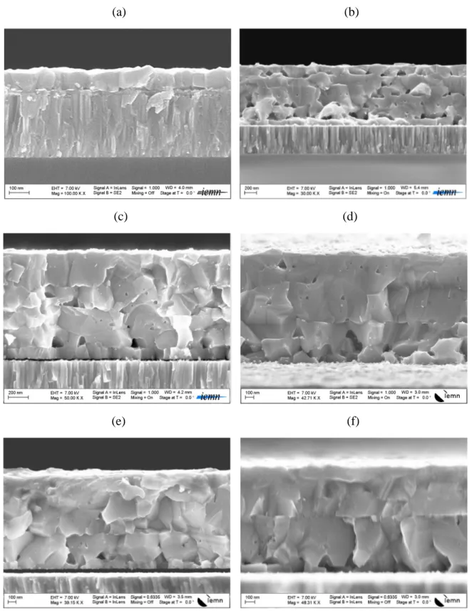
(30) Thèse de Boubakeur Ayachi, Lille 1, 2016. Chapter 1: Back contact 0 sccm. 0.4 sccm. 0.5 sccm. 0.6 sccm. 0.8 sccm. Figure 1.2: Photographs showing the change in bending shape after annealing of reactively sputtered molybdenum thin films on glass substrates as a function of oxygen gas flux. The SEM surface and the corresponding cross sectional images of the reactively sputtered molybdenum thin films using different oxygen flux are presented in figure 1.3. As can be clearly seen, molybdenum thin films microstructure was found to be highly affected by the presence of oxygen during the deposition process. The thin films morphology was found to gradually change from regular grains surface with well-defined edges (for oxygen-free process) to grinded grains surface (for oxygen flux of 0.6sccm). Correspondingly, the cross sectional feature was found to have a gradual change from clear columnar structure to fibrous structure. This change in the microstructure can be simply explained by the knock-on linear cascade theory [P. Sigmund. 1969]: high energy particles penetrate the surface and randomly displace atoms from their equilibrium positions through a series of primary and recoil collisions, producing a volumetric distortion. Consequently, and based on Davies’ model, previously reviewed in section 1.4.2.2, the stress state within the as deposited molybdenum layer is expected to change from tensile to highly compressive. Therefore, applying our model for substrate bending shape dependence on the. © 2016 Tous droits réservés.. -22-. lilliad.univ-lille.fr.
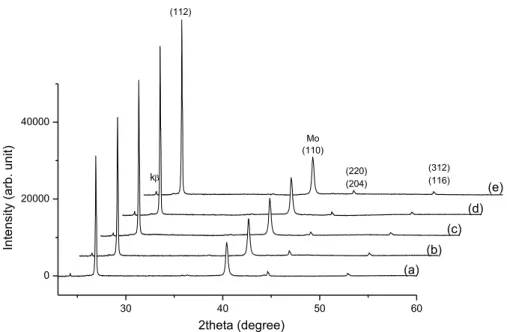
(31) Thèse de Boubakeur Ayachi, Lille 1, 2016. Chapter 1: Back contact initial stress state within the molybdenum layer, one can find out the perfect coherence between the observed change in the bending shape and the found change in microstructure. For higher oxygen flux (0.8sccm), the cross sectional feature and therefore the surface morphology have shown some improvement. This is most likely related to the local heating induced by implanted oxygen atoms (thermal spikes effect), leading to a local modification of the microstructure and therefore balancing, in part, the induced damage. This might explain the reduced compressive stress, and therefore, the increase in bending radius after annealing. On the other hand, XRD analyses, presented in figure 1.4, reveal a decrease in the (110) peak intensity with a shift towards lower diffraction angles as the oxygen flux increase. These observations evidence the crystalline quality deterioration and the change of the stress state, which is in a good consistent with the previous SEM results. Furthermore, no crystalline oxide phases such as MoO2, MoO3 and Mo2O5, were observed; however, that does not mean they are completely absent since they might exist in an amorphous state [T. Yamaguchi. 1991]. Finally, it is of high importance to note that previously reported defects as a consequence of high compressive stresses [J. Tranchant. 2007] were not observed neither before nor after the annealing process.. © 2016 Tous droits réservés.. -23-. lilliad.univ-lille.fr.
(32) Thèse de Boubakeur Ayachi, Lille 1, 2016. Chapter 1: Back contact. Figure 1.3: SEM surface (on the left) and cross sectional (on the right) images of sputtered molybdenum layer at different oxygen flux and annealed at 540oC under N2H2. © 2016 Tous droits réservés.. -24-. lilliad.univ-lille.fr.
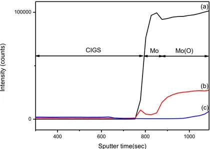
(33) Thèse de Boubakeur Ayachi, Lille 1, 2016. Chapter 1: Back contact. 6000. (110). Mo Mo(O2:0.4sccm) Mo(O2:0.6sccm). Intensity (arb.unit). 4000. 2000. !!. (211). k. (220). 0 30. 60. 90. 2 theta (degree). Figure 1.4: XRD patterns of Mo and reactively sputtered Mo(O) thin films after annealing at 540oC under N2H2. 1.10. Mo(O)/Mo bilayer structure for a perfect flatness of substrates. Because of the faced difficulty in precisely controlling the oxygen flux, an alternative solution was investigated. This is based on counterbalancing the high intensity compressive stress by the deposition of a tensely stressed top layer. Consequently, the total stress of the structure is easily and more precisely controlled by varying the tensely stressed layer to the compressively stressed layer thickness ratio. Furthermore, using this bilayer structure for controlling substrate bending has in fact two additional advantages compared to a single Mo(O) layer: (i) avoiding Ga2O3 formation at the interface with the CIGS layer, (ii) avoiding any series resistance related issues (once integrated in cell fabrication process) due to the observed increase in resistivity of the Mo(O) thin films, as shown in figure 1.5. The elemental distribution throughout the bilayer structure depth was investigated and the obtained SIMS profiles are given in figure 1.6. The SIMS depth profile of oxygen in a single molybdenum layer is also shown as a reference background signal. It is important to note that these analyses have been performed on a complete solar cell structure, and therefore, the elemental profiles are obtained after annealing. As can be seen, the oxygen signal clearly evidences the presence of two layers: Mo and Mo(O). Furthermore, the non-abrupt cut-off in oxygen signal is attributed to the target contamination: the Mo top layer was immediately deposited and no target cleaning was then performed between the Mo(O) and Mo layer deposition steps.. © 2016 Tous droits réservés.. -25-. lilliad.univ-lille.fr.
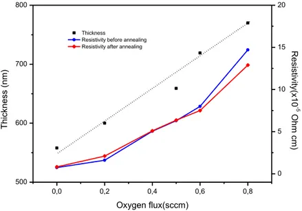
(34) Thèse de Boubakeur Ayachi, Lille 1, 2016. Chapter 1: Back contact On the other hand, the fact that oxygen signal shows a non-zero level within the top molybdenum layer and a slight increase at the interface Mo/CIGS might indicate the oxygen diffusion from the Mo(O) bottom layer to the Mo top layer due to the annealing process. Therefore, a deep investigation of the Mo/CIGS interface seems to be necessary in order to check out whether Ga2O3 is formed or not. If it is the case, adding a buried oxygen-diffusion barrier within the bilayer structure can be used as a solution. Finally, the abrupt change in molybdenum signal at the Mo/Mo(O) interface is believed to be related to the different sputtering rates due to the different matrix structures.. 800. 20. Thickness Resistivity before annealing Resistivity after annealing. 10. -5. Thickness (nm). 700. Resistivity(x10 Ohm cm). 15. 600 5. 0 500 0,0. 0,2. 0,4. 0,6. 0,8. Oxygen flux(sccm). Figure 1.5: Variation of molybdenum thin film thickness and resistivity as a function of oxygen flux.. © 2016 Tous droits réservés.. -26-. lilliad.univ-lille.fr.
(35) Thèse de Boubakeur Ayachi, Lille 1, 2016. Chapter 1: Back contact. (a). Intensity (counts). 100000. CIGS. Mo. Mo(O). (b) (c) 0 400. 600. 800. 1000. Sputter time(sec). Figure 1.6: (a) and (b) SIMS depth profiles of molybdenum and oxygen in a Mo/Mo(O) bilayer structure. (c) SIMS depth profiles of oxygen in a single molybdenum layer. 1.11. Chapter conclusion. Based on previous explanations of substrate bending proposed by S. Jost and J. Palm, and by C. Broussillou, we have proposed a more generalized model showing the dependence of the substrate bending on the initial stress within the molybdenum layer. We have concluded that flat substrates are achievable by simply adjusting the compressive stresses within the molybdenum thin films. Experimentally talking, with some chance and a lot of persistence, an original method for substrate bending management was found. Comparing to that previously patented by S. Jost and J. Palm, our proposed process has the superiority of simplicity and low cost since it does not require the deposition of additional layers on the back surface and it is based on the use of one side heating configuration. The observed change in reactively sputtered molybdenum thin films microstructure and therefore the stress state, on one hand and on the other hand, the corresponding bending shape, were found to be in an excellent coherence with our proposed model for bending dependence on the stress state. For a better control of the initial stress intensity and in order to avoid any undesirable effect on cell performance, Mo/Mo(O) bilayer structure was investigated. The obtained results have shown that it is easier to control the substrate flatness by tuning the top to the bottom layer thickness ratio than by tuning oxygen flux. Finally, using this process for substrate bending management is very useful especially for the development of room temperature deposited CIGS thin films followed by an annealing step. © 2016 Tous droits réservés.. -27-. lilliad.univ-lille.fr.
(36) Thèse de Boubakeur Ayachi, Lille 1, 2016. Chapter 1: Back contact where the recrystallization of the CIGS thin films is found to contribute, in part, into the final substrate bending.. © 2016 Tous droits réservés.. -28-. lilliad.univ-lille.fr.
(37) Thèse de Boubakeur Ayachi, Lille 1, 2016. Chapter 2: Absorber layer. This chapter is devoted to the development of an original deposition process: low cost, easily up scalable and environmentally friendly. We will first start by giving a detailed overview on already obtained results, discussing their advantages and drawbacks. We will also try to find a logical correlation between the obtained results from different laboratories and/or give an interpretation for the divergent points of view and the confusing points. In a second part, we will first start with a quick review on the already obtained results within our group: the solved issues and those still to be resolved. Starting with this, we aim to give a background which justifies our working approaches. Then we will present our contribution and highlight the possible approaches for further improvement.. © 2016 Tous droits réservés.. lilliad.univ-lille.fr.
Figure

+7

Documents relatifs