HAL Id: hal-00492297
https://hal.archives-ouvertes.fr/hal-00492297
Submitted on 28 Jun 2010HAL is a multi-disciplinary open access archive for the deposit and dissemination of sci-entific research documents, whether they are pub-lished or not. The documents may come from teaching and research institutions in France or abroad, or from public or private research centers.
L’archive ouverte pluridisciplinaire HAL, est destinée au dépôt et à la diffusion de documents scientifiques de niveau recherche, publiés ou non, émanant des établissements d’enseignement et de recherche français ou étrangers, des laboratoires publics ou privés.
Anisotropic and inhomogeneous Coulomb screening in
the Thomas-Fermi approximation: Application to
quantum dot-wetting layer system and Auger relaxation
Jacky Even, Charles Cornet, François Doré
To cite this version:
Jacky Even, Charles Cornet, François Doré. Anisotropic and inhomogeneous Coulomb screening in the Thomas-Fermi approximation: Application to quantum dot-wetting layer system and Auger relaxation. physica status solidi (b), Wiley, 2007, 244 (9), pp.3105. �10.1002/pssb.200642334�. �hal-00492297�
A model for anisotropic Coulomb screening : application to
Auger relaxation by 2D and 3D charge carriers in a quantum
dot – wetting layer system
J. Even, C. Cornet and F. Doré
LENS-UMR FOTON 6082 au CNRS, INSA de Rennes, 20 Avenue des Buttes de Coësmes, CS 14315, 35043 Rennes Cedex, France
corresponding author : [email protected] (J. Even)
Abstract.
A model for anisotropic Coulomb screening by 2D and 3D carriers simultaneously, is proposed in the Thomas-Fermi approximation. Analytical expressions for the screened interaction potentials and scattering matrix elements are obtained. This model is applied to the Auger relaxation of carriers in an InAs/InP quantum dot (QD) – wetting layer (WL) system. The influences of the QD morphology and carriers densities on screening and Auger effects are studied. 2D-2D scattering is found to be the most important process, depending especially on QD morphology. A smearing effect is associated to the wetting layer wavefunction extension along the growth axis. The screened potential is similar to a potential screened by 3D carriers.
I. INTRODUCTION
Considerable research developments have been recently achieved in the field of semiconductor quantum dots (QDs). These nanostructures may improve performances of optoelectronic devices as compared to that achieved with semiconductor quantum wells.1-4
Current injection efficiency and modulation dynamics depend crucially on carrier capture and relaxation in the QDs. The importance of Auger processes has attracted much attention from the experimental5-10
and theoretical11-18
points of view. These Auger processes may be associated either to 3D-like carriers or 2D carriers in the wetting layer (WL) (or even QD 0D states) but most theoretical analyses have focused on WL states. The distinction between these two types of carriers is indeed already difficult for quantum well (QW) or QW superlattice19-23
. Bound states in QW (2D carriers) are quite well defined but the situation is much more complicated for continuum states (3D-like carriers). We may also add that the role of WL states in the relaxation processes is still a question debated from the experimental point of view.These various scattering processes are influenced by carrier-induced screening of the electronic interactions24-29
. Some theoretical works11,16,18
use well-known dielectric screening functions for the 2D carriers in the WL in order to simulate the Auger scattering processes involving 2D carriers. The screening for these processes is however associated in another work13
to carriers remaining in the barrier after injection (3D carriers). We believe indeed that the simultaneous roles of 2D WL states and 3D bulk states should be examined within the same model.
In this work, we present briefly a simple one-band model for the calculation of QD electronic discrete states including the WL in a reciprocal space analysis. The detailed simulation of dielectric screening for 2D and 3D electrons is proposed. Auger relaxation processes between the QD first excited and ground states are then described. Results of these
calculations are applied to InAs/InP QDs30-34
. Finally, a discussion is made on the respective roles of 2D and 3D carriers.
II. CALCULATION OF QD AND WL ELECTRONIC STATES
The considered QD is assumed to have a truncated cylinder shape. It is situated on a WL which is more or less similar to a thin QW (figure 1). The simulation of the QD's electronic properties is performed with a simplified one-band effective mass Hamiltonian
( )
r V m H=−h ∆+ conf r 2 2. Owing to the symmetry of the problem (C∞v), the electronic ground
state GS and excited state ES have S and P-like symmetry properties :
( )
( )
ππππ
ϕϕϕϕ
ψ
ψψ
ψ
2 , z r r GS t GS = r (QD 1S state) and( )
( )
ϑϑϑϑππππ
ϕϕϕϕ
ψ
ψψ
ψ
ES t i ES e z r r = ± 2 , r(QD 1P state). The
ϕϕϕϕ
GS( )
rt,z andϕϕϕϕ
ES( )
rt,z functionsare developed in reciprocal space on a basis of products of Bessel and plane waves functions (Bessel-Fourier transform in the radial direction and Fourier transform along the z axis). The
electronic states of the WL
( )
A e z r k t t.r k i w t r r r r Ψ =
, are determined analytically. Only one
discretized energy level is found for Ψw
( )
z in the thin WL studied in this work (figure 1). In the case of InAs/InP QDs, the electronic confinement potential is taken equal to 300 meV in the QD and in the WL, the reduced electronic effective mass to 0.05, the thickness of the WL to 1.2 nm . The description of the WL is similar to the one of a narrow QW. The energy of the unique WL confined electronic stateEw is then equal to –36 meV (the energy isgrowth axis is large, of the order of 10 nm on each side of the WL. The geometry of the InAs/InP QDs (thickness h and radius R) may be controlled during the growth procedure, in particular to tune the optical emission to the telecommunication wavelength (λ=1.55µm)30
. Typical values for thickness and diameter are 2.5nm and 30nm respectively. Electron confinement is then stronger in the growth direction than in the plane. The optical emission energy depends mainly on the thickness h but the energy gap between the ground and excited electronic states EGS −EES is in a first approximation a function of the radius (
meV 19 E
EGS − ES =− for h=2.5nm and R=15nm). We must finally add that several sheets of
QD+WL are often used in order to increase the gain in optical devices. The spacing between QD-WL sheets is generally chosen large enough (L>20nm) to avoid a strong coupling between QD and WL electronic states but not too large to be able to stack several QD-WL sheets in the optical confinement zone. For InAs/InP QDs, typical values for the spacing L are in the 20-40nm range30-34
(figure 1).
III. SCREENING BY 2D AND 3D CHARGE CARRIERS
A. Electronic density of states
We consider the simplified approach of ref. [20] which takes into account the simultaneous presence of 2D carriers localized in a QW and 3D carriers in the barrier. The total electron density is then calculated with :
( )
(
)
∫
( ) ∞ − − + + + = + = 0 / 2 / 3 2 2 / 2 3 2 1 2 1 log dE e E m e L mkT n L n N D D E kT E kT t w µµµµ µµµµππππ
ππππ
h hwhere m is the effective mass, Ew is the quantized level in the WL (only one level is considered),
µ
is the electronic Fermi level and L is the spacing between QD-WL sheets. It is assumed that L is large enough to avoid the appearance of superlattice effects. The energydispersions in the WL and in the bulk are supposed to be parabolic. A single electronic Fermi level is defined for the 2D (n2D) and 3D (n3D) electronic populations. It is possible to define
two carriers temperatures13
but we consider this to be beyond the scope of the present paper. Figure 2-a is a representation of the n2D/(L*Nt)and n3D/Nt variations as a function of Nt
for a spacing L equal to 40nm. The percentages of carriers in the WL and in the barrier remain
stable until N reaches a value of about t
3 17
10 −
= cm
Nt . The filling of 2D electronic states in
the WL is less efficient for larger values of N and t n3D is almost equal to N when t N ist
very large. Figure 2-b shows the variations of n2D and n3D as a function of L for a givenNt
value (Nt =1016cm−3). When L tends to infinity, asymptotic values of n3D and n2D are 2
2
−
= cm
n D 7.45.1010 and n3D =Nt. For very small L values, superlattice effects are
important and this simplified approach is not valid. It corresponds to L<20nm in the InAs/InP QD system32
. For InAs/InP QDs32
, typical values for the spacing L are in the 20-40nm range. We may conclude that in such cases, neither the filling of the WL nor the one of the barrier can be neglected. The simultaneous roles of 2D WL states and 3D barrier states in the screening and in the QD Auger relaxation will then be examined in the following parts
B. Scattering potential screened by 3D carriers
We will follow the classical method of ref [24] extended later to carrier transport in superlattices28
. The scattering potential V
( )
rr induced by a carrier localized at ro ("test"charge) may be obtained by solving Poisson's equation :
( )
r V( )
r V( )
r e[
( )
r n( )
r]
V r =∆ ext r +∆ ind r = − ro + ind r
∆
δ
ε
where
ε
is the dielectric constant of the material, Vext( )
rr
is the unscreened potential, Vind
( )
rr
the induced potential and nind
( )
rr is the induced density of screening carriers. We may notice that such a calculation should provide the same result as a Lindhart-type calculation in the long wavelength limit29. We would like to point out that the expression of V
( )
rr is unchanged by the r ror r
↔ permutation (we will use now the notation V
( )
r ro r r, instead of V
( )
rr ). In the Thomas-Fermi approximation, nind( )
rr is proportional to the potential V( )
r ror r , ,
( )
( )
o D o ind V r r n r r n r,r 3 r,rµµµµ
∂ ∂ −= . The Fourier transform of the Poisson's equation yields
(
)
(
2 2)
2 3 , z z q q e q q V D + =ε
r where q3D = q2 +λλλλ
3−2D and 2 / 1 3 2 3 − ∂ ∂ =µµµµ
εεεε
λλλλ
D D n e . A partial Fourier transform is defined by( )
, 1(
, ,)
iq(rto rt) q o o V q z z e A r r V r r r r r r r −∑
= . The partial Fourier transform of the
"3D-screened" and unscreened potentials are then equal to
(
)
qD z zOD o e q e z z q V = − 3 − 3 2 2 , ,
εεεε
r and(
)
qz zO o ext e q e z z q V = − −εεεε
2 , , 2 rrespectively. We define the dimensionless potentials V
(
q,z,zo)
~ r by
(
o)
V(
q z zo)
q e z z q V ~ , , 2 , , 2 r rεεεε
= . The "3D-screened" dimensionless potential is compared to other
ones on figure 3 for a fixed value of
λλλλ
3D. The curves a) and b) represent the unscreened andthe potential is screened more efficiently when the contribution of 2D carriers is taken into account.
C. Scattering potential screened by 2D carriers with a delta distribution along the z axis
If screening carriers are in bound states of a WL (or QW) and if the wavefunction distribution
along the z axis is replaced by a
δ
function28,
( )
(
t w o) (
w)
D o ind V r z r z z n r r n − ∂ ∂ − =δδδδ
µµµµ
r r r r , , , 2 wherert is the in-plane component of r and zw the position of the WL along the z axis. The Poisson's
equation transforms to
(
)
(
)
(
) (
)
w o w D o ind o ind V q z z z z n e z z q V z z z q V q − ∂ ∂ = ∂ ∂ + −δδδδ
µµµµ
εεεε
, , , , , , 2 2 2 2 2 r r r yielding(
)
(
w o)
z z q D o ind e V q z z n q e z z q V w , , 2 , , 2 2 r r − − ∂ ∂ − =µµµµ
εεεε
. This equation is first applied in the WLplane (z=zw) to find
(
)
µµµµ
εεεε
εεεε
∂ ∂ + = − − D z z q o w n q e e q e z z q V O w 2 2 2 2 1 2 , , r. The classical result28
(
)
(
1)
2 2 2 , − + = D w q e z q Vλ
ε
r with 1 2 2 2 2 − ∂ ∂ =µµµµ
εεεε
λλλλ
D D n efor a pure 2D system is then recovered when the "test " charge is
located inside the WL (zo=zw). The "2D-screened" potential is calculated in a second step at a general position by combining the expressions for V
(
qr,z,z)
, V(
q,z,z)
r
(
)
(
)
(
)
+ − = + = − − − − − − D z z q z z q z z q o ind o ext o q e e e q e z z q V z z q V z z q V O w O w 2 2 1 1 2 , , , , , ,λλλλ
εεεε
r r rThe interaction potential V
( )
rr does not depend anymore on the sole distance between the two charge r ror r
− like in the 3D case. The interaction along the z axis is indeed perturbed by the WL at zw. However the two interacting charges still play the same role, the expression of the potential being unchanged by the z↔ zo permutation. The "2D-screened" (curve c) and
unscreened dimensionless potentials (curve a) are compared in figure 3 for fixed values of
D 2
λλλλ
, q and zo. The anisotropy induced by the 2D carriers is clearly observed. The WL is located at the center of the figure (zw=0). The small value of zo is chosen in order to study the influence of the WL close to it. This might be the case of a charge located inside the QD.D. Scattering potential screened by 3D carriers and 2D carriers with a delta distribution along the z axis
If both contributions are now combined following the two steps method used for the 2D case in part C, the partial Fourier transform of the "2D-3D-screened" potential is :
(
)
(
)
(
)
+ − = + = − − − − − − D D z z q z z q z z q D o ind o ext o q e e e q e z z q V z z q V z z q V D O D w O D w 2 3 3 2 1 1 2 , , , , , , 3 3 3λλλλ
εεεε
r r rWe may remark that when the charges are on the opposite parts of the WL (zw<z<zo or
zo<z<zw), the interaction potential only depends on z−zo . Figure 3-d is a representation of
this potential. The presence of 2D carriers is reflected by a bent at zw=0 into the potential curve like in the "2D-screened" case. The amplitude is further reduced by the 3D carriers. Figure 4 represents the "2D-3D-screened" potential for various positions of the "test" charge along the z axis (zo). The "3D-screened" case is recovered when the "test" charge is located
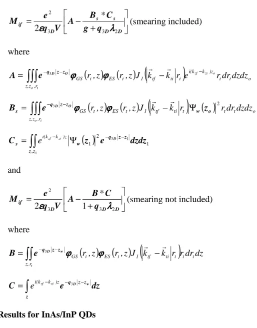
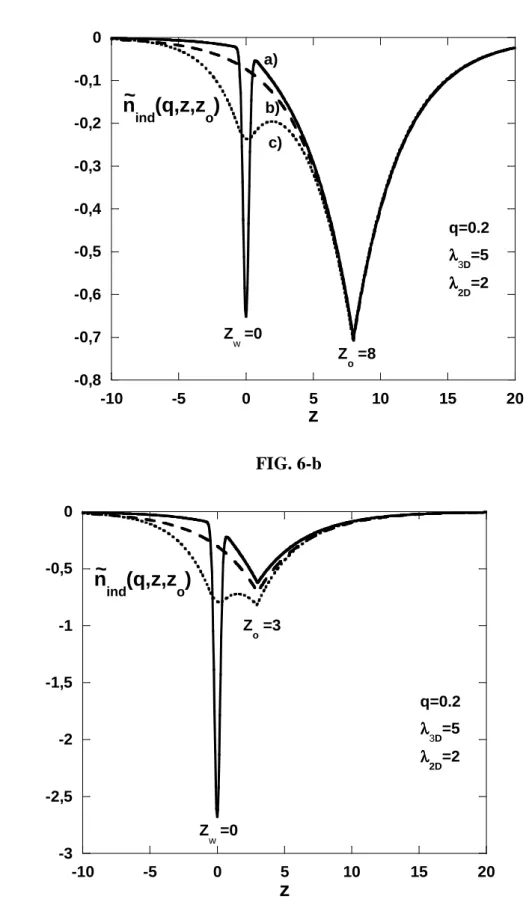
far from the position of the WL. In other words, the influence of 2D carriers on screening is strong only when the "test" charge is located close to the WL. This is indeed the case for a charge located into the QD. Finally, we may point that the strongest screening effect is observed for zo=zw. The "2D-3D-screened" potential has a symmetrical profile only in that case.
E. Screening potential screened by 3D carriers and 2D carriers with WL wavefunction distribution included
The influence of the 2D WL wavefunction distribution along the z axis is now taken into account in the induced density24, 28, 29
:
( )
( )
( ) (
)
( )
o D o t w w D o ind V r r n dz r z r V z z n r r n r,r r, ,r 3 r,r 1 1 2 1 2 2µµµµ
µµµµ
∂ ∂ − Ψ Ψ ∂ ∂ − =∫
where Ψw
( )
z is the z-part of the WL wavefunction for the quantized state. The problem is now more complicate :(
)
(
)
( ) (
)
(
o)
D o w D o ind o ind V q z z n e z q V z n e z z q V z z z q V q , , , , , 3 , , 2 2 2 2 2 2 2 r r r rµµµµ
εεεε
µµµµ
εεεε
∂ ∂ + Ψ ∂ ∂ = ∂ ∂ + −where the potential averaged over the WL wavefunction extension
(
q z)
( ) (
z V q z z)
dzV r, o =
∫
Ψw 2 r, , o appears in the second member. The problem could be solvedself-consistently by putting the solution found in part B in V
(
q,zo)
rat the first step of the computation. It is simpler to extend the method proposed for pure 2D systems 24,25,28,29
.
(
q zo)
V r, is calculated in a first step by integrating the Poisson's equation over z and setting
(
o)
ind q z z V r, , equal to V(
q,z,zo)
Vext(
q,z,zo)
r r − :(
)
− −∫∫
Ψ( )
Ψ( ) (
)
− − ∂ ∂ − = 1 2 2 3 3 , 1 2 1 2 1 2 2 2 3 2 3 2 , , 2 2 , , z z z z q o w w D D z z q D o z z V q z z e dz dz n q e e q e z z q V r D o r Dµµµµ
εεεε
εεεε
then the equation is averaged over Ψw
( )
z 2in a second step to yield :(
)
(
( )
)
+ = D D D o D D o q q g z q f q e z q V 2 3 3 3 3 2 1 , 2 ,λλλλ
εεεε
r where( )
∫∫
( )
( )
− − Ψ Ψ = 1 1 3 , 1 2 1 2 3 z z z z q w w D z z e dzdz q g D and f(
q z)
( )
z e qD z zOdz w o D − −∫
Ψ = 2 3 3 ,It is now possible to integrate numerically the equation over z for any value of zo :
(
)
(
)
( )
( )
( )
2 3 3 2 3 1 2 1 2 2 3 2 2 2 3 3 1 3 , , ~ , , ~ D z z q D D D z z q w w D o ind o ind D O D O D e q g q dz e z z q q z z q V z z z q V qλλλλ
λλλλ
− − − − + + Ψ Ψ = ∂ ∂ + − r r∫
When the WL wavefunction distribution is simplified, the solution to this equation is known
(part B) :
(
)
+ − = − − − − D D z z q z z q D o ind q e e q q z z q V D w O D w 2 3 3 1 1 , , ~ 3 3λλλλ
r .The solutions obtained for the "2D-3D-screened" V
(
q,z,zo)
~ r
taking into account or not the WL wavefunction extension are compared on figure 5 to the "3D-screened" potential:
(
)
D qDz zO o e q q z z q V = 3 − 3 − , , ~ r. The smearing effect associated to the WL wavefunction makes the
"2D-3D-screened" potential with the WL wavefunction included similar to the "3D-screened" potential. In addition the screening induced by the 2D carriers is reduced : the g
( )
q3D factoris smaller than 1. Figure 6 is a representation of the dimensionless induced charge density
(
o)
ind q z z
n~ r, , in the same three cases for two zo values. nind
(
q,z,zo)
~ r
( )
(
)
( ) , , 1 , iq rto rt q o ind o ind n q z z e A r r n r r r r r r r −∑
= and nind
(
qr,z,zo)
=~nind(
qr,z,zo)
q. We have chosen to take a narrow Gaussian-like function to reproduce the delta function (see part B) for the "2D-3D " induced density when the WL wavefunction is not included. The singularity in the induced density is removed by the smearing effect associated to the large spatial extension of the WL wavefunction. In that case the repartition of the induced charge is not very different from the one in a pure 3D case.IV. CARRIER RELAXATION BY AUGER PROCESSES A. Model
Figure 7 is a schematic representation of the four possible Auger scattering processes associated to the relaxation of an electron from the ES to the GS. In the 2D-2D scattering process, the mobile electron remains confined in the WL along the z direction. In the 3D-3D scattering process, the bulk electron remains in the barrier. The two other processes have not been considered previously in the literature. In the 2D-3D scattering process, the mobile electron is emitted from the WL to the barrier whereas the reverse capture from the barrier to the WL is involved into the 3D-2D scattering process.
The relaxation of an electron from the ES to the GS associated to the scattering of 2D or 3D electrons, is determined by the Fermi golden rule :
( )
(
)
∫∫
− = ti tf,k k tf ti ti 2 tf 2 2D -2D d k d k k k 2 R r r r r r r h Mif P Ef Ei Aδδδδ
ππππ
ππππ
, 4 2 2 2 (2D-2D scattering)( )
(
)
∫∫
− = ti f,k k f ti ti 2 f 3 3D -2D d k d k k k 2 R r r r r r r h Mif P Ef Ei V Aδδδδ
ππππ
ππππ
ππππ
, 8 4 2 3 2 (2D-3D scattering)( )
(
)
∫∫
− = i tf,k k tf i i 3 tf 2 3D -2D d k d k k k 2 R r r r r r r h Mif P Ef Ei V Aδδδδ
ππππ
ππππ
ππππ
, 8 4 2 3 2 (3D-2D scattering)( )
(
)
∫∫
− = i f,k k f i i 3 f 3 3D -3D d k d k k k 2 R r r r r r r h Mif P Ef Ei Vδδδδ
ππππ
ππππ
, 8 2 2 3 (3D-3D scattering)where P contains the population factors and Mif is the scattering matrix element
between initial ki
r
and final kf
r
electronic states. In the 2D-3D case, a limitation on the initial wavevector is due to the energy conservation :
(
EGS EES Ew)
m − − ≥ 2 2 h ti k if EGS −EES −Ew ≥0 (2D-3D scattering)B. Direct calculations of scattering rates with WL wavefunction distribution included
As shown in part III-C, the screened potential V
(
q,z,zo)
~ r
can be calculated by a simple 1D numerical integration over the z axis. This computational step is however not necessary for scattering rates matrix elements derived from the application of the Fermi golden rule. For example in the case of the interaction between an electron located in a QW and a Coulombic
impurity at ro29, the scattering matrix element M is equal to if Mif kti rV
( )
r ro ktf r r r r r r r , , , = where( )
A e z r k t t.r k i w t r r r r Ψ =, . Using the results of part III-C, it is straightforward to show that
(
)
iqrto o i f if V k k z e A M r r r r . , 1 −= . This matrix element can thereafter be averaged over the impurity
distribution and the population of 2D carriers.
The electronic relaxation from the QD excited state ES to the QD ground state GS by an Auger process involving the scattering of a 2D carrier (2D-2D scattering) is an extension of this result where the charged QD plays the role of the Coulombic impurity. It depends on the
matrix element Mif kti r ES
( ) ( )
ro V r ro ktf r GS( )
ro r r r r r r r rψ
ψψ
ψ
ψ
ψψ
ψ
, , ; ; ,= (the exchange interaction is
neglected). By introducing the partial Fourier transform of the potential :
(
)
( ) ( )
(
)
∫∫
− − = t r , z, t ti tf 1 t ES t ti tf t t if rdrdzV k k ,z r,z r,z J k k r A 1 M r r r rϕϕϕϕ
ϕϕϕϕ
* GS (2D-2D scattering)The matrix elements for Auger processes involving any type of scattering are calculated in a general way :
(
) (
)
∫∫
− − − = t o o zi zf r , z )z k i(k t ti tf 1 ti tf o t t if rdrdz k k J k k r e V 1 M r r r r o t GS ES r z V , , , (3D-3D scattering)(
) (
)
( )
∫∫
− − Ψ = t o o zf r , z z ik * t ti tf 1 ti tf o t t if rdrdz k k J k k r e L A 1 M VESGS rt zo w zo r r r r , , , (2D-3D scattering)(
) (
)
( )
∫∫
− − Ψ = t o o zi r , z z -ik t ti tf 1 ti tf o t t if rdrdz k k J k k r e L A 1 M VESGS rt zo w zo r r r r , , , (3D-2D scattering)(
) (
)
( )
∫∫
− − Ψ = t o,r z t ti tf 1 ti tf o t t if rdrdz k k J k k r A 1 M VES,GS ,rt,zo w zo 2 r r r r (2D-2D scattering)where VES,GS
(
qr,rt,zo)
=∫
V(
qr,z,zo) ( ) ( )
ϕϕϕϕ
GS rt,zϕϕϕϕ
ES rt,zdz is the average of the potential over the productϕ
GS( ) ( )
rt,zϕ
ES rt,z . In the last case (2D-2D scattering), this formulation is equivalent to the first one given above. The average integral VES,GS(
q,rt,zo)
r
can be expressed using the quantities defined in part III-C :
(
)
(
)
(
)
(
)
∂ ∂ − = o ESGS D t D o t D GS ES D o t GS ES V q z g q r n z r q f q e z r q V , , , , 2 , , 2 , 3 3 , 3 2 , r rµµµµ
εεεε
where(
)
∫∫
( ) ( ) ( )
− − Ψ = 1 1 3 , 1 2 1 3 , , z z z z q w t D GS ES q r z e dzdz g D z , r z , rt ES t GSϕϕϕϕ
ϕϕϕϕ
and f(
q r z)
( ) ( )
e qD z zO dz o t D GS ES − −∫
= 3 , , 3 ,ϕϕϕϕ
GS rt,zϕϕϕϕ
ES rt,zIt is now possible to study the smearing effect of the wavefunction distribution, for example in the case of 3D-3D scattering :
+ − = D D s s D if q g C B A V q e M 2 3 3 2 * 2
εεεε
λλλλ
(smearing included) where( ) ( )
(
)
∫∫∫
− − − − = t o o zi zf r , z z, o t t )z k i(k t ti tf 1 t ES t GS r,z r ,z J k k r e rdrdzdz r rϕϕϕϕ
ϕϕϕϕ
O D z z q e A 3( ) ( )
(
)
( )
∫∫∫
− Ψ = − − t o,r z z, o t t t ti tf 1 t ES t GS r,z r ,z J k k r rdrdzdz 2 3 o w z z q s e z B D O r rϕϕϕϕ
ϕϕϕϕ
( )
∫∫
− Ψ − − = 1 1 3 , 1 2 1 z z z z q w s z e dzdz C i(kzf kzi)z D e and + − = D D D if q C B A V q e M 2 3 3 2 1 *2
εεεε
λλλλ
(smearing not included)where
( ) ( )
(
)
∫∫
− = − − t r z, t t t ti tf 1 t ES t GS r ,z r ,z J k k r rdrdz r rϕϕϕϕ
ϕϕϕϕ
w Dz z q e B 3∫
− − − = z z z q dz e C i(kzf kzi)z 3D w eC. Results for InAs/InP QDs
Figure 8 is a comparison of the QD ES-GS relaxation times for the four Auger processes as a function of the total electron density. The 2D-2D scattering process is the fastest one except for very high densities where the number of accessible final wavevector states for the scattered electrons is reduced by filling effects. The 2D-3D WL to barrier emission is also efficient for assisting the intradot relaxation. Finally the 3D-2D capture of an electron from the barrier to the WL can be neglected.
Figure 9 is a representation of the ratio
ρ
between the 2D-2D (or 3D-3D) relaxation times calculated with and without the effect of the WL wavefunction included. The smearing effect is more important for the 2D-2D relaxation times but the correction to the relaxation time remains small (about 15% at high electron densities).Figure 10-a shows the variation of the relaxation times as a function of the QD radius. In the 2D-2D, 3D-3D and 3D-2D cases, the increase of the radius decreases the relaxation time. This is associated to a change of the QD ES and GS wavefunctions and thus to a change in the scattering matrix elements. In the 2D-3D case, the opposite variation is observed. For large radius, the energy shift EES −EGS is small (figure 10-b). The difference EGS-EW is larger than
EES and as a consequence EGS −EES −Ew ≥0. The number of 2D electronic states available
for emission from the WL to the barrier is limited by the condition
(
EGS EES Ew)
m − − ≥ 22 h ti k .The energy difference EES −EGS increases as the radius decreases down to the value
of R=10nm where EGS −EES =Ew. Below R=10nm, all the WL 2D states are available for
emission of an electron to the 3D states of the barrier. Below R=9nm, only one QD electronic state is quantized and the ES-GS electronic relaxation is not defined. Between R=9nm and R=10nm, the 2D-3D process is slightly more efficient than the 2D-2D process because the number of accessible final wavevector states (3D states instead of 2D states) for the scattered electrons is larger.
The thickness h of the QD may be controlled during the growth procedure30
. Figure 11 shows the variation of the relaxation times as a function of the thickness. The behaviour of the relaxation times versus the thickness is opposite to the one versus the radius (figure 10)
mainly because the energy shift EES −EGS increases when the thickness increases. For QD thicknesses smaller than h=2nm, only one quantized electronic state exists in the QD. In most practical cases, the InAs/InP QD thickness is controlled during the growth procedure in order to tune the emission wavelength of the QD. The distribution of Auger relaxation times should not be very large. Growth studies are performed with the aim to reduce the QD size (mainly the radius) in order to increase the GS-ES energy separation (quantum effect). A small increase of the thickness must be used also in order to keep the emission wavelength at the same value (1.55 µm for example). From the calculated variations of 2D-2D Auger relaxation times as a function of R (figure 10-a) and h (figure 11), we may conclude that both parameters contribute to the slowing down of this 2D-2D induced carrier relaxation. Our study shows however that this slowing down is partly compensated by the speeding up of the 2D-3D carrier relaxation.
V. CONCLUSION
The roles of 2D and 3D electronic states in the screening of a Coulombic interaction are studied. It is shown that 2D and 3D carriers must be taken into account simultaneously, especially when a "test" charge is located near the QW. This is indeed the case for a carrier in a QD and close to a WL. Analytical expressions of the screened potentials are obtained in most cases except in the case where the extension of the 2D bound states along z is taken into account. It is shown however that a simple 1D numerical integration is possible. For the calculation of scattering matrix elements, this numerical step is not necessary and analytical expressions for integrals involving the screened potential are given in all the cases. Intradot carrier Auger relaxation assisted by 2D WL and 3D bulk barrier carriers is studied. New scattering processes involving emission (2D-3D) or capture (3D-2D) of carriers from the WL
to the barrier are analyzed. It is shown however that in most cases the 2D-2D scattering is the predominant process. Changes in the QD morphology not only affect the QD optical emission energy but also the Auger relaxation rates. The 2D-3D process is on the same order of magnitude as the 2D-2D process for a small QD radius.
References 1
M. Grundmann, D. Bimberg and N.N. Ledentsov, Quantum Dot Heterostructures (Chichester: Wiley, 1998).
2
L. Banyai and S.W. Koch, Semiconductor Quantum Dots, World Scientific Series on
Atomic, Molecular and Optical Physics (Singapore, New Jersey, London, Hong-Kong, World
Scientific, 1993), Vol. 2.
3
M. Sugawara, Self-Assembled InGaAs/GaAs Quantum Dots, Semiconductors and
Semimetals (Toronto: Academic, 1999), Vol. 60.
4
Zh. I. Alferov, Quantum Wires and Dots show the Way Forward (III-Vs Rev., 1998), Vol.11, p. 47.
5
B. Ohnesorge, M. Albrecht, J. Oshinowo, A. Forchel and Y. Arakawa, Phys. Rev. B54, 11532 (1996)
6
Z.L. Yuan, E.R.A.D. Foo, J.F. Ryan, D.J. Mowbray, M.S. Skolnick and M. Hopkinson, Physica B 272 12 (1999)
7 S. Sanguinetti, K. Watanabe, T. Tateno, M. Wakaki, N. Koguchi, T. Kuroda, F. Minami and
M. Gurioli, Appl. Phys. Lett. 81 613 (2002)
8
J.I. Lee, I.K. Han, N. Koguchi, T. Kuroda and F. Minami, J. Kor. Phys. Soc. 43 553 (2003)
9
K. W. Sun, J. W. Chen, B.C. Lee and A.M. Kechiantz, Nanotechnology 16 1530 (2005)
10
E.W. Bogaart, J.E.M. Haverkort, T. Mano, T. Van Lippen, R. Nötzel and J.H. Wolter, Phys. Rev. B72 195301 (2005)
11
U. Bockelmann and T. Egeler, Phys. Rev. B46, 15574 (1992)
12
M. Brasken, M. Lindberg and J. Tulkki, Phys. Stat. Sol. (a) 164, 427 (1997)
13
A.Uskov, F. Adler, H. Schweizer and Pilkhun, J. Appl. Phys. 81, 7895 (1997)
14
R. Ferreira and G. Bastard, Appl. Phys. Lett. 74, 2818 (1999)
16
T.R. Nielsen, P. Gartner and F. Jahnke, Phys. Rev. B69, 235314 (2004)
17
R. Wetzler, A. Wacker and E. Schöll, J. Appl. Phys. 95, 7966 (2004)
18
H.H. Nilsson, J. Z. Zhang and I. Galbraith, Phys. Rev. B72, 205331 (2005)
19
G. Bastard, Phys. Rev. Rapid Comm. B30, 3547 (1984)
20 H. Hideki, Y. Miyake and M. Asada, IEEE J. Quantum Electron. 28 68 (1992)
21
G.C. Crow and R.A. Abram, Semicond. Sci. Technol. 10 1221 (1995)
22
G.A. Baraff, Phys. Rev. B55 10745 (1997)
23
B.P.C. Tsou and D.L. Pulfrey, IEEE J. Quantum Electron. 34 318 (1998)
24
F. Stern and W. E. Howard, Phys. Rev. 163, 816 (1967)
25 S. Mori and T. Ando, Phys. Rev. 19 6433 (1979)
26
J.A. Brum, G. Bastard and C. Guillemot, Phys. Rev. B30 905 (1984)
27
J. P. Loehr and J. Singh, Phys. Rev. B42 7154 (1990)
28
J. R. Meyer, D.J. Arnold, C.A. Hoffman and F.J. Bartoli, Phys. Rev. B45 1295 (1992)
29
G. Bastard, Wave Mechanics Applied to Semiconductor Heterostructures (Paris: EDP, 1992)
30
P. Miska, C. Paranthoen, J. Even, N. Bertru, A. Le Corre and O. Dehaese, J. Phys.: Condens. Matter 14, 12301 (2002)
31
C. Cornet, C. Labbé, H. Folliot, N. Bertru, O. Dehaese, J. Even, A. Le Corre, C. Paranthoen, C. Platz and S. Loualiche, Appl. Phys. Lett. 85, 5685 (2004)
32 P. Miska, J. Even, C. Paranthoen, O. Dehaese, A. Jibeli, M. Senes and X. Marie, Appl.
Phys. Lett. 86, 111905 (2005)
33
C. Cornet, C. Platz, P. Caroff, J. Even, C. Labbé, H. Folliot, A. Le Corre and S. Loualiche, Phys. Rev. B 72, 035342 (2005).
34
C. Cornet, C. Levallois, P. Caroff, H. Folliot, C. Labbé, J. Even, A. Le Corre, S. Loualiche, M. Hayne and V. V. Moschalkov, Appl. Phys. Lett. 87, 233111 (2005)
Figure captions
Figure 1 : Schematic representation of the QD-WL system. h and R are the thickness and
radius of the QD respectively. L is the spacing between QD-WL sheets.
Figure 2 : a) Variations of n2D/(L*Nt) (straight line) and n3D/Nt (dashed line) as a
function of N (L=40nm). t n2D/(L*Nt)and n3D/Nt are calculated using the model of part
III-A and represent the percentages of carriers in the WL and in the barrier respectively. b) Variations of n2D (straight line) and n3D (dashed line) variations as a function of
the period L for N =10t 16cm-3. For L<20nm superlattice effects along the z axis can not be
neglected. Asymptotic values of n2D and n3D when L tends to infinity are 1016cm-3 and 7.45
1010
cm-3
respectively.
Figure 3 : Representation of the dimensionless potentials V
(
q,z,zo)
~ r
when the test charge is located at zo=1.5 nm and the WL at zw=0 nm in various cases : a) unscreened potential
(straight line), b) 3D screened potential (dotted line), c) 2D screened potential with the WL wavefunction approximated by a delta z function (dashed line) and d) 2D-3D screened potential corresponding to the b) and c) contributions taken into account simultaneously (dashed and dotted line).
Figure 4 : Representation of the dimensionless 2D-3D screened potential V
(
q,z,zo)
~ r
for various zo values when the WL wavefunction is approximated by a delta function along the
axis.
Figure 5 : Representation of the dimensionless potentials V
(
q,z,zo)
~ r
when the test charge is located at zo=2 nm and the WL at zw=0 nm in various cases : a) unscreened potential (straight
numerical integration (dashed line) and d) 2D-3D screened potential with the WL wavefunction approximated by a delta function (dashed and dotted line).
Figure 6 : Representation of the dimensionless induced charge densities nind
(
q,z,zo)
~ r
when the test charge is located at zo=8 nm (a) and zo=3 nm (b). The straight lines correspond to
2D-3D screened potential with the WL wavefunction approximated by a delta function, the dashed lines to the 3D screened potential and the dotted lines to the 2D-3D screened potential obtained by a numerical integration.
Figure 7 : Schematic representation of the various processes associated to the Auger assisted
relaxation of a carrier from the QD excited state (ES) to the QD ground state (GS). Emission from the WL to the barrier is represented by the 2D-3D arrow. The reverse process is the capture from the barrier to the WL (3D-2D arrow).
Figure 8 : Variations of the relaxation times τ as a function of the electron density for the
2D-2D (straight line) 2D-2D-3D (dashed and dotted line) 3D-3D (dotted line) and 3D-2D-2D (dashed line) processes. For most densities, the 2D-2D process is the most efficient one.
Figure 9 : Variation of the ratio ρ between the relaxation times calculated with and without the delta approximation for the WL wavefunction. The relaxation times calculated without the delta approximation are shorter. This ratio is shown for the 2D-2D (dash and dotted line) and 3D-3D (straight line) processes.
Figure 10 : a) Variation of the relaxation times τ as a function of the QD radius R for the 2D-2D (straight line) 2D-2D-3D (dashed and dotted line) 3D-3D (dotted line) and 3D-2D-2D (dashed line) processes.
b) Variation of the ground state (EGS, straight line), excited state (EES, dotted line), wetting
layer state (EW, straight line) energies as a function of the QD radius. The difference EGS-EW
Figure 11 : Variation of the relaxation times τ as a function of the QD height h for the 2D-2D
(straight line) 2D-3D (dashed and dotted line) 3D-3D (dotted line) and 3D-2D (dashed line) processes.
FIG. 1.
Z axis
h
L
FIG. 6-a . -0,8 -0,7 -0,6 -0,5 -0,4 -0,3 -0,2 -0,1 0 -10 -5 0 5 10 15 20
z
q=0.2 λλλλ3D=5 λλλλ2D=2 Z w =0 Z o =8n
ind(q,z,z
o)
~
a) b) c) FIG. 6-b -3 -2,5 -2 -1,5 -1 -0,5 0 -10 -5 0 5 10 15 20z
q=0.2 λλλλ3D=5 λλλλ2D=2 Z w =0 Z o =3n
ind(q,z,z
o)
~
FIG.7. E w E ES E GS 3D-3D 3D-2D 2D-2D 2D-3D QD WL