Semicond. Sci. Technol. 12 (1997) 1658–1661. Printed in the UK PII: S0268-1242(97)86243-8
Characterization of CuInTe
2
thin films
prepared by flash evaporation
M Boustani†, K El Assali†, T Bekkay†, E Ech-chamikh†,A Outzourhit†, A Khiara†and L Dreesen‡
†Laboratoire de Physique des Solides et des Couches Minces, Facult ´e des Sciences Semlalia, Universit ´e Cadi Ayyad BP S15, Marrakech, Morocco
‡Universit ´e de Li `ege-Physique des Solides. Institut de Physique, B-4000 Sart-Tilman/Li `ege 1 (B ˆat. B5) Belgique
Received 22 July 1997, accepted for publication 18 September 1997
Abstract. Thin films of CuInTe2were grown by flash evaporation. The influence of
the substrate temperatureTs during film deposition on the properties of the thin
films was examined. CuInTe2films were structurally characterized by the grazing
incidence x-ray diffraction (GIXD) technique. Investigation by this technique demonstrates that the surface of thin films of CuInTe2prepared by flash evaporation
atTs≥100◦C exhibits the chalcopyrite structure with additional binary compounds
in the surface. However, in the volume the films exhibit the chalcopyrite structure only; no foreign phases were observed. X-ray reflectometry was utilized to evaluate the critical reflection angleβcof CuInTe2(βcCuInTe2≈0.32◦) which permitted us to
calculate the density of the films to beρ≈6 g cm−3. The evaporated films were p
type and the films deposited atTs = 100◦C had a resistivity in the range
0.3–2cm. From optical measurements we have determined the optical energy gapEg≈0.94 eV and the effective reduced massmr∗≈0.07me.
1. Introduction
CuInTe2 is a ternary chalcopyrite compound of the I–III–
VI2family [1]. The Cu-III–VI2group has been extensively
studied in recent years because of the potential applications in multijunction thin-film solar cells [2–5]. Polycrystalline thin-film heterojunction devices such as ZnO/CdS/CuInSe2
showed high solar energy conversion efficiency, over 14% [6]. Certain compounds such as CuInX2 (X= Te, Se, S)
and CuAlTe2 can be made both p- and n-type conductive
[7–9]. CuInTe2has a high absorption coefficient (α≈ 104–
105 cm−1) and an energy gap in the range 0.93–1.06 eV
[8, 10–12]. CuInTe2 can thus be used as an absorber layer
in heterojunction devices with other I–III–VI2 or II–IV2
semiconductors [13].
Several workers [14–17] have reported investigations on the growth and characterization of thin films of CuInX2
(X= Te, Se, S). To our knowledge there have so far been no reports on the characterization by grazing incidence x-ray diffraction (GIXD) and no reports on the βcCuInTe2 for
CuInTe2 thin films prepared by flash evaporation. These
techniques allow us to study the surface of the films, which plays a prominent role in the formation of junctions between CuInTe2and other compounds.
We report here the results of an investigation of the structural properties of CuInTe2 prepared by flash
evaporation at substrate temperature Ts = 100 ◦C
and characterized by GIXD and x-ray reflectometry
techniques. Flash evaporation requires simple and
inexpensive apparatus and gives thin films with acceptable quality at a reduced cost. These advantages are highly desired in the research into and fabrication of thin-film devices.
This study is complemented by optical transmission measurements. The spectral dependence of the absorption coefficient was obtained using a method previously reported by Bennouna et al [18].
2. Experimental details
CuInTe2 powders used in the experiments were prepared
by using constituent elements of 5N pure copper, indium and tellurium weighed in stoichiometric ratios. The mixture was sealed in an evacuated quartz tube. The sealed tube was placed in a horizontal furnace and the temperature was increased at the rate of 100 ◦C h−1 up to 900 ◦C. The mixture was maintained at this temperature for a period of 40 h. It was then cooled to room temperature.
CuInTe2 thin films were grown by flash evaporation of
the fine-grained powder of CuInTe2 from a molybdenum
boat under a vacuum of 10−5 Torr onto glass substrates which were kept at various temperatures Ts. CuInTe2
powders were fed into the preheated Mo boat from a mechanically vibrated powder-holder, both of which were contained in a conventional vacuum system. Thin films with a uniform thickness over an area in the order of 2 cm2were easily and repeatedly obtained with a substrate– boat distance of about 12 cm. The film thickness was
Characterization of CuInTe2thin films prepared by flash evaporation
measured with an interference microscope. Samples of various thicknesses (0.2–0.8 µm) were obtained.
The crystallographic properties of both the surface and the volume as well as the electronic density of CuInTe2
thin films prepared by flash evaporation were determined respectively by GIXD and specular x-ray reflectometry. These experiments were made using a Siemens M386-X-A3 goniometer equipped with a copper x-ray tube anode (CuKα).
The conductivity type of the samples was determined from the hot-probe measurements. The resistivity was measured using the four-probe technique. Indium, which is known to result in ohmic contact with CuInTe2 [13], was
used in these measurements.
The optical transmittance was measured with a Shimadzu UV 3101 PC Spectrophotometer.
3. Results and discussion
We note that the GIXD, x-ray reflectometry and optical measurements reported here are pertinent to samples obtained by flash evaporation at Ts = 100 ◦C. Similar
results were observed at Ts greater than 100 ◦C with a
change in the value of the optical energy gap. 3.1. X-ray diffraction: properties of the volume X-ray diffraction (XRD) was carried out on the films in order to confirm their crystallinity. Figure 1(a) shows the XRD pattern of CuInTe2powdered sample. All the peaks
observed were attributed to the chalcopyrite phase. The XRD spectrum for a film deposited on an unintentionally heated substrate demonstrates that the as-deposited films were amorphous in nature. At Ts ≥ 100◦C a single phase
of CuInTe2thin films can be easily obtained (figure 1(b)),
but no foreign phases such as In–Te and Cu–Te alloys or elemental components were observed. Consequently, the thin films of CuInTe2 obtained by flash evaporation and
deposited at substrate temperatures ≥100 ◦C exhibited a chalcopyrite structure in the volume.
3.2. Grazing incidence XRD: properties of the surface Figure 1(c) shows GIXD spectra obtained at incidence angle
β = 0.25◦. The x-ray penetration depth at this angle is about a few tens of angstroms. So the spectrum of this figure indicates the structure of the surface of CuInTe2
thin films. We note that the characteristic peaks of the chalcopyrite (112), (204) and (116) were present and this spectrum is marked also by the presence of additional peaks characteristic of binary compounds such as: In2Te3 and
Cu2Te. The presence of the binary compounds on the
surface is observed in all the analysed samples. At this time it is not easy to propose a complete explanation of this behaviour, but it is due probably to a difference in the mobility of the different atoms on a heated substrate or to the loss of tellurium upon heating the substrate.
For β ≥ 0.45◦ the analysed depths are a few
hundreds of angstroms. Figure 1(b) indicates the GIXD measurements at β = 0.45◦of the films deposited onto the
(a)
(b)
(c)
Figure 1. (a) Powder diffraction pattern; (b) XRD spectrum
of CuInTe2film deposited atTs= 100◦C; (c) GIXD
spectrum of CuInTe2at grazing angleβ= 0.25◦
(Ts = 100◦C).
heated substrate at Ts = 100◦C. This spectrum indicates
the absence of the binary compounds in the volume and an enhanced crystallinity of the ternary alloys.
3.3. X-ray reflectometry
Figure 2 shows the variation of the specular reflected intensity as a function of the x-ray incidence angle. From this spectrum we can determine the critical angle for total internal reflection βc.
It is well known that for x-rays, βc is related to the 1659
M Boustaniet al
Figure 2. Reflectivity of the CuInTe2thin films deposited at
Ts = 100◦C.
density ρ of the medium by the formula [19]
βc2≈ 5.402 × 10⁻⁶ρλ2Z/A
where Z is the atomic number and A is the atomic weight. In this expression the anomalous dispersion correction is neglected.
The calculated value of βcfrom the specular reflectivity
data is 0.32◦± 0.02◦ (figure 2) and the deduced value of the density of the CuInTe2 film is ρ ≈ 6 g cm−3. This
value is in good agreement with the density of bulk CuInTe2
(ρ = 6.04 g cm−3). This slight difference in the density is due probably to the presence of the binary phases on the surface which do not perturb the overall quality of the films.
3.4. Electrical properties
The CuInTe2thin films prepared by flash evaporation were
found invariably to be p-type semiconductors from hot-probe tests. No changes in the type of conductivity were observed when the substrate temperature was changed. This is in accordance with the results of Sridevi and Reddy [20] who reported that CuInTe2 is a naturally
p-type semiconductor. The resistivity of the films deposited at Ts = 100 ◦C was in the range 0.3–2 cm at room
temperature. These values are in agreement with those reported by other workers [13].
3.5. Optical measurements
Optical transmission of CuInTe2 thin films prepared by
flash evaporation at Ts = 100 ◦C was measured at room
temperature with non-polarized light at normal incidence in the wavelength range 320 to 3200 nm. The interference effect found in the spectral dependence of the transmittance was used to determine the spectral dependence of the absorption coefficient α by applying the method developed by Bennouna et al [18]. This method is based on exploring the interference fringes of the transmittance curve only to determine the refractive index and the thickness of the sample. The filtered transmission curve (without the interference patterns) is then used to determine the absorption coefficient of the sample [18]. It should be noted that no reflection measurements are needed in this method.
Figure 3. Transmission (in percentage) versus light
wavelength: (a) of a substrate; (b) of CuInTe2thin film on
substrate; (c) of CuInTe2(film deposited atTs= 100◦C).
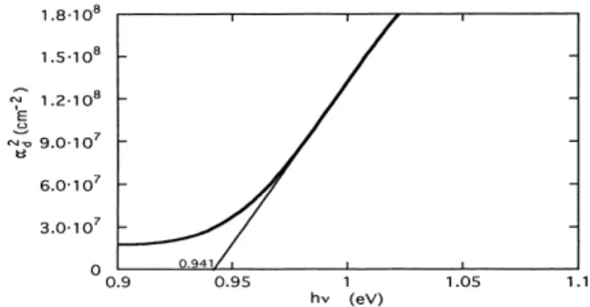
Figure 4. Dependence of the parameterα2
d on the photon
energy for a film deposited atTs= 100◦C.
Figure 3(a) shows the transmission of a substrate, figure 3(b) a substrate with a CuInTe2 thin film on it and
figure 3(c) a CuInTe2 film only.
It is known that the fundamental absorption for CuInTe2
is due to allowed direct transitions [8–11]. The absorption coefficient αd for direct transitions is defined by the
following relation [21, 22] αd = A∗(hγ − Eg)1/2 where A∗= Cm∗3/2r /n and C= πe223/2/ch2m∗eε0
is a constant, where m∗r is the effective reduced mass and
nis the index of refraction.
From the plot of α2d versus hν (figure 4) we have
determined the energy gap Eg ≈ 0.94 eV. This is
in agreement with literature data [8, 10–12]. We have determined also A∗2 (the slope of α2
d versus hν), i.e. A∗2 = 2.3 × 10⁹ (eV cm2)−1; this value compares well
with the published values for CuInSe2[23] and GaAs [24].
Based upon a value of n≈ 2.6 [25] for thin films, the deduced value of the effective reduced mass m∗r is 0.07me,
(m∗−1r = m∗−1e + m∗−1h ).
The absence of a sharp absorption edge (figure 4) can be attributed to the presence of binary compounds on the surface of the films. This is in accordance with 1660
Characterization of CuInTe2thin films prepared by flash evaporation
the GIXD measurements which are performed at the x-ray incidence angle β= 0.25◦. However, no binary phases are detected with this technique in the volume of the samples as demonstrated by the XRD measurements.
4. Conclusion
CuInTe2thin films have been deposited by flash evaporation
at different substrate temperatures. Films deposited on unintentionally heated substrates were amorphous. At substrate temperatures greater than 100 ◦C the GIXD spectra, taken at different incidence angles on the films, demonstrate the existence of the characteristic peaks of the chalcopyrite structure and the presence of the binary
compounds on the surface of the films. However,
in the volume no phase of any binary compounds or elemental components was detected by XRD. From the x-ray reflectometry spectrum we have determined the density of the CuInTe2 thin film, i.e. ρ≈ 6 g cm−3.
Electrical measurements demonstrate that the films were p type with a resistivity in the range of 0.3–2 cm for films deposited at Ts= 100◦C.
From the optical measurements on the CuInTe2 film
prepared by flash evaporation at a substrate temperature
Ts= 100◦C we have determined both the energy gap Eg≈
0.94 eV and the effective reduced mass m∗r ≈ 0.07me.
Acknowledgments
The authors would like to thank Professor R Evrard (Universit´e de Li`ege, Belgique), Professor A Bennouna and Dr Y Ijdiyaou (Universit´e Cadi Ayyad, Morocco) for help in this investigation.
References
[1] Shay J L and Wernick J H 1975 Ternary Chalcopyrite
Semiconductors, Growth, Electronic Properties and Applications (New York: Pergamon)
[2] Mass´e G and Djessas K 1993 Phys. Status Solidi a 139 K45 [3] Rockett A, Abou-Elfotouh F, Albin D, Bode M, Ermer J,
Klenk R, Lommasson T, Russell T W F,
Tomlinson R D, Stolt J, Walter T and Peterson T M 1994 Thin Solid Films 237 1–11
[4] Tuttle J R, Contreras M A, Gillespie T J, Ramanathan K R, Tennant A L, Keane J, Gabor A M and Noufi R 1995
Prog. Photovolt. 3 235–8
[5] Tuttle J R, Contreras M A, Gabor A M, Ramanathan K R, Tennant A L, Albin D S, Keane J and Noufi R 1995
Prog. Photovolt. 3 383–91
[6] Mitchell K W, Eberspacher C, Ermer J H, Pauls K L and Pier D N 1990 IEEE. Trans. Electron. Devices
37 410
[7] Tell B, Shay J L and Kasper H M 1972 J. Appl. Phys. 43 2469
[8] Wasim S M and Albornoz J G 1988 Phys. Status Solidi a
110 575
[9] Chahboun N, El Assali K, Khiara A, Ameziane E L and Bekkay T 1994 Solar Energy Mater. Solar Cells
32 213
[10] Thwaites M J, Tomlinson R D and Hampshire M J 1977
Solid State Commun. 23 905
[11] Joshi N V and Aguilar H 1982 J. Phys. Chem. Solids 43 792
[12] Horig W, Neumann H, Savelev V, Lagzdonis J, Schuman R, Kuhn G 1989 Cryst. Res. Technol.
24 823
[13] Sethi B R, Dashtiani M, Sharma O P and Mathur P C 1992
Phys. Status Solidi a 134 151
[14] Lokhande C D and Pawar S H 1987 J. Phys. D: Appl.
Phys. 20 1213–4
[15] Mooney G D, Hermann A M, Tuttle J R, Albin D S and Noufi R 1991 Appl. Phys. Lett. 58 2678
[16] Aren G, Vankar V D, Agnihotri O P and Singh C 1992
J. Appl. Phys. 72 3659
[17] Tuttle J R, Sites J R, Delahoy A, Shafarman W, Basol B, Fonash S, Gray J, Menner R, Phillips J, Rockett A, Scofield J, Shapiro F R, Singh P, Suntharalingam V, Tarrant D, Walter T, Wiederman S and Peterson T M 1995 Prog. Photovolt. 3 89–104
[18] Bennouna A, Laaziz Y and Idrisssi M A 1992 Thin Solid
Films 213 55
[19] Fiedenhans R 1989 Surf. Sci. Rep. 10 105
[20] Sridevi D and Reddy K V 1986 Thin Solid Films 141 [21] Bardeen J, Blatt F J and Hall L H 1954 Proc. Atlantic City
Photoconductivity Conf. (New York: Wiley) p 146
[22] Pankove J I 1971 Optical Processing in Semiconductors (New York: Dover) p 36
[23] Tuttle J R 1990 Thesis University of Colorado, Boulder, CO
[24] Wang S 1987 Fundamentals of Semiconductor Theory and
Device Physics (Englewood Cliffs, NJ: Prentice-Hall)
p 607
[25] Boustani M, El Assali K, Bekkay T and Khiara A 1997
Solar Energy Materials and Solar Cells 45 369