211th ECS Meeting, Abstract #750, © The Electrochemical Society
Strained Silicon-On-Insulator – Fabrication and Characterization
M. Reiche 1), C. Himcinschi 1), U. Gösele 1), S.
Christian-sen 1), S. Mantl 2), D. Buca 2), Q.T. Zhao 2), S. Feste 2),
R. Loo 3), D. Nguyen 3), W. Buchholtz 4), A. Wei 4),
M. Horstmann 4) ,D. Feijoo 5), and P. Storck 5) 1) MPI für Mikrostrukturphysik, Halle, Germany 2) Forschungszentrum Jülich, Jülich, Germany 3) IMEC, Leuven, Belgium
4) AMD Saxony, Dresden, Germany 5) Siltronic AG, München, Germany
The benefits of enhanced carrier mobilities in strained silicon (sSi) and reduced parasitic capacitances in silicon-on-insulator (SOI) substrates have recently been
combined together in strained silicon-on-insulator (sSOI) technology. The sSOI substrates are of immense
importance for new generations of CMOS technology. Strained silicon layers about 20 nm thick were grown on virtual substrates characterized by a thin SiGe layer having a thickness of 400nm (Fig. 1). The SiGe layers were relaxed by hydrogen or helium implantation and subsequently annealed resulting in threading dislocation densities as low as 1105 cm-2 and dislocation
pile-up densities of 10 cm-1. The reduced thickness of the
SiGe buffer causes also a low surface roughness
compared to conventional SiGe virtual substrates having a few micrometer thick buffer layer [1]. Therefore,
additional planarization steps (CMP) for further treatments are not required.
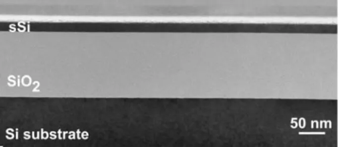
SSOI wafers were fabricated by hydrogen-induced layer splitting combined with wafer bonding techniques. The virtual substrates were implanted with hydrogen at energies ranging from 135 keV to 110 keV which leads to the maximum of the deposited energy being located either in the underlying Si substrate or at the interface between the SiGe layer and the Si handle wafer. The virtual substrates were bonded to Si wafers and subsequently annealed at a maximum temperature of 450°C (Fig. 2). The annealing causes an increase of the bond energy and the layer splitting. Finally, the SiGe layer was removed by wet chemical etching (Fig. 3). The integrity of the buried oxide layer was improved by an additional annealing step at high temperatures comparable to those used in device processes. Also a further epitaxial growth process was applied to increase the thickness of the strained silicon layer.
Analysis of the fabricated sSOI wafers (diameter 8 in.) show that the whole strain of the sSi layer is transferred. The strain is also unchanged after an additional annealing at elevated temperatures and an increase of the sSi layer thickness to 60 nm.
Long channel MOSFETs were fabricated on the sSOI substrates. Measurements of the electron mobility resulted in an enhancement of nearly 100 %. Also the on current showed a large improvement.
[1] S. Mantl, D. Buca, B. Holländer, St. Lenk, N. Hueging M. Luysberg, R. Carius, R. Loo, M. Caymax, H. Schäfer, I. Radu, M. Reiche, S. Christiansen, and U. Gösele, From thin relaxed SiGe buffer layers to strained silicon directly on oxide, ECS Transactions 3(7), 1057 (2006)
Fig. 1: TEM cross-sectional image of the virtual substrate. A 20 nm thick sSi layer was grown on a 400 nm thick SiGe buffer.
Fig. 2: Infrared microscope image of a bonded wafer pair.
Fig. 3: TEM cross-sectional image of the final sSOI wafer.