HAL Id: hal-00468141
https://hal.univ-brest.fr/hal-00468141
Submitted on 30 Mar 2010
HAL is a multi-disciplinary open access
archive for the deposit and dissemination of
sci-entific research documents, whether they are
pub-lished or not. The documents may come from
teaching and research institutions in France or
abroad, or from public or private research centers.
L’archive ouverte pluridisciplinaire HAL, est
destinée au dépôt et à la diffusion de documents
scientifiques de niveau recherche, publiés ou non,
émanant des établissements d’enseignement et de
recherche français ou étrangers, des laboratoires
publics ou privés.
Synthesis of Broadband Negative Group Delay Active
Circuits
Blaise Ravelo, André Pérennec, Marc Le Roy
To cite this version:
Blaise Ravelo, André Pérennec, Marc Le Roy. Synthesis of Broadband Negative Group Delay
Ac-tive Circuits. IEEE MTT-S International Microwave Symposium, Jun 2007, Hawaï, United States.
pp.2177-2180, �10.1109/MWSYM.2007.380357�. �hal-00468141�
Synthesis of Broadband Negative Group Delay Active Circuits
Blaise Ravelo, André Pérennec, Marc Le Roy and Yann G. Boucher
LEST– UMR CNRS 6165 – UBO/ENSTBr- CS93837, F-29238 Brest cedex 3, France.
RESO – EA3380 – CS72862, F-29238 Brest cedex 3, France.
Abstract — This paper deals with the design and synthesis of
active circuits that produce simultaneously negative group delay and gain at microwave frequencies or for baseband signals. For a single cell, analytical equations show that the proposed topology meets these objectives while also satisfying active device requirements. Then, a synthesis approach is extracted and applied to design a two stage microwave circuit which is validated by a comparison between simulation and experimental results. This method is extended to design a four-stage baseband active circuit that provides gain and negative group delay up to 1 GHz. Frequency and time-domain simulations illustrate the topology ability to achieve high relative time-advance.
Index Terms — Active device, FET circuits, negative group
delay, superluminal group velocity. I. INTRODUCTION
Materials with simultaneously or independently negative permittivity and permeability, initially introduced in the late 1960s by Veselago [1], are now validated in 3-D artificial media [2] and in 1-D or 2-D microwave circuits [3]. Much recently, such metamaterials also know as Left-Handed Media (LHM), has been applied, in microstrip and coplanar waveguide technologies, to design antennas, filters, couplers [4], phase shifters[5]. In general, in these devices, the LHM properties are used either to reduce the circuit size or to enlarge the initial operating bandwidth.
In 1960, the classical analysis of Brillouin and Sommerfeld [6] showed that in a frequency band of anomalous dispersion, e.g. obtained from electromagnetic Bragg gratings [7] or metamaterials, the group velocity can become greater than the speed of light in vacuum c, or even be negative. Since 1999, a renewed interest for the “superluminal” group velocity has emerged and this counter-intuitive effect has been widely debated [8]. It is well confirmed now that this behavior is not at odd with causality, and most points of controversy have been settled down. However, to illustrate and establish the properties of this intriguing phenomenon, several configurations or experimental circuits exhibiting Negative Group Delay (NGD) or superluminal phenomenon have been proposed [9]-[10]. These devices can be merged in two major categories. The first one essentially devoted to microwave applications consists in LHM built with the passive left-handed cell [3], i.e. a series capacitance and a shunt inductance, associated with a RLC parallel-resonant network. To achieve a significant NGD value, many cells have to be cascaded resulting in a very low transmission level.
The second category brings together experiments with NGD or Negative Refractive Index (NRI) with an amplification of the input signal or, at least, loss compensation. In the most debated one [8], a region of anomalous dispersion is created in a kind of optical amplifier, and the authors measured a group velocity of – c/310. All the other active NGD circuits only operate for baseband signals under a few hundred of KHz and are based on a simple electronic circuit built with an operational amplifier, a resistor and a capacitor [9]-[10]. Gain and high relative advances of a Gaussian baseband signal can be achieved by cascading several stages. Such simple electronics circuits are very useful to analyze the properties of superluminal group velocity; but nevertheless, they are fairly narrowband and restricted to low frequencies.
This assessment led us to investigate for a more general approach that should bring of course NGD, gain, thus necessarily active, and should operate for broad and base-band signals as for modulated ones over the microwave domain. Section II will describe the proposed topology and the theoretical analyze of its S-parameters. Section III compares the simulated and measured frequency results of a two stages NGD active device. In section IV, a broadband synthesis method is developed from the initial cell equations. Then, frequency and time-domain simulations of a broadband and baseband NGD active circuit of four stages are presented and we discuss on limitations and improvements of this circuit.
II. PROPOSED NGDTOPOLOGY AND SYNTHESIS EQUATIONS Here, the more global notion of group delay is to be used instead of group velocity because it is well defined both for lumped circuits, and for distributed ones. Generally, the group delay, τ = -dϕ/dω, is extracted from experimental S-parameters, where ϕ is the frequency-dependent transmission phase shift and ω is the angular frequency. In the case of a frequency limited bandwidth input signal, the group delay corresponds to the time shift of its envelope maximum. We though that a Field Effect Transistor (FET) associated with passive components could bring promising possibilities to achieve our severe objectives; i.e. NGD, gain, input and output matching, low noise and stability.
2 Intuitively, we first tested several configurations of the classical LHM cell [3] which provides by itself NGD, in cascade or in parallel with a FET. But finally, the topology depicted in Fig. 1, compared to those with LHM cells, proposes simultaneously higher significant NGD and gain values, a higher simplicity, and moreover a possibility of input/output matching. It consists in a series RLC resonant circuit in shunt at the FET drain output.
FET
C L R
Fig. 1. Series RLC resonant network in cascade with a FET. To allow an analytical description of the cell, the FET is modeled by a voltage-controlled current generator and RDS,
the drain-source resistor. The group delay, τ, is negative at the
RLC network resonance frequency ω 0=1/ LCand at this
particular frequency: ) ( 2 ) ( 0 0 0 21 ds ds ds m R R Z R R R g RZ S + + − =
ω
(1) )] ( .[ 2 ) ( 0 0 0 ds ds ds R R Z RR R R LZ + + − = ω τ (2) ) ( ) ( ) ( 0 0 0 22 ds ds ds ds R R Z R R R R Z R R S + + + − =ω
(3)where Z0 is the input impedance of the reference ports
(50 Ω in practice) and gm is the FET transconductance. A few
remarks must be underlined:
- S12 is null and S11 is close to one at low frequency;
- the group delay is always negative at the cell resonance; - (3) shows that an output matching is possible;
- a significant gain value can be obtained even if it is minimum at the resonance; R must be small to get a significant NGD value but this implies a low transducer gain; - S21, τ, and ω 0 do not depend of exactly the same parameters,
so it means that τ can be controlled independently from S21
through L and that the resonance frequency can be changed via C without modifying the level of τ ; and thus, this gives us degrees of freedom to find a satisfying compromise.
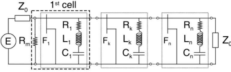
B. The whole circuit synthesis
Surprisingly, this topology is that of a resistive amplifier, excepted for the components values. To match the circuit input, a shunt resistor, Rm, is placed between the first cell and
the generator (Fig. 2).
Z
0C
nL
n Rn FnC
kL
k Rk FkC
1L
1 R1 F1Z
0 E Rm 1stcellFig. 2. Structure of the n-stages cascaded ideal circuit. Then, considering this resistor and the following unit cell as a new first cell, the group delay (2) and S22 (3) expressions are
not modified, but the other significant parameters are now defined by: 0 0 1 11( ) R Z Z R S m m + − = ω (4) ) )( ( 2 ) ( 1 1 0 0 0 0 1 1 21 ds ds m ds m m R R R Z R Z Z R R g Z R R S + + + − = ω (5)
where ω1 is the R1L1C1 resonant angular frequency. For a
relatively high value of Rm, the first stage masks the noise
brought back by a possible low value of R1. To synthesize the network component values, we define the objectives for the synthesis of the first cell and Rm as followed:
a
S11(
ω
1) = ,S21(ω
1) =bandτ
(ω
1)=τ
1. Then, by simplyinverting (3), (4) and (5), we obtain:
a a Z Rm − + = 1 1 0 (6) )] ) ( ( 2 [ ) ( 0 2 0 0 0 ds m ds m ds m m m ds 0 1 R R R R Z Z b R R Z g Z R R b.Z R + + + − + = (7) ds ds ds R Z R R Z R R R L 0 1 0 1 1 1 1 2 )] ( [ . + + − = τ and 2 1 1 1 1 ω L C = . (8)-(9) For a unit cell k, and at the series resonance frequency ωk,
only the expression of Rk is different:
)] ( 2 [ m 0 ds 0 ds ds 0 k R Z b R Z g R bZ R + − = . (10)
Obviously, Rk plays also the part of inter-stage matching
impedance. To choose an appropriate transistor, particularly through gm, and to obtain the S22(ω1) = c objective, the four
following equations may also be used for the first cell:
a a Z Rm − + = 1 1 0 (1 )(1 ) 2 0 a c Z b gm= + + (11)-(12) ) ( ) 1 ( 0 0 ds ds ds 0 1 R Z cZ R c R Z R + − − + = 2 0 0 2 0 1 1 [ ( )] ) 1 ( ds ds ds R Z c R Z c R Z L + + − + − = τ (13)-(14)
C1 is still defined as in (9). Obviously, these synthesis equations are only valid for the simple microwave low frequency model, but they provide component values really close to final values achievable through optimization with a more complete modelization.
III.EXPERIMENTAL VALIDATION AND NGD CIRCUIT IMPLEMENTATION
In order to validate the theory, we chose to build a circuit working around 1 GHz. Moreover, we initially limited ourselves to a two stages design with identical resonance frequencies. In that case, from either the classical transducer gain formulas or by cascading chain matrices of cells defined in the previous section, we obtain for the total insertion loss:
(
1)(
0)(
2 0 0 2)
0 2 1 2 2 11 22 21 21 21 2 1 1 2 2 1 R R R Z Z R R Z R R R Z R R R g S S S S S ds ds m ds m ds m T = − = + + + + (15)As the FETs are unilateral, S11T can be identified as the return
loss of the first cell (4) and S22T to the output return loss of the
second one (3). The objectives were that S11T and S22T were
below -10 dB, a theoretical total gain around 6 dB and a NGD better than -2 ns. We searched for a FET with high gm and RDS
values. Then, we got R2 from (10) and Rm from (11). For the
specified frequency, initially 1.45 GHz, C1 and C2 were
chosen identical and small to allow L1 and L2 to be sufficiently
high to achieve a significant NGD. Thanks to R1, a -1.66 ns
NGD is achieved for the first cell and due to the R2 low value,
only -0.33 ns for the second stage and then each S21 stage
parameter can be evaluated, i.e. 10.84 dB and 0.06 dB for the first and second respectively. Finally, we achieve, in theory, a total transmission gain of 6 dB and a matching of -14 dB at the input and -11 dB at the output with a -2.3 ns group delay. The total group delay is not simply equal to the sum of each stage one due to the Z0 reference of the S-parameters at their
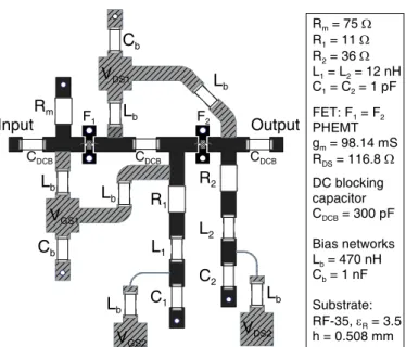
interface. All the circuit references are summarized in Fig. 5. The S-parameters and the group delay remain practically unchanged when a high frequency equivalent circuit model is introduced. On the other hand, when the connection microstrip lines and the real passive components models are introduced in the schematic or electromagnetic simulations, the operating frequency is shifted down to 1.07 GHz and S21T
is reduced to 3 dB. Fig. 5 shows the layout of the final circuit. Two different bias networks has been implemented, a conventional one (VGS1 and VDS1 for gate and drain biases),
and a second network (VGS2 and VDS2) which is connected
through the resonant cells and they both give identical measurement results. Fig 6-a and 6-b show a good agreement between electromagnetic simulations and experimental results (obtained with no adjustment). The measured group delay is of -2.3 ns at 1.03 GHz while the S21T parameter is 1.68 dB. At
this specific frequency, S11T is around -14 dB and S22T below
-12 dB. C1 R1 F1 Rm C2 L2 R2 F2 Lb Lb Lb Lb Lb L b Cb Cb CDCB Input Output CDCB CDCB L1 VGS1 VGS2 VDS1 VDS2 Rm = 75 Ω R1 = 11 Ω R2 = 36 Ω L1 = L2 = 12 nH C1 = C2 = 1 pF FET: F1 = F2 PHEMT gm = 98.14 mS RDS = 116.8 Ω DC blocking capacitor CDCB = 300 pF Bias networks Lb = 470 nH Cb = 1 nF Substrate: RF-35, εR = 3.5 h = 0.508 mm
Fig. 5. Microstrip circuit layout in black, bias networks layout in hatched gray (White circles indicate ground via-holes) and component references. 0.8 0.9 1.0 1.1 1.2 1.3 1.4 1.5 1.6 0.7 1.7 -18 -16 -14 -12 -10 -8 -20 -6 Frequency (GHz) S1 1T (dB), S 22T (dB) Simulations Measurements S22T S11T 0.8 0.9 1.0 1.1 1.2 1.3 1.4 1.5 1.6 0.7 1.7 5 10 15 20 25 30 35 0 40 -5 -4 -3 -2 -1 0 1 -6 2 Frequency (GHz) S21T ( dB) G rou p D ela y (n s) Simulations Measurements
Fig. 6. Comparison of simulated and measured S-parameters and group delay. (a) Input and output return losses. (b) S21 parameters
and group delay.
Compared to previous studies with passive components [3], we achieve slightly higher NGD and bandwidth values for an equivalent number of cells. The possibility of each stage characteristics to be controlled independently and particularly the resonance frequencies brings opportunity to propose the synthesis of a broadband NGD circuit.
(a)
4 IV. DESIGN OF A BROADBAND NGD ACTIVE CIRCUIT FOR
BASEBAND SIGNALS
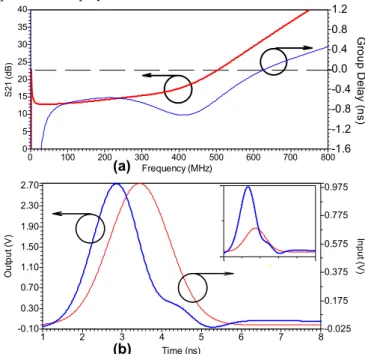
In digital transmission domain and for high data rates, the ideal characteristic of a NGD active circuit would be a constant phase advance and gain over the entire signal wide bandwidth. Fortunately, in many applications, the digital signal is filtered to frequency limit its spectrum. So, we will restrict our goal to the bandwidth that minimize the intersymbol interferences of a gaussian baseband signal and thus keep as low as possible signal distortions, ripples and pulse reshaping. With the topology presented in section II, a NGD broadband has been achieved with a 4 stage circuit. Each stage component values have been calculated separately for resonant frequency regularly spread from 0 to 600 MHz and the whole circuit behavior has been predicted from the sum of the stage transfert functions for the gain and by the sum of the time delay of these transfert functions (instead pof S-parameters) for the total group delay. A final optimization and electromagnetic simulations have been performed in the same conditions as in section IV (Fig. 7-a), i.e. with the component S-parameters, the interconnection lines and the bias network, and with the same FET and substrate. For such a broadband, an active bias network had to be implemented. Time-domain simulations (Fig. 7-b) are also presented and exhibit a relative time advance of 82 % compare to the 0.7 ns standard deviation. A pulse compression is also evidenced, particularly in the inset of fig.7-b where the input and output pulses are displayed on a same ordinate scale.
Frequency (MHz) 100 200 300 400 500 600 700 0 800 5 10 15 20 25 30 35 0 40 -1.2 -0.8 -0.4 0.0 0.4 0.8 -1.6 1.2 S 21 ( dB ) G roup D e la y ( ns) 2 3 4 5 6 7 1 8 0.30 0.70 1.10 1.50 1.90 2.30 -0.10 2.70 0.175 0.375 0.575 0.775 -0.025 0.975 Time (ns) In p ut ( V ) Ou tp u t (V )
Fig. 7. Simulated S21 parameter and group delay (a). Time-
domain simulations (b). Rm = 75 Ω, R1 = R2 = 10 Ω, R3 = 18 Ω, R4 =
30 Ω, C1 = 150 nF, C2 = 3.9 nF, C3 = 11 pF, C4 = 2.7 pF, L1 = L2 =
3.6 nH, L3 = 8.7 nH, L4 = 8.2 nH.
V. CONCLUSION
We report on a new NGD active topology that provides simultaneously gain and NGD. To validate our theoretical results, we have designed and implemented a two stage circuit for microwave frequency modulated signals. Analysis and synthesis equations are proposed and are sufficiently general to be applied to several frequency bands. Moreover, a few numbers of cells lead to significant gain and relative time-advance values. Indeed, we simulated in frequency and in time-domain a four-stage circuit that provided gain and a negative delay even for a broadband and baseband Gaussian input signal. This proposal brings some prospects for applications in the communication domains. Time-domain measurements are scheduled to verify the time advance sensibility versus noises and mm-waves distributed circuits are also planed.
REFERENCES
[1] V. Veselago, “The electrodynamics of substances with simultaneously negative values of ε and µ,” Soviet Physics Uspekhi, vol. 10, no. 4, pp. 509-514, 1968.
[2] R. A. Shelby D. R. Smith, and S. Schultz, “Experimental verification of a negative index of refraction,” Science, vol. 292, no. 5514, pp. 77-79, Ap. 2001.
[3] O. F. Siddiqui, M. Mojahedi, G. V. Eleftheriades, ”Periodically Loaded Transmission Line With Effective Negative Refractive Index and Negative Group Velocity”, IEEE Trans. Antennas Propagat., vol. 51, No. 10, Oct. 2003.
[4] A. Lai, C. Caloz, and T. Itoh, “Composite right/left-handed transmission line metamaterials”, IEEE Microwave Magazine, vol. 5, pp. 34 – 50, Sept. 2004.
[5] M. A. Antoniades, and G. V. Eleftheriades, “Compact linear lead/lag metamaterial phase shifters for broadband applications,” IEEE Antennas and Wireless Propagation Letters, vol. 2, 103, July 2003.
[6] L. Brillouin, and A. Sommerfeld, Wave Propagation and Group Velocity, Academic Press, New York, 1960, pp. 113-137. [7] M. Le Roy, E. Lheurette, A. Pérennec : “Pulse Compression
with Superluminal Group Velocity in 1-D Photonic Bandgap Coplanar Waveguide”, Proc. 34 th European Microwave Conf., Amsterdam, Oct. 2004, pp. 463-466.
[8] L. J. Wang, A. Kuzmich and A. Dogariu, “Gain-Assisted Superluminal Light Propagation”, Nature 406, pp. 277-279, June 2000.
[9] D. Solli, R.Y. Chiao, “Superluminal effects and negative delays in electronics, and their applications”, Physical Review E, Issue 5, Nov. 2002.
[10] M. Kitano, T. Nakanishi, K. Sugiyama, “Negative Group Delay and Superluminal Propagation: An Electronic Circuit Approach”, IEEE Journal of Selected Topics in Quantum Electronics, vol.9 No. 1, p. 43, 2003.
(a)