Université de Montréal
Templating gold nanoparticles on nanofibers
using block copolymer thin films
par Hu Zhu
Département de chimie Faculté des arts et des sciences
Thèse présentée à la Faculté des études supérieures et postdoctorales en vue de l’obtention du grade de
Philosophiae Doctor (Ph.D.) en chimie
Septembre 2018
i
Résumé
Les nanocapteurs à diffusion Raman exaltée par effets de surface (SERS) basés sur les nanofibres sont une des technologies prometteuses pour les études cellulaires. Une approche ascendante de nanofabrication des nanofibres reposant sur l'auto-assemblage électrostatique des nanoparticules d'or (AuNPs) chargées avec un film portant des charges opposées qui recouvre la nanofibre est proposée. Les revêtements courants tels que les monocouches auto-assemblées d'alcoxysilanes et les films d'homopolymère souffrent de l'agrégation des AuNPs et d'inhomogénéités. Des gabarits de film en copolymère à bloc (BCP) ayant des motifs de surface bien définis peuvent guider le dépôt ordonné des réseaux d’AuNPs, mais ont été étudiés presque exclusivement sur des substrats plats. L’objectif principal de cette thèse a été de revêtir les nanofibres avec des BCP dans le but d'obtenir des réseaux d’AuNPs denses et uniformes sur la nanofibre.
Pour y parvenir, des fibres de verre étirées ayant des diamètres allant jusqu'à 100 nm ont été trempées dans des solutions de polystyrène-bloc-poly(4-vinylpyridine) (PS-b-P4VP) dans le THF à différentes concentrations et taux d'enduction. On a constaté que seul un film de type brosse ayant une épaisseur d'environ 3 nm est obtenu sur la nanofibre. Ce film se forme par adsorption où le bloc P4VP ancre le BCP à la surface polaire de la nanofibre de verre via de multiples liaisons hydrogène alors que le bloc PS est exposé à la solution. L'incubation de la nanofibre recouverte de la brosse dans des colloïdes aqueux d'AuNPs entraîne un dépôt d'AuNPs dense et bien dispersé. En revanche, les films de l'homopolymère, P4VP, et d'un copolymèrestatistique, PS-s-P4VP, présentent une certaine agrégation des AuNPs, indiquant un effet de barrière stérique créée par les blocs du PS. Une augmentation de la rugosité de la brosse a été observée après l’immersion dans l'eau, ce qui indique que le dépôt des AuNPs a conduit à un réarrangement local des chaînes du PS pour exposer des portions des chaînes P4VP afin d’attirer les AuNPs. De même, en suivant la cinétique d’adsorption en mesurant l’épaisseur du film sec en fonction du temps d’adsorption, on a constaté que les films saturés avaient une morphologie lisse (obtenue après 2 minutes d’adsorption) et que les films insaturés avaient une morphologie plus
rugueuse; cependant, cette dernière n’a pas modifié les caractéristiques de dépôt des AuNPs.
Pour une meilleure compréhension, les mêmes films PS-b-P4VP ont été étudiés sur des surfaces planes. L'effet de la courbure de surface s'est avéré similaire à l'effet de la concentration de la solution de polymère, avec une évolution similaire de la morphologie du film pour une concentration décroissante et un diamètre de fibre décroissant, à savoir d'une morphologie de type micellaire à une morphologie partiellement micellaire et partiellement brosse et, finalement, à une morphologie brosse. Alors que cette dernière conduit à un dépôt d'AuNPs denses et bien dispersées, la morphologie micellaire conduit à des petites grappes d'AuNPs (pour de petites AuNPs). Enfin, il a été démontré que les nanofibres peuvent être recouvertes par des BCPs chargés d’ions en utilisant des techniques de revêtement en goutte. En ce qui concerne les applications de l'optophysiologie SERS, la nanofibre revêtue d’AuNPs denses et bien dispersées grâce au BCP en brosse s'est révélée, par la détection in vitro des neurotransmetteurs, plus performante.
Mots-clés: SERS, nanofibres, couches minces, copolymères à blocs,
polystyrène-bloc-poly(4-vinylpyridine), couches de type brosse, adsorption, trempage, courbure du
iii
Abstract
Surface enhanced Raman scattering (SERS) nanosensors based on pulled nanofibers are a promising technology for cellular studies. A bottom-up nanofabrication approach towards SERS nanofibers is based on electrostatic self-assembly of charged gold nanoparticles (AuNPs) with a film carrying opposite charges that coats the nanofiber. Common coatings such as self-assembled monolayers of alkoxysilanes and homopolymer films suffer from AuNP aggregation and inhomogeneities. Block copolymer (BCP) film templates having surface patterns can guide the ordered deposition of AuNP arrays, but have been investigated almost exclusively on flat substrates. A major objective of this thesis is to coat nanofibers with BCPs with the aim of achieving uniform AuNP arrays on the nanofiber.
To achieve this, pulled glass fibers with sub-micron tip diameters were dip-coated from polystyrene-block-poly(4-vinylpyridine) (PS-b-P4VP) solutions in THF of various polymer solution concentrations and dip-coating rates. It was found that only a brush film with a thickness of about 3 nm was obtained on the nanofiber. The brush film forms by adsorption, where the P4VP block anchors the BCP on the polar surface of the glass nanofiber via multiple H-bonds and the PS block dangles into the solution. Incubating the BCP-coated nanofiber in aqueous AuNP colloids leads to the deposition of dense and well-dispersed AuNPs on the nanofibers. In contrast, P4VP homopolymer and PS-s-P4VP random copolymer films show significant AuNP aggregation, indicating a steric barrier effect provided by the PS blocks. An increase in roughness of the BCP brush film was shown after immersion in water, indicating that the AuNP deposition results from local PS chain rearrangement to expose portions of the P4VP chains for attracting AuNPs. Similarly, when following the adsorption kinetics by measuring the dry film thickness as a function of adsorption time, it was found that saturated films had a smooth morphology (achieved within two minutes of adsorption) and unsaturated films exhibited a rougher morphology, but this did not change the deposition pattern of the AuNPs.
For greater understanding, the same dip-coated PS-b-P4VP films were studied on flat surfaces. The effect of surface curvature (fiber diameter) was found to parallel that of changing polymer solution concentration, as indicated by a similar film morphology evolution between decreasing polymer solution concentration and decreasing fiber diameter. Notably, it changes from a full micellar morphology to a mixed morphology of micelles and the brush layer (dewetting) to a full brush layer. While the featureless brush films led to dense and well dispersed AuNP deposition, the dots led to small AuNP clusters for AuNP diameters of about 10 nm. Finally, it was shown that nanofibers can be coated with gold ion-loaded BCPs using drop-coating techniques. In terms of applications in SERS optophysiology, the BCP brush-coated nanofiber with well dispersed AuNP deposition was shown to give a superior performance, as shown by in vitro detection of neurotransmitters.
Keywords: SERS, nanofibers, thin films, block copolymers,
polystyrene-block-poly(4-vinylpyridine), block copolymer brush layers, block copolymer adsorption, dip-coating, substrate curvature, gold nanoparticles, self-assembly.
v
Table of contents
Résumé... i Abstract ... iii Table of contents ... v List of tables ... x List of schemes ... xiList of figures ... xii
List of symbols and abbreviations... xxi
Acknowledgements ... xxiv
Chapter 1. Introduction ... 1
1.1 Localized surface plasmon resonance (LSPR) ... 2
1.2 Surface enhanced Raman scattering (SERS) ... 4
1.3 SERS nanoprobes for single cell studies ... 7
1.3.1 Platforms for constructing SERS nanoprobes ... 8
1.3.2 Detection using SERS nanoprobes ... 10
1.3.3 Fabrication of SERS nanoprobes ... 11
1.4 Block copolymer self-assembly... 14
1.4.1 Microphase separation of diblock copolymers ... 14
1.4.2 Block copolymer thin films ... 16
1.4.3 Fabrication of NP arrays using BCP film templates ... 17
1.5.1 “V” relationship in dip-coating ...27
1.5.2 Substrate curvature effect in dip-coating ...28
1.6 Adsorbed block copolymers ...29
1.6.1 Adsorbed homopolymer films ...29
1.6.2 End-grafted polymer brush ...30
1.6.3 Block copolymer adsorption ...33
1.7 Scope of the thesis ...37
1.8 Structure of thesis ...40
1.9 References ...41
Chapter 2. Block Copolymer Brush Layer-Templated Gold Nanoparticles on Nanofibers for Surface Enhanced Raman Scattering Optophysiology ...52
2.1 Abstract...52
2.2 Introduction ...53
2.3 Experimental...54
2.3.1 Methods ...54
2.3.2 Block copolymer solution preparation and dip-coating ...55
2.3.3 Gold nanoparticle (AuNP) synthesis and deposition ...55
2.3.4 Scanning electron microscopy (SEM) ...56
2.3.5 Atomic force microscopy (AFM) ...56
2.3.6 Surface enhanced Raman spectroscopy (SERS) ...57
2.3.7 Finite element method simulations ...57
2.3.8 SERS optophysiology near dopaminergic neurons ...57
2.4 Results and discussion ...60
vii
2.6 Supporting information ... 77
2.7 References ... 89
Chapter 3. Monolayer Arrays of Nanoparticles on Block Copolymer Brush Films ... 93
3.1 Abstract ... 93
3.2 Introduction ... 94
3.3 Experimental ... 97
3.3.1 Materials ... 97
3.3.2 Block copolymer solutions ... 98
3.3.3 Dip-coating ... 98
3.3.4 AuNP synthesis and deposition ... 99
3.3.5 Atomic force microscopy (AFM)... 99
3.3.6 Spectroscopic ellipsometry ... 100
3.3.7 Scanning electron microscopy (SEM) ... 100
3.3.8 Water contact angle measurements ... 100
3.4 Results and discussion ... 101
3.4.1 Effect of polymer solution concentration on the BCP film pattern and the AuNP distribution ... 101
3.4.2 Relationship between dip-coating rate, polymer solution concentration, film thickness and film morphology ... 106
3.4.3 Adsorbed block copolymer nanolayers for templating AuNPs... 108
3.5 Conclusions ... 118
3.6 Supporting Information ... 119
Chapter 4. Templating Gold Nanoparticles on Nanofibers with Block Copolymer Brush Layers ...135 4.1 Abstract...135 4.2 Introduction ...136 4.3 Experimental...139 4.3.1 Materials...139 4.3.2 Glass fibers ...140
4.3.3 Block copolymer solution preparation and dip-coating ...141
4.3.4 AuNP synthesis and deposition...141
4.3.5 Scanning electron microscopy (SEM) ...142
4.3.6 Atomic force microscopy (AFM) ...142
4.4 Results and discussion ...142
4.4.1 Effect of curvature on BCP coatings of pulled fibers ...142
4.4.2 Investigation of various parameters governing the AuNP deposition on BCP brush-coated fibers ...147
4.5 Conclusions ...156
4.6 Supporting information ...158
4.7 References ...187
Chapter 5. Drop-Coating of Block Copolymer Self-Assembly Thin Films on Highly Curved Surfaces ...191 5.1 Abstract...191 5.2 Introduction ...191 5.3 Experimental...193 5.3.1 Materials...193 5.3.2 Glass fibers ...193
ix
5.3.3 Block copolymer solution preparation ... 193
5.3.4 Drop coating ... 194
5.3.5 Scanning electron microscopy (SEM) ... 194
5.4 Results and discussion ... 195
5.4.1 Theory of static drop-coating ... 195
5.4.2 Coating with a static drop ... 196
5.4.3 Coating with a flowing drop ... 201
5.5 Conclusions ... 204
5.6 References ... 204
Chapter 6. Conclusions and Perspectives ... 207
6.1 General conclusions ... 207
6.1.1 SERS optophysiology probes via BCP brush films ... 207
6.1.2 Two distinct layers in dip-coated block copolymer films ... 209
6.1.3 Effect of substrate curvature on the thickness of dip-coated BCP films... 211
6.1.4 Novel drop coating method for coating nanofibers... 213
6.2 Limitations ... 213
6.2.1 Thickness measurement on cylindrical surfaces ... 213
6.2.2 Brush films on highly curved surfaces ... 214
6.3 Perspectives ... 214
6.3.1 Solvents ... 214
6.3.2 Molecular characteristics ... 216
6.3.3 Applications ... 217
List of tables
Table 2.S1. Wavenumbers and Band Assignments of the Main Bands in the SERS
Spectra of Fig. 2.3. ...84
Table 3.1. Water Contact Angles of Films Subjected to the Static Immersion
Times Indicated. ...105
Table 3.S1 Detailed Analysis of Total Exposure Times of the Substrates to the
BCP Solution, Relevant to the Thickness Data for the Brush-Layer (Dot-Free) Films Shown in Figure 3 of the Main Text.. ...126
Table 4.1 Molecular characteristics of the PS-b-P4VP block copolymers (BCPs)
used and the density of 20-nm AuNPs deposited on the BCP coatings at a fiber diameter of about 10 µm. ...140
xi
List of schemes
Scheme 5.1. Representation of partial wetting and complete wetting of a liquid drop
on both flat substrate and cylindrical substrates ... 195
Scheme 5.2. Schematic illustration of the coating procedure by using the
spontaneus wetting film generated from a static drop of polymer
solution ... 197
Scheme 6.1. Schematic illustration of an AuNP-decorated nanofiber by using a
PS-b-P4VP brush film template adsorbed on the glass surface of the fiber 208
Scheme 6.2. Schematic illustrating the two layers structure of a PS-b-P4VP
dip-coated film and the deposition of small AuNPs on different types of films ... 211
Scheme 6.3. Schematic illustration of the similar effect between decreasing polymer
concentration and increasing substrate curvature on the thickness of BCP films, the nature of the film, and the pattern of small AuNPs
deposited on the film ... 212
List of figures
Figure 1.1. A Lycurgus cup and an illustration of LSPR sensing ...2 Figure 1.2. Schematic depiction of localized surface plasmons of metal
nanospheres...3
Figure 1.3. Jablonski diagram representing quantum energy transitions at a
molecular level for Rayleigh and Raman scattering. ...4
Figure 1.4. Schematic illustration of a “hot spot” for a NP dimer and the rapid
change in SERS enhancement factors with respect to relative position ...6
Figure 1.5. Intracellular SERS sensing with a SERS nanopipette ...8 Figure 1.6. Various nanoprobes that have been used as platforms for SERS
sensing ...9
Figure 1.7. SERS spectra collected from a variety of cells with the SERS
nanopipette ...11
Figure 1.8. Different types of interactions between aminosilane molecules and
silicon dioxide substrates and the structural irregularities in the
aminosilane-derived layer. ...12
Figure 1.9. Chemical structures of some common diblock copolymers ...14 Figure 1.10. Self-consistent mean-field theoretical phase diagram of diblock
copolymers at equilibrium in the melt and schematic illustration of some equilibrium morphologies depend on the block volume fraction ...15
Figure 1.11. Schematic representation of microphase-separated BCP thin film
patterns and the pattern transfer to the underlying substrate by using BCP films as photolithographic masks ...17
Figure 1.12. Guided deposition of AuNP clusters arrays using BCP thin films:
schematic illustration, TEM images and SERS results ...19
Figure 1.13. Guided deposition of single AuNP arrays using BCP thin films:
schematic illustration, AFM and SEM images, and SERS results ...21
Figure 1.14. Back-filling method for the deposition of AuNPs using BCP thin
xiii
Figure 1.15. In situ synthesis of NPs in BCP thin films by galvanic displacement
process: schematic illustration and SEM images ... 24
Figure 1.16. Ordered arrays of NPs using BCP films composed of metal ion
preloaded micelles: shematic illustration and SEM images ... 26
Figure 1.17. Schematic illustration of BCP film formation in the capillarity and
draining regimes during dip-coating and the V-shape relationship
between film thickness and dip-coating rate... 28
Figure 1.18. Relation between film thickness and capillary number for dip-coating
fibers of various radii with coating solutions of various viscosities ... 29
Figure 1.19. Shematic illustration of tails, loops and trains in a homopolymer chain
physically adsorbed on a surface ... 30
Figure 1.20. Schematic illustrations of mushroom, pancake and brush structures of
chemically end-grafted polymer chains ... 31
Figure 1.21. Nanopatterns in end-grafted homopolymer film of different grafting
density: schematic illustration and AFM images ... 32
Figure 1.22. Schematic illustration of an adsorbed block copolymer in mushroom
and brush conformations. ... 33
Figure 1.23. Adsorption kinetics and chain conformations of PS-b-PEO adsorbing
from 0.015 mg/mL toluene solutions onto Si ... 35
Figure 1.24. Plots of adsorbed amount of PS-b-PEO versus adsorption time for
various bulk solution concentrations below CMC above CMC ... 36
Figure 2.1. Dense and well-dispersed AuNP arrays on highly curved surfaces via
BCP brush layer: schematic illustration and SEM images ... 62
Figure 2.2. AFM analysis of the roughness and thickness of the PS-b-P4VP brush
layer on nanofibers. ... 64
Figure 2.3. Optical microscopic images, SEM images and SERS spectra of AuNP
coated nanofibers ... 68
Figure 2.4. SERS performance of nanofibers modified with brush-layer templated
Figure 2.5. SERS optophysiology measurements of dopamine (DA) and glutamate
(Glu) released by primary mouse dopaminergic neurons ...73
Figure 2.S1. UV-visible spectrum and the calculated average AuNP diameter of the
AuNP aqueous suspension used for the deposition of AuNPs on
nanofibers ...77
Figure 2.S2. SEM image and the size histogram of the AuNPs deposited on the
BCP brush-coated nanofiber at a fiber diameter of 8 µm ...78
Figure 2.S3. SEM images of replicate PS-b-P4VP brush layer-coated nanofibers
onto which 54-nm AuNPs were deposited.. ...79
Figure 2.S4. SEM images, size distribution histograms, and surface AuNP density
of 54-nm diameter AuNPs deposited on nanofibers coated by a PS-b-P4VP block copolymer film template, a PS-s-PS-b-P4VP statistical
copolymer film and a P4VP homopolymer film template ...80
Figure 2.S5. AFM analysis of the roughness of the nanofiber before and after the
PS-b-P4VP coating and after overnight immersion of the BCP-coated nanofibers in aqueous solutions ...81
Figure 2.S6. AFM analysis of the thickness of the PS-b-P4VP coating on the
nanofibers.. ...83
Figure 2.S7. Finite-element method (FEM) simulations of the electric field
distribution on a glass nanofiber of varying radii ...85
Figure 2.S8. FEM simulations of the electric field distribution on a glass nanofiber
of 100 nm radius, with two different mesh sizes ...86
Figure 2.S9. FEM simulations of the electric field distribution on a glass nanofiber
of 500 nm radius, with two different mesh sizes ...86
Figure 2.S10. Standard spectra of DA and Glu and their associated barcodes
employed in the SERS optophysiology analysis ...87
Figure 2.S11. Optical and SEM images of an as-prepared AuNP-coated nanofiber
and after laser exposure ...88
xv
Figure 3.1 Two types of BCP thin film templates for the deposition of AuNPs:
thicker BCP film with microphase-separated domains leading to ordered AuNP deposition and nanothin BCP brushlike film leading to dense monolayer arrays of well-dispersed AuNPs ... 96
Figure 3.2 AFM height images of PS-b-P4VP thin films dip-coated at 2 mm/min
from PS-b-P4VP/THF solutions of various concentrations and
corresponding SEM images after 10-12 nm AuNP deposition ... 102
Figure 3.3 Log-log plot of average film thickness as a function of dip-coating rate
for films dip-coated from PS-b-P4VP/THF solutions of various
concentrations ... 107
Figure 3.4 Average thickness and WCA of films dip-coated at 40 mm/min from a
0.05 mg/mL PS-b-P4VP/THF solution as a function of static
immersion time ... 109
Figure 3.5 AFM height images and corresponding height profiles of films
dip-coated at 40 mm/min from a 0.05 mg/mL PS-b-P4VP/THF solution for various static immersion times ... 111
Figure 3.6 AFM images of films dip-coated at 40 mm/min from a 0.05 mg/mL
PS-b-P4VP/THF solution for various static immersion times and
corresponding SEM images after the deposition of 30-nm AuNPs ... 114
Figure 3.7 SEM images of AuNPs of the various diameters deposited on BCP
brush-layer coated silicon wafers and plots of number density, average interparticle spacing and AuNP surface coverage as a function of
AuNP diameter ... 116
Figure 3.S1. UV-visible spectra of the AuNPs synthesized and corresponding size
distribution histograms of the AuNPs deposited on the block
Figure 3.S2. Number densities comparison between dots in the PS-b-P4VP film, the
AuNPs on the brush-layer films obtained from various polymer
solution concentrations and dip-coating withdrawal rates...120
Figure 3.S3. AFM height image of a bare Si substrate and the corresponding SEM
image after incubation in a 10-12 nm AuNP colloidal suspension ...121
Figure 3.S4. Cross-sectional TEM image of a piece of thin film dip-coated at a
withdrawal rate of 2 mm/min onto a silicon substrate from a THF
solution of PS-b-P4VP and equimolar naphthoic acid ...122
Figure 3.S5. AFM height images of thin films dip-coated on silicon substrates at 7
mm/min from PS-b-P4VP/THF solutions of various concentrations and corresponding SEM images after the deposition of 10-12 nm AuNPs on these film templates ...123
Figure 3.S6. AFM height images of thin films dip-coated on silicon substrates at 40
mm/min from PS-b-P4VP/THF solutions of various concentrations and corresponding SEM images after the deposition of 10-12 nm AuNPs on these film templates ...124
Figure 3.S7. AFM height images of thin films dip-coated on silicon substrates at 80
mm/min from PS-b-P4VP/THF solutions of various concentrations and corresponding SEM images after the deposition of 10-12 nm AuNPs on these film templates ...125
Figure 3.S8. AFM images of a dip-coated gradient film at different film heights ...128 Figure 3.S9. SEM images and corresponding AuNP size distribution histograms of
10-12 nm AuNPs deposited on P4VP films and unsaturated and saturated BCP films after 2 h and after overnight (12 h) incubation in the AuNP colloid ...130
Figure 4.1. SEM images and schemes showing effect of curvature on the
deposition of 10-12 nm AuNPs onto a nanofiber dip-coated by a PS41
-b-P4VP20 film using a withdrawal rate of 80 mm/min and a 20 mg/mL THF solution ...144
xvii
Figure 4.2. SEM images of monolayers of AuNPs on nanofibers coated with PS41
-b-P4VP20 brush-layer at various diameters ... 149
Figure 4.3. SEM images and corresponding size dirstribution histograms of 78-nm
AuNPs deposited on pulled fibers using PS41-b-P4VP20 and P4VP20 film templates. ... 150
Figure 4.4. Dependency of surface AuNP density on AuNP size, fiber diameter,
polymer solution concentration, dip-coating rate and copolymer type . 152
Figure 4.5. SEM images of AuNPs deposited on nanofibers coated with P4VP
homopolymer and PS-s-P4VP statistical copolymer films ... 154
Figure 4.6. SEM images of 20-nm AuNP deposited on fibers with BCP films of
various Mw and block compositions and the plot of surface AuNP
density against P4VP weight fraction in the BCP ... 156
Figure 4.S1. UV-visible spectra of the aqueous AuNP suspensions synthesized ... 158 Figure 4.S2. AFM height image of the surface of a pulled glass fiber at a fiber
diameter of about 10 µm ... 159
Figure 4.S3. SEM images of 10-12 nm AuNPs deposited on pulled glass fiber
dip-coated by a PS41-b-P4VP20 film using a withdrawal rate of 0.5 mm/min and a 20 mg/mL THF solution ... 160
Figure 4.S4. SEM images of 10-12 nm AuNPs deposited on pulled glass fiber
dip-coated by a PS41-b-P4VP20 film using a withdrawal rate of 10 mm/min and a 20 mg/mL THF solution ... 161
Figure 4.S5. AFM images of a BCP film on a glass fiber at a diameter of 1.1 mm .. 162 Figure 4.S6. AFM height images of PS40-b-P4VP21 films on both cylindrical
substrates and flat substrates and plot of film thickness versus
dip-coating rate ... 164
Figure 4.S7. SEM images of 12 nm-AuNPs deposited on glass fibers using PS41 -P4VP20 films showing effec of dip-coating rates on AuNP pattern
Figure 4.S8. SEM images of 12 nm-AuNPs deposited on glass fibers using PS41 -P4VP20 films showing the transition from islands of AuNPs clusters to isolated AuNPs with decreasing substrate diameter. ...166
Figure 4.S9. SEM images of 12 nm-AuNPs deposited on glass fibers using PS41 -P4VP20 films showing the Plateau-Rayleigh instability ...167
Figure 4.S10. SEM images of 12 nm-AuNPs deposited on glass fibers using PS41 -P4VP20 films showing effec of lowering polymer solution
concentration on AuNP pattern transition. ...168
Figure 4.S11. SEM images of 12-nm AuNPs deposited on fibers using PS110- P2VP52 brush layers prepared under various polymer solution concentrations ..169
Figure 4.S12. SEM images of 12-nm AuNPs deposited on fibers using PS110- P2VP52 brush layers prepared under various adsorption time ...170
Figure 4.S13. SEM images of 12 nm-AuNPs deposited on fibers using a PS41- P4VP20 film template dip-coated at 0.5 mm/ min from a 20 mg/ mL solution ...171
Figure 4.S14. SEM images of 12 nm-AuNPs deposited on fibers using a PS41-
P4VP20 film dip-coated at 80 mm/ min from a 20 mg/ mL solution. ...172
Figure 4.S15. SEM images and corresponding AuNP size distribution histograms of
32-nm AuNPs deposited on fibers using both BCP and P4VP films ...173
Figure 4.S16. SEM images and corresponding AuNP size distribution histograms of
52-nm AuNPs deposited on fibers using both BCP and P4VP films ...174
Figure 4.S17. SEM images and corresponding AuNP size distribution histograms of
94-nm AuNPs deposited on fibers using both BCP and P4VP films ...175
Figure 4.S18. SEM images of 94-nm AuNPs deposited on fiber tips using PS41 -b-P4VP20 films ...176
Figure 4.S19. SEM images and corresponding AuNP size distribution histograms of
32-nm AuNPs deposited on fibers using random copolymer films ...177
Figure 4.S20. SEM images and corresponding AuNP size distribution histograms of
52-nm AuNPs deposited on fibers using random copolymer films ...178
Figure 4.S21. SEM images and corresponding AuNP size distribution histograms of
xix
Figure 4.S22. SEM images of 20 nm-AuNPs deposited on fibers by using a PS252 -b-P4VP43 brush film ... 180
Figure 4.S23. SEM images of 20 nm-AuNPs deposited on fibers by using a PS120 -b-P4VP20 brush film ... 181
Figure 4.S24. SEM images of 20 nm-AuNPs deposited on fibers by using a PS41 -b-P4VP20 brush film ... 182
Figure 4.S25. SEM images of 20 nm-AuNPs deposited on fibers by using a PS20 -b-P4VP29 brush film ... 183
Figure 4.S26. SEM images of 20 nm-AuNPs deposited on fibers by using a PS84 -b-P4VP18 brush film ... 184
Figure 4.S27. SEM images of 20 nm-AuNPs deposited on fibers by using a PS72 -b-P4VP35 brush film ... 185
Figure 4.S28. Plots of surface AuNP density against fiber diameter (6 µm to 26 µm)
for the depositions of 20 nm-AuNPs using six different BCP films dip-coated at both 1 mm/min and 80 mm/min from 5 mg/mL THF
solutions ... 186
Figure 4.S29. Plots of surface AuNP density against total BCP molecular weight,
molecular weight of PS, molecular weight of P4VP, and P4VP-to-PS ratio. ... 187
Figure 5.1. SEM images of the surface of an Au3+-loaded BCP-coated pulled fiber at different diameters ... 198
Figure 5.2. SEM image and corresponding NP size distributio histogram of the
surface NPs in the film coated by using a static drop ... 199
Figure 5.3. SEM images of the surface of Au3+-loaded BCP-coated pulled fibers at various fiber diameters prepared under different reservoir temperatures200
Figure 5.4. SEM images of Au3+-loaded BCP-coated fibers at various fiber diameters prepared by a large drop of BCP solution flowing down
Figure 5.5. SEM images of Au3+-loaded BCP-coated fibers at sub-micron fiber diameters prepared by a large drop of BCP solution flowing down
along the fiber ...203
Figure 6.1. Plot of film thickness against adsorption time for PS41-b-P4VP20 films adsorbed on flat substrates using THF and chloroform solutions with a BCP concentration of 0.05 mg/mL. ...216
Figure 6.2. Fluorescent images of glass fibers after the deposition of quantum dots
without and with using the BCP brush film template and SEM images of surface AuNP patterns writen on silicon surfaces by using the BCP brush film ...218
xxi
List of symbols and abbreviations
APTES aminopropyltriethoxysilane
θ angle
AFM atomic force microscope
G bicontinuous gyroids
b block
BCP block copolymer
BCML block copolymer micelle lithography
ꝭ block volume fraction S body-centered-cubic spheres
C constant
CPS closely packed spheres CMC critical micelle concentration
εm dielectric constant of surrounding medium
D diffusion coefficient V dip-coating velocity
DA dopamine
EM electromagnetic
Eout(νL) electromagnetic field of the incident excitation on molecules
E0 electromagnetic field of the incident excitation on nanoparticles
Eout(νS) electromagnetic field of the Raman scattered light
N electron density
E energy
EFSERS enhancement factor in surface enhanced Raman scattering
Cext extinction cross-section of nanoparticles
σR extinction cross-section of Raman scattering
χ' factor accounting for the shape of nanoparticles FFT fast Fourier transform
h film thickness
FEM finite element method
χ Flory-Huggins segment-segment interaction parameter
νL frequency of laser
νaS frequency of light in anti-Stokes Raman scattering
νS frequency of light in Stokes Raman scattering
νM frequency of molecular vibrations
Glu glutamate
GFP green fluorescent protein C hexagonally packed cylinders
εi imaginary part of dielectric constant
IL intensity of laser
P Kruskal-Wallis one-way analysis of variance
L lamellae
LLD Landau-Levich-Derjaguin
LSPR localized surface plasmon resonance
MeOH methanol
µ micron
NPs nanoparticles
Mn number-average molecular weight PBS phosphate-buffered saline
h Planck constant
P2VP poly(2-vinylpyridine) P4VP poly(4-vinylpyridine) PEO poly(ethylene oxide) PDMS polydimethylsiloxane
PI polyisoprene
PLA polylactide
C0 polymer solution concentration
PMMA polymethylmethacrylate
PS polystyrene
R radius of fiber
R radius of nanoparticle
xxiii Rms root mean square roughness
Ra roughness
SEM scanning electron microscope SAM self-assembled monolayer
INRS(νS) signal intensity in normal Raman scattering
ISERS(νS) signal intensity in surface enhanced Raman scattering
PRS signal power of a Raman line
i square root of negative one
s statistical
SERS surface enhanced Raman scattering
γ surface tension
T temperature
THF tetrahydrofuran
A(t) the adsorbed amount of polymer as a function of time
js the flux of the material
Nsurf the number of molecules bound to the enhancing metallic substrate
Nvol the number of molecules in the excitation volume of normal Raman
scattering
t time
TERS tip-enhanced Raman spectroscopy N degree of polymerization
TEM transmission electron microscope
2D two-dimensional
UV ultraviolet
η viscosity
Vis visible
λ wavelength of light
Mw weight-average molecular weight
WT White and Tallmadge
HEPES 4-(2-hydroxyethyl)-1-piperazineethanesulfonic acid 4-MBA 4-mecaptobenzoic acid
Acknowledgements
I would like to express my deep gratitude to my supervisors, Professor C. Géraldine Bazuin and Professor Jean-François Masson for their guidance and support throughout my PhD journey. I thank them for their kindness, willingness to help and well-wishing for the success of their students. Their enthusiasm to science and loyalty to accuracy is definitely an inspiration to me. Their scientific advice and insightful discussions have helped me a great deal in learning knowledge and focusing my goals. Their encouragement and reassurance have helped me overcome self-doubt and despair at difficult times of the project. Their attention to my work and encouragement to attending conferences is the source of my growing interest and confidence in science. I will always be grateful to their mentorship and hope to become a supervisor like them.
I would like to extend my thanks to the thesis committee members, Professors Anna Ritcey, Robert E. Prud’homme and Christian Pellerin. Their timely, careful and critical reading of the document has helped eliminate every last bit of stubborn mistakes, exaggerations and unclearness from the thesis. I thank them for many helpful questions and suggestions, of which the water contact angle experiment by Prof. Ritcey is particularly helpful in understanding the block copolymer brush films and has become a compelling part in Chapter 3. It is of great honor to have them as witnesses to my graduation and I truly enjoyed the celebration dinner with them on the January 10, 2019.
I would also like to thank our collaborators, Prof. Joachim P. Spatz for his guidance and kind help during my internship, Prof. Louis-Éric Trudeau and Marie-Josée Bourque and Charles Ducrot from his lab for their contribution to the neuron transmitters work in Chapter 2, Prof. Wei Peng and her students Wenli Cui and Li Yu for their contribution in the simulation work in Chapter 2, Prof. Denis Boudreau for many helpful discussions over Skype, and Prof. Russ Algar for his help with quantum dots.
My thanks also goes to the research agents at the chemistry department at UdeM, Patricia Moraille for the assistance on AFM and Ellipsometry, Samir Elouatic for the assistance on Raman spectroscopy, and Sylvain Essiembre for his frequent kind help in the
xxv lab. All of the SEM data was collected at Prof. Antonio Nanci’s lab and I, thus, thank him and his team members, Aurélien Fouillen, Alejandra Rodriguez-Contreras and Rima Wazen. Thanks to Prof. Julian Zhu and his team members, Meng Zhang, Kaojin Wang and Hu Zhang, I got to obtain the data on water contact angle, dynamic light scattering and UV-vis spectroscopy.
A big thank you to all the lab members, past and present, in both Bazuin and Masson groups for your kind friendship. Many of them have worked with me and provided me with help and discussions at different stages of my PhD. Without a particular order, in the Bazuin Group, I want to thank Sébastien Roland, Ximin Chen, Xin Wang, Jaana Vapaavuori, Zhida Wang, Anna Gittsegrad, Katia Borozenko, Mahnaz Kamaliardakani, Josué Grosrenaud, Arthur Vas and Rangon Damaëlle. In the Masson Group, I want to thank Alexandra Aubé, Maxime Couture, Hugo-Pierre Poirier-Richard, Julien Breault-Turcot, Sandy Shuo Zhao, Natalia Bukar, Kristy Mckeating, Daniel Pelechacz, Jérémy Labrecque-Carbonneau, Hélène Yockell-Lelièvre, Marc Vidal, Thibault Brulé, Félix Lussier, Mengdi Lu, Xingjuan Zhao, Marie-Pier Dinel, Geneviève Granger, Simon Forest, Simon Laporte, Long Hong, Haifeng Zhou, Benjamin Charron and Gregory Q. Wallace. In the same spirit, I also want thank Xiaoxiao Wang and Nora Chelfouh in Prof. Pellerin’s group and Phuong Nguyen Tri, Stéphanie Boissé, Xuewei Zhang, Liliana Jimmenez, Tien Nguyen Dung and Abbas Ghanbari in Prof. Prud’homme’s group.
I would like to record an acknowledgement to the various organizations that had offered me prizes and scholarships. I thank Overseas Study Program of Guangzhou Elite Project for a PhD scholarship, FESP and the Chemistry Department of Université de Montréal for complementary PhD scholarships, a conference travel scholarship and a summer school scholarship, and the Fonds de Recherche du Québec–Nature et Technologies (FRQ-NT) for a three-month internship scholarship.
As always, I wish to thank my parents and sisters for their constant love and support.
Chapter 1
Introduction
Nanotechnology is a revolutionary technology where features of nanoscale size are key to achieve applications such as miniaturized sensors and other advanced technological devices. Nanofabrication, the process to generate nanostructures, is at the heart of nanotechnology. Top-down approaches relying on photo- and electron beam lithography are now facing the resolution dilemma, among other limitations such as being cost ineffective and time consuming, as well as having low throughput. Therefore, bottom-up approaches relying on the efficient and spontaneous self-assembly of molecules into ordered structures with nanometer precision are particularly attractive for nanofabrication. Block copolymers represent an important class of self-assembling systems, since a variety of nanostructures can be obtained from block copolymers by tuning their molecular characteristics.
The work in this thesis revolves around the bottom-up nanofabrication of a unique nanosensor for single-cell studies using block copolymer self-assembly thin film templates. This chapter begins with a brief introduction to the localized surface plasma resonance phenomenon and the surface enhanced Raman scattering effect, which are the basis of the nanosensor. Then, we introduce the nanosensor, including the various probes that have been used as platforms for the nanosensor, the employment of the nanosensors in single-cell studies, and the fabrication of the nanosensor using self-assembly templates other than block copolymer films. In the second part of the introduction, we focus on block copolymer self-assembly and their use as templates. Two types of block copolymer thin films will be addressed; namely, relatively thick block copolymer films spontaneously giving rise to surface patterns based on phase separation and ultrathin block copolymer films in the form of an adsorbed or brush layer.
2
1.1 Localized surface plasmon resonance (LSPR)
The Lycurgus cup manufactured in the 4th and 5th centuries A.D. shows ruby red color in transmission and green color in reflection (Figure 1.1A).1 This phenomenon is due to the localized surface plasmon resonance (LSPR) effect associated with the gold and silver nanoparticles contained in the glass. While LSPR was used unknowingly for colour decorations by glass workers in ancient times, it is now widely used knowingly for biosensing applications by scientists living in the modern times of nanotechnology, where analytes cause shifts in the LSPR wavelength (Figure 1.1B).
Figure 1.1. A, A Lycurgus cup made in Rome around the 4th century AD, now preserved in the British Museum. The cup contains silver and gold nanoparticles and changes colour from opaque green to translucent red, depending on whether light is reflected or transmitted. B, Shift in peak wavelength of the excitation spectrum of gold nanoparticles, induced by the presence of the analyte that increases the local refractive index, a mechanism now widely used for LSPR sensing. Adapted from the website in Ref. 1.
LSPR is an optical phenomenon exhibited by noble metal nanoparticles (NPs).2-4 It occurs when the size of the NP (e.g. its radius R) is much smaller than the wavelength of the incident light (λ): R/λ<0.1.3 As illustrated in Figure 1.2, when light shines on NPs, the oscillating electric field of light generates a collective oscillation of conduction electrons locally around the surface of the NPs. The oscillation of conduction electrons displaces the electron cloud relative to the nuclei, giving rise to a restoring force by coulombic attraction. As a result, a resonance condition is reached at a specific frequency, leading to the
extinction (absorption and scattering) of light at certain wavelengths. For silver (Ag) and gold (Au) NPs, the surface plasmon resonance frequency falls in the visible region, making them particularly interesting materials for colorimetric sensing applications.4
Figure 1.2. Schematic depiction of localized surface plasmons of metal nanospheres.
Reproduced with permission from Ref. 2. Copyright (2013), Royal Society of Chemistry.
The LSPR wavelength is not only determined by its material, but it is also dependent on the NP size, shape, and the local dielectric environment. These dependences combine to generate the LSPR spectrum, which can be obtained by using Mie’s solution of Maxwell’s equation for well separated nanoparticles,3-4
1.1
where Cext is the extinction cross-section, εm is the dielectric constant of the surrounding
medium, εr and εi are the real and imaginary parts, respectively, of the complex dielectric
constant of the bulk metal (ε= εr + iεi), R is the NP radius and N is the electron density. The
factor χ accounts for the shape of the particle, which is assigned a magnitude of two for a spherical particle and can be as large as 20 for particles with high aspect ratios such as nanorods.3-5
4
1.2 Surface enhanced Raman scattering (SERS)
Raman scattering occurs during the inelastic collision of photons with molecules.6 As illustrated in Figure 1.3, the scattered photon may have the same energy as the excitation photon (Rayleigh scattering). The scattered photon may also gain energy from the molecule (anti-Stokes scattering), or lose it to the molecule (Stokes scattering). In these cases, the scattered photon experiences a change in its frequency, Δν, that is proportional to the energy loss or gain, ΔE, as Δν = ΔE/h where h is the Planck constant. This results in the scattered photon frequency, νS, being shifted relative to the excitation photon frequency, νL (where L denotes laser). The energy loss or gain gives rise to the characteristic molecular vibrations, hνM, of the molecule (Stokes: hνS = hνL - hνM; anti-Stokes: hνaS = hνL + hνM; ). Therefore, a Raman spectrum comprising several different Raman lines generated by scattering from different molecular vibrations provides a vibrational “fingerprint” of a molecule.
Figure 1.3. Jablonski diagram representing quantum energy transitions at a molecular level
for Rayleigh and Raman scattering. In a scattering process, molecules are excited by light to higher virtual energy states; excited molecules then relax and reemit light at the same frequency or shifted frequency, giving rise to Rayleigh and Raman scattering, the latter further including Stokes scattering for energy downshifts and and anti-Stokes scattering for energy upshifts.
The scattering signal power, PRS, of a Raman line depends on the excitation intensity, IL, and the Raman cross section, σR,
PRS ~ σR · IL 1.2
However, Raman scattering is a very weak effect, with about 1 in 106-108 of the incident photons being scattered by the molecules and 1 in 103 of the scattered photons being Raman-scattered.6-8 A typical Raman cross section is between 10-30 – 10-29 cm2 per molecule. For comparison, fluorescence spectroscopy exploits effective cross sections between 10-17 and 10-16 cm2.6 Hence, a large number of molecules and/or extremely high laser powers are required to achieve adequate conversion rates from excitation laser photons to Raman photons. Therefore, Raman spectroscopy was considered early-on as a technique for structural analysis, rather than a method for ultra-sensitive trace detection.
In surface enhanced Raman scattering (SERS), however, the Raman signals of molecules are significantly enhanced by placing the molecules in the vicinity of metal nanoparticles.4 It was first observed by Fleischmann, Hendra and McQuilan in 1974.9-10 However, the phenomenon was more fully recognized and described by Jeanmaire and Van Duyne,11 and separately by Albrecht and Creighton in 1977,12 half a century after the first report on the Raman effect by C. V. Raman in 1928. LSPR of metal nanostructures not only causes the scattering and absorption of light, but it also creates intense local electromagnetic (EM) fields within a few nanometers of the nanostructure surface.3-4 The EM field is mainly responsible for the enhancement in SERS. The intensity of Raman scattering is proportional to the square of the EM field of the incident excitation, Eout(νL), as well as the square of the EM field of the resulting Raman-scattered light, Eout(νS). Therefore, the enhancement factor can be calculated by the following equation,4,13-14
1.3
The enhancement factor can also be calculated from experimental measurements using the following equation,
6
1.4
where ISERS(νS) is the intensity in SERS, INRS(νS) is the intensity in normal Raman scattering, Nsurf is the number of molecules bound to the enhancing metallic substrate, and
Nvol is the number of molecules in the excitation volume of normal Raman scattering.
There are several ways to further increase the EM field, and thus the SERS intensity. The EM field in the gap between two nearby nanoparticles significantly exceeds the EM field on the surface of an isolated particle (Figure 1.4).3,15 This is because of the coupling of the transient dipoles of the NPs and the coherent interference of their EM fields.3 These regions are called SERS “hot spots” and are designed and exploited by SERS experts to achieve high enhancements. Hot spots can also be found at sharp points of nanoparticles such as nanostars, arising from the “lightning-rod” effect induced by the higher surface charge density at a sharp point.15 This observation led to the synthesis of a series of asymmetric nanoparticles. SERS at extremely high enhancement level, mostly using clusters or aggregates of nanoparticles, brings the effective Raman cross section to the same order of magnitude as fluorescence cross sections, and thus enables the measurement of Raman spectra from single molecules.6
Figure 1.4. Schematic illustration of a “hot spot” for a NP dimer and the rapid change in
SERS enhancement factors with respect to relative position. Reproduced with permission from Ref. 3. Copyright (2011), Elsevier.
1.3 SERS nanoprobes for single cell studies
Owing to its high sensitivity, SERS has been utilized to obtain Raman spectral information from complex biosystems rapidly and at high lateral resolution.16-17 SERS nanopipettes are a recent and exciting application of SERS designed for single-cell studies.18-28 Many fundamental life processes such as signal transduction, intracellular trafficking, protein degradation and DNA repair occur at the nanometer scale in subcellular compartments. Therefore, it is critical to analyze single living cells. A SERS nanopipette is a desirable tool in this regard because it provides many critical merits: high spatial resolution for detecting chemical details of the heterogeneous compositions of cells, high temporal resolution for monitoring fast cellular dynamics, high sensitivity to detect minute amounts of biochemicals in individual organelles and high specificity to identify targeting biomolecules against complex background signals. It also provides a minimally invasive approach, which is necessary to retain a cell in its native state.
As shown in Figure 1.5, the SERS nanopipette is simply created by immobilizing plasmonic nanoparticles on a tip that is much smaller than cells (tips are tens to hundreds of nanometers in diameter; for comparison, the cross-section of a HeLa cell is more than 20,000 nm). Such miniature sensors allow sensing at subendosomal resolution in a non-destructive fashion.25-27 Due to the large effective Raman scattering cross section, SERS offers advantages such as short data acquisition times and high sensitivity with minimal sample volumes, all achieved with the use of very low laser powers (high laser power could potentially damage the cells). Furthermore, no labels or other sample pretreatments are required in SERS. Raman provides a fingerprint of molecules and, thus, has the potential for molecule-specific and multiplexed identification of chemical and biological species.20,22 Bioassays can be used for highly specific SERS sensing in complex cellular environments.21,29 Correlative sensing between SERS and electrochemical sensing has also been demonstrated.25 All of these features make SERS on a nanopipette an interesting approach for cell biology, physiology and biophysical studies.
8
Figure 1.5. Intracellular SERS sensing with a SERS nanopipette. a) Experimental scheme
depicting a SERS nanopipette probing the intracellular environment. b-d) Time series showing a HeLa cell b) before the penetration by the SERS nanopipette, c) during SERS analysis after penetration, and d) after the withdrawal of the SERS nanopipette. Reproduced with permission from Ref. 28. Copyright (2011), John Wiley & Sons.
1.3.1 Platforms for constructing SERS nanoprobes
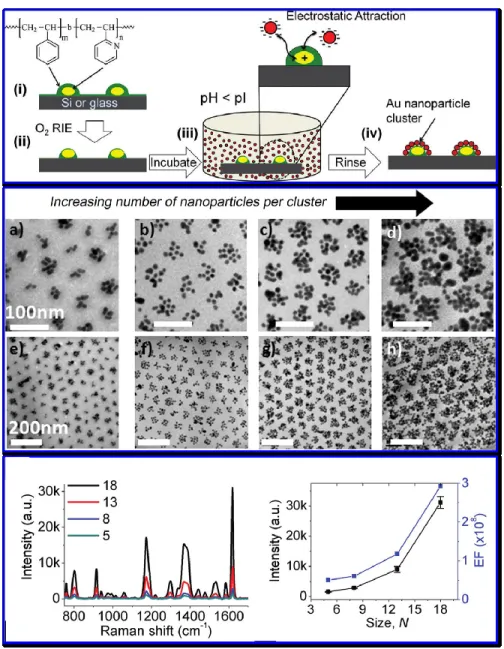
Figure. 1.6 summarizes a collection of nanosized objects that have been employed as platforms for constructing SERS nanopipettes. Glass nanopipettes are a convenient platform for fabricating SERS nanopipettes. They are produced by a laser-based heating and pulling process from glass rods or capillaries of millimeter thickness as well as from optical fibers. They enable the interfacing between a nanostructure and a macroscopic handle and have been used as cellular probes for decades.30 However, the rigid structure of glass nanopipettes renders them easy to buckle when penetrating a cell. Carbon nanopipettes were therefore developed by Bau and coworkers by using glass pipettes as templates.31-34 Carbon nanopipettes showed good mechanical and electrical properties in single cell sensing experiments.31-32,34-35 However, the size of carbon-coated glass nanopipettes is relatively large and their conical shape often causes cell damage. Many researchers have instead employed carbon nanotubes, which can be attached on a glass nanopipette.25,28,36 Metal nanowires can similarly be attached to a glass nanopipette.19
Because metal nanowires are themselves plasmonic nanostructures, no further decoration of nanoparticles is needed in order to make it SERS-active.19 AFM tips have also been shown to be suitable nanoprobes37 for cellular studies or for attaching carbon nanotubes.36
Figure 1.6. Various nanoprobes that have been used as platforms for SERS sensing: A, a
glass nanopipette coated with gold nanoparticles. Reproduced with permission from Ref. 23. Copyright (2009), American Chemical Society. B, a gold nanoparticles-coated carbon nanotube attached to a glass nanopipette. Reproduced with permission from Ref. 25. Copyright (2011), Nature Publishing Group. C, a silver nanowire attached to a glass nanopipette. Reproduced with permission from Ref. 19. Copyright (201), John Wiley & Sons. D, a single silver nanorod deposited on a glass nanopipette. Reproduced with permission from Ref. 35. Copyright (2016), American Chemical Society. E, an AFM tip coated with gold nanoparticles. Reproduced with permission from Ref. 36. Copyright (2016), Nature Publishing Group. F, a carbon nanotube coated with quantum dots attached to an AFM tip. Reproduced with permission from Ref. 36. Copyright (2007), United States National Academy of Sciences.
10
1.3.2 Detection using SERS nanoprobes
SERS nanopipettes can probe heterogeneous content at different specific locations inside living cells. For example, by inserting a SERS nanopipette into the nucleus or the cytoplasm of a single living cell, Vitol et al. obtained two distinct SERS spectra with high signal intensities at the two different locations (Figure 1.7a).23 A dynamic behavior was observed over time by the SERS nanopipette, which allowed the authors to measure time-resolved SERS spectra to uncover the cellular response to KCl stimulation.23 The dynamic behavior, plus the high temporal resolution of SERS, was also exploited in the Masson group to monitor the extracellular metabolites of a single Madin-Darby canine kidney (MDCKII) epithelial cell.20 The SERS nanopipette demonstrated the capability of simultaneous detection of multiple metabolites, such as pyruvate, lactate, ATP, and urea, through a bar-coding data analysis process, and the potential for mapping the concentration gradient of the metabolites near cells was demonstrated (Figure 1.7b).20 Because SERS nanopipettes could only detect molecules that are close to the surface of nanoparticles, the above-mentioned examples rely on weak and nonspecific interactions between molecules and nanoparticles. However, immunoassay capability can be imparted to the SERS nanopipette for the specific capture and detection of targeted molecules.21 Using the SERS immunoassay sketched in Figure 1.7c, Masson et al. have demonstrated the specific detection of IgG by the SERS nanopipette (Figure 1.7d).21 Such a configuration also benefited from using Raman reporter molecules with their strong and distinct Raman bands as well as from using secondary nanoparticles to further enhance SERS signals.21 According to some researchers, the future of nanopipette technology is lab-on-a-tip, where a nanopipette can perform several tasks at the same time. Singhal et al. reported a multifunctional SERS nanopiette based on carbon nanotubes.25 In addition to SERS sensing, the electrical conduction of carbon nanotubes allows simultaneous electrophysiological measurements (Figure 1.7e and f) and the hollow nanotube provides channels for fluid transport.
Figure 1.7. a, SERS spectra from the cell nucleus (upper spectrum), cytoplasm (middle
spectrum) obtained with the SERS nanopipette, and the blank before insertion. Reproduced with permission from Ref. 23. Copyright (2009), American Chemical Society. b and c, Schematic illustration of the immunoassay on a SERS nanopipette and SERS spectra collected from SERS-nanopipettes in the presence (red) and absence (black) of 1.1 µM IgG. Reproduced with permission from Ref. 21. Copyright (2014), American Chemical Society. d, Plot of relative number of events for lactate and pyruvate near MDCKII cells as a function of nanosensor-cell distance. Reproduced with permission from Ref. 20. Copyright (2016), American Chemical Society. e and f, Simultaneous SERS and electrochemical detection on a SERS nanopipette. Reproduced with permission from Ref. 25. Copyright (2011), Nature Publishing Group.
1.3.3 Fabrication of SERS nanoprobes
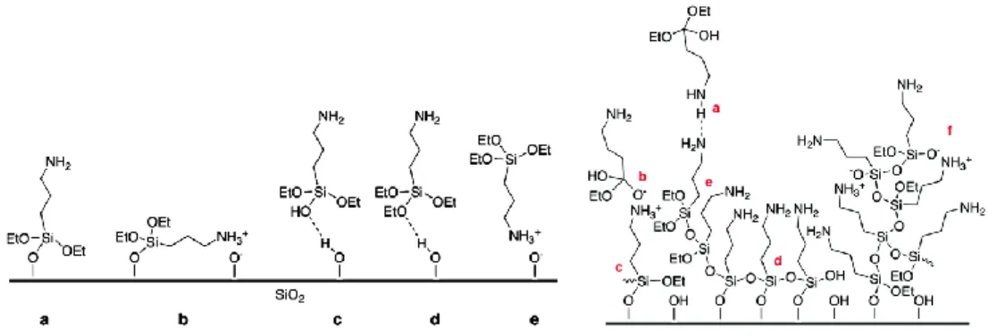
1.3.3.1 Aminosilane self-assembled monolayers
As with other SERS substrates, to render the nanoprobes SERS active, it is necessary to coat them with plasmonic nanoparticles. The immobilization is often accomplished through surface modification with functional groups that provide attractive
12
interactions to nanoparticles. Aminosilane self-assembled monolayers (SAMs) are the most commonly used templates for incorporating nanoparticles to glass and silicon surfaces.38-42 These bifunctional small molecules can covalently attach to SiO2 surfaces through silanol bonds with their amine endgroups to attract nanoparticles via electrostatic interactions. Besides silanol bonds, various other interactions, such as hydrogen bonding and electrostatic interactions, exist between aminosilane molecules and the substrate and among aminosilane molecules themselves (Figure 1.8).43-44 As a result, aminosilane SAMs are multiple layered in nature and often contain loosely attached molecules. In addition, the silanization process is affected by ambient humidity and silane purity, resulting in the formation of oligomers and polymers, which can also react with and attach to the surface.43 These issues associated with SAMs often lead to irregularities in the AuNPs deposited on them, such as incomplete AuNP coverage and surface AuNP aggregates.20-21
Figure 1.8. Left, different types of interactions between aminosilane molecules and silicon
dioxide substrates: (a) a covalently attached aminosilane molecule with its amine group extending away from the interface, (b) the amine group lying on the surface, and (c-e) weakly bonded aminosilane molecules. Right, an aminosilane-derived layer with structural irregularities: individual silane molecules can be incorporated into the layer via (a) hydrogen bonding, (b) electrostatic attraction, (c) covalent bonding, and (d) horizonatal and (e) vertical polymerization with neighbouring silanes; (f) is oligomeric/polymeric silanes attached to the surface. Reproduced with permission from Ref. 44. Copyright (2008), American Chemical Society.
1.3.3.2 Homopolymer templates
Homopolymer films have also been widely used as templates for the deposition of nanoparticles.45-62 A major advantage in using polymer films is that there are many ways to prepare a homopolymer film on a surface, from simple physical processes such as dip-coating,45,62 spin-coating,45 and adsorption23,49 to chemically bonded coating methods such as end-grafting polymer brushes.53,57-58 Owing to the high molecular weight of polymers, it is easy to obtain uniform and high coverage films. The electrostatic self-assembly deposition of nanoparticles on polymer films is enabled by functional groups contained in polymer chains. For example, the pyridine groups in poly(vinylpyridine) polymer chains can be protonated to carry positive charges to attract negatively charged nanoparticles59 and poly(acrylic acid) can carry negative charges under proper pH for positively charged nanoparticles.59 However, nanoparticles deposited on polymer films typically suffer from different degrees of aggregations.45-49,53,57-58,60,63 The electrostatic repulsion among nanoparticles tend to prevent nanoparticles from aggregating on the surface. However, this stabilization force is weakened as the substrate dries.45 On the other hand, polymer films that are capable of attracting charged or metallic nanoparticles necessarily contain many polar groups and are, thus, swollen by, or gain a certain mobility in, aqueous colloidal solutions of these NPs.45,53,62-63 These combined effects results in the formation of nanoparticle aggregates during the drying of the film.
1.3.3.3 Block copolymer templates
Block copolymer (BCP) thin films can be used to produce highly ordered nanostructures, making them one of the best templates for preparing high-quality SERS chips.10,64-67 Unlike other film templates introduced above, block copolymer thin films generally show nanopatterns on the film surface due to the block immiscibility leading to a self-assembly phenomenon, as will be described in greater detail in the next section. Using appropriate blocks, these nanopatterns can selectively attract gold nanoparticles and thus the patterns in BCP thin films can be used as scaffolds for the controlled deposition or synthesis of surface NP arrays.68-70 The high pattern regularity over large areas, high NP density and tunable center-to-center distances on the nanoscale enabled by BCP templates are particularly beneficial for SERS substrates. Therefore, a variety of techniques have been
14
developed to use self-assembled BCP thin films to produce ordered deposition of nanoparticles,71-76 as will also be described in the following section. However, so far, most BCP templated SERS substrates have been reported on planar substrates71-72,77-78 or sometimes curved substrates with low curvature.79-80 We will explore these templates on highly curved glass nanofibers, in order to make SERS endoscopic probes.
1.4 Block copolymer self-assembly
1.4.1 Microphase separation of diblock copolymers
Linear diblock copolymers are the simplest class of block copolymers. They are composed of two chemically distinct, usually immiscible, polymer chains which are covalently bound together at one end.81-86 Some examples of diblock copolymers are polystyrene-b-poly(methylmethacrylate) (PS-b-PMMA; most studied system for nanolithography),87-88 polystyrene-b-poly(4-vinylpyridine) (PS-b-P4VP), most studied system for supramolecular self-assembly and used in this thesis),89-94 polystyrene-b-poly(ethylene oxide) (PS-b-PEO), polystyrene-b-polylactide (PS-b-PLA),95-96 polystyrene-b-polyisoprene (PS-b-PI),97-98 and polystyrene-b-polydimethylsiloxane (PS-b-PDMS, silicon containing block copolymer),99-100 to name but just a few (Figure 1.9).
Figure 1.9. Chemical structures of some common diblock copolymers.
Because of block immiscibility and the covalent connection between blocks that does not allow large-scale phase separation, BCPs are subject to what is termed microphase
separation, resulting in the spontaneous formation of various types of ordered nanostructures.101-102 (The adjective “microphase” is commonly used where nowadays “nanophase” would be used, because at the time of the discovery of the phase behavior of BCPs, micro was considered very small.102) Figure 1.10 shows the theoretical thermodynamic phase diagram for diblock copolymers, which depicts the conditions under which various microphase-separated morphologies are obtained, including body-centered-cubic spheres (S, S'), hexagonally packed cylinders (C, C'), bicontinuous gyroids (G), and lamellae (L), as well as a disordered region where the blocks are miscible.103-106 The characterization of phase equilibria in a BCP melt is determined by two parameters: the block volume fraction ꝭ and the product χN, where χ is the Flory-Huggins segment-segment interaction parameter between two blocks and N is the degree of polymerization. The size of the domain is dictated by N and the morphology is dictated by ꝭ. The lower limit of the microdomain size is set by the condition (for symmetric BCPs) that χN=10.5, below which the BCP blocks will mix, forming a homogeneous or mixed-phase morphology.
Figure 1.10. Self-consistent mean-field theoretical phase diagram of diblock copolymers at
equilibrium in the melt. χN is the segregation parameter and ꝭ is the volume fraction of one block. The equilibrium morphologies depend on ꝭ: CPS and CPS' = closely packed spheres, S and S' = body-centered-cubic spheres, C and C' = hexagonally packed cylinders, G = bicontinuous gyroids, L = lamellae. Reproduced with permission from Ref. 86. Copyright (2016), John Wiley & Sons.
16
1.4.2 Block copolymer thin films
Block copolymer thin films are of particular interest because of the possibility of obtaining two-dimensional patterns with very high registry and regularity, providing suitable templates for surface nanopatterning (Figure 1.11, top).81-85,103,107-114 For example, a pattern of hexagonal dots can be achieved by using sphere-forming BCP thin films or cylinder-forming BCP thin films where the cylinders are aligned vertically relative to the substrate.115 Cylinders lying parallel to the surface and lamellae standing perpendicular to the surface can be used for producing line patterns.116 Owing to the nanoscale dimensions of BCP patterns (typically 10–100 nm), BCP thin films are a promising approach for the nanofabrication of next-generation microelectronics.117-122 Driven by this goal, a great deal of research has been devoted to BCP thin films and their use for achieving nanoparticle arrays or patterns, as summarized by a number of reviews.83-86,103,108-112,114,123-124 There are two basic nanofabrication strategies based on BCP thin film surface patterning, including the transfer of BCP patterns to underlying substrates by using BCP films as masks for nanolithography (Figure 1.11 bottom)125-131 and the position-selective deposition of nanoparticles (NPs) on BCP domains,10,67,132-134 the latter being addressed in detail in the following section.
Figure 1.11. Top, Schematic representation of microphase-separated BCP thin film
patterns. Reproduced with permission from Ref. 86. Copyright (2016), John Wiley & Sons. Bottom, pattern transfer to the underlying substrate by using BCP films as photolithographic masks. Reproduced with permission from Ref. 116. Copyright (2011), American Chemical Society.
1.4.3 Fabrication of NP arrays using BCP film templates
Four different approaches have been used to fabricate NP arrays via BCP thin films, namely direct deposition of NPs on BCP thin films,73 back-filling of NPs,135 on-site synthesis of NPs,76,136 and preloading of NP precursor into BCP micelles.71
1.4.3.1 Guided deposition of NPs on BCP thin films
The first approach involves using BCP thin film surface patterns to guide the ordered deposition of NPs. Its advantage lies in the broad variety of NPs accessible by