HAL Id: hal-02485106
https://hal.archives-ouvertes.fr/hal-02485106
Submitted on 19 Feb 2020HAL is a multi-disciplinary open access archive for the deposit and dissemination of sci-entific research documents, whether they are pub-lished or not. The documents may come from teaching and research institutions in France or abroad, or from public or private research centers.
L’archive ouverte pluridisciplinaire HAL, est destinée au dépôt et à la diffusion de documents scientifiques de niveau recherche, publiés ou non, émanant des établissements d’enseignement et de recherche français ou étrangers, des laboratoires publics ou privés.
Contact resistivity of Al/Ti ohmic contacts on p-type
ion implanted 4H and 6H-SiC
Roberta Nipoti, Francesco Moscatelli, Andrea Scorzoni, Antonella Poggi, Gian
Cardinali, Mihai Lazar, Christophe Raynaud, Dominique Planson,
Marie-Laure Locatelli, Jean-Pierre Chante
To cite this version:
Roberta Nipoti, Francesco Moscatelli, Andrea Scorzoni, Antonella Poggi, Gian Cardinali, et al.. Con-tact resistivity of Al/Ti ohmic conCon-tacts on p-type ion implanted 4H and 6H-SiC. 2002 MRS Fall Meeting, Dec 2002, Boston, United States. �10.1557/PROC-742-K6.2�. �hal-02485106�
Contact resistivity of Al/Ti ohmic contacts on p-type ion implanted 4H- and 6H-SiC.
Roberta Nipoti, Francesco Moscatelli1, Andrea Scorzoni1, Antonella Poggi, Gian Carlo
Cardinali, Mihai Lazar2, Christophe Raynaud2, Dominique Planson2, Marie-Laure Locatelli2 and
Jean-Pierre Chante2
CNR- IMM Sezione di Bologna, via Gobetti 101, 40129 Bologna
1Dipartimento d’Ingegneria Elettronica e dell’Informazione, Università di Perugia, via G.
Duranti 93, 06125 Perugia
2CEGELY (UMR CNRS n°5005), Bât. Leonard de Vinci, INSA de Lyon, 20, Av. A. Einstein,
F-69621, Villeurbanne Cdx France
ABSTRACT
Al-Ti alloys with 72 wt% Al were employed for the realisation of ohmic contacts on 4´1019 cm-3
p-type ion implanted 4H- and 6H-SiC samples. Contact resistivity characterisations by TLM measurements were done at wafer level in the temperature range 28-290°C. Analysis of the TLM measurements took into account current crowding at the metal pads. More than half of the
evaluated contact resistivity reached the minimum value detectable by the used TLM devices, that was slightly higher than 1´10-6 Wcm2. Above this limit value, contact resistivity decreased
for increasing temperature and was spread over a few decades. The maximum contact resistivity at 28°C was 2´10-4 Wcm2, which changed to 5´10-6 Wcm2 at 290°C. The thermal behaviour of
these TLM structures featured thermionic-field emission conduction.
INTRODUCTION
Al-Ti alloys have been subjects of several electrical, chemical and physical investigations aimed at making ohmic contacts on p-type SiC [1]. The alloy with the 70 wt% Al was found to give the more reproducible specific contact resistivity rc after vacuum annealing at 1000°C for 2
min. These rc values ranged from 1.5´10-4 Wcm2 to 9.5´10-6 Wcm2 for doping concentration
ranging from 7´1018 cm-3 to 1.3´1019 cm-3, respectively, independently of the 4H- or 6H-SiC
polytype [2]. Moreover, the lowest rc values were found to be independent of the alloy ratio [2,
3]. These studies featured as grown SiC epilayer, mesa etching, Al-Ti sintered targets of the desired weight ratio and lift off technology to define the metal pattern for the rc evaluation.
The purpose of this work was to transfer the 70 wt% Al recipe [2] to p-type ion implanted 4H- and 6H-SiC specimens. Due to technological constraints some steps were modified. In particular, single element targets were used and the layer thickness ratio was chosen so to obtain the desired Al/Ti weight ratio. The metal patterns were defined by chemical etching. Different gases in the annealing ambient were studied, namely high purity Ar and vacuum.
The Transmission Line Method (TLM) was used to evaluate the rc of these Al-Ti alloyed
contacts. In particular, the resistance measurements on TLM structures were analysed accounting for two-dimensional (2D) and three-dimensional (3D) current flow.
EXPERIMENTAL
<0001> 8° off-axis 4H-SiC and <0001> on-axis 6H-SiC, n-type wafers supplied by CREE were used for this study. Almost box shaped doping profiles were made at the sample surface via
multiple energy Al+ implantation and high temperature thermal annealing. The substrate
temperature during implantation was varied in the range 27-300°C from sample to sample. The implanted wafers were annealed one by one at 1700°C in an inductively heated J.I.P.ELECTM
furnace equipped with a glassy carbon crucible covered by a SiC disk. The annealing gas was high purity Ar at a partial pressure just above the atmospheric one. Secondary Ion Mass Spectrometry showed the as implanted and annealed doping profiles were the same, while Hall effect measurements at room temperature showed hole density values corresponding to a complete electrical activation of the implanted Al. The p-type implanted layers had doping concentration and thickness equal to 4´1019 cm-3 and 1.35 µm for the 6H-SiC wafer,
4.5´1019cm-3 and 0.38 µm for the 4H-SiC one.
<0001> 3.5° off-axis 6H-SiC wafer by CREE with a 2 µm thick 1´1019cm-3 p-type epilayer
on an n-type substrate was also used for comparison.
The TLM metal patterns were realised by the following recipe. The samples were cleaned consecutively in boiling trichlorethylene, acetone and isopropyl alcohol. This degreasing in organic solvent was followed by the next surface cleaning recipe H2SO4:H2O2 (1:1) for 5min,
deionised water for 3min, HF:H2O=1:10 for 60s, deionised water for 3min. At the end of this
cleaning process, the substrates were dried with N2 gas. Before loading in the vacuum chamber
for metal deposition, the samples were dipped in HF: H2O = 1:1 for 30s and dried with N2 gas.
First Ti (80 nm) and then Al (350 nm) were deposited by sputtering. The chosen thicknesses correspond to 72 wt% Al. Photolithography process and subsequent metal etching were employed to define the metal patterns. Post deposition annealing was done at 1000°C for 2 min and different annealing ambients were tested: high purity Ar gas and vacuum (10-6 torr).
TLM structures featured two mask levels in the case of the implanted wafers and one mask level in the case of the epilayer specimen. In fact, in the former case doped strips, below the metal pads, were defined by mesa etching or selective ion implantation, while in the epilayer case the conductive paths were not confined. In the implanted specimens Van der Pauw (VdP) devices, for a direct extraction of the sheet resistance Rsh of the implanted layers, were defined too. Different sets of TLM devices were used. On the 6H-SiC wafer, 341 µm wide doped strips with 296 µm wide and 132 µm long metal pads with increasing distances between consecutive pads of 18-27-37-57-108 µm were realised (TLM1). On the 4H-SiC wafer, the TLM structures were 150 µm wide doped strips with 94 µm wide and 94 µm long metal contacts with increasing distances between consecutive pads of 9-18.5-28-37.5-47-57 µm (TLM2). While on the epilayer, TLM metal patterns equal to those used for the 4H-SiC specimen were produced. The given figures were measured after contact alloying and by using an optical microscope, with measurement error equal to ± 0.5 µm.
Current-voltage (I-V) measurements on the TLM and VdP devices were performed as a function of the temperature in the range 28-290°C using a computer controlled parametric characterisation system. This was equipped with a Micromanipulator MM6620 semiautomatic probe station, a Temptronic TP315B hot chuck, a Keithley K707 switching matrix (equipped with 7072 and 7174 semiconductor cards) and a Keithley K90 I-V measuring system, composed by a Keithley K2361 synchronisation controller and four Keithley K238 source measure units. An average of ten TLM and ten VdP devices homogeneously distributed over a 35 mm or 50 mm wafers were typically measured per sample type.
rc was evaluated by resistance measurements on TLM structures. These TLM structures
were included in masks designed for the realisation of given SiC devices and it was found their geometry with respect to the sheet resistance of the implanted layers could not be treated by the
usual one-dimensional (1D) approach. Neither the measurements of non-confined TLM structures could be treated by a 1D approach. Thus, lateral current crowding at the metal pads was taken into account under a 2D approximation. As shown in ref. [4-6] this can be done under the assumptions that the sheet resistance of the doped layer between and that below the pads are equal, and that the transfer length is at least three times, or more, the doped strip depth. Taking into account the transfer length is rc dependent the check of the latter condition
was done once the 2D simulated rc was obtained. Should not this condition be fulfilled, a
correction factor for rc would be computed following the indication given in ref. [7].
The sheet resistance of the strip layer was a variable parameter in the 2D code and at the same time it could be directly measured by means of VdP devices. The comparison between these computed and measured values was used as reliability check for the code outputs.
RESULTS
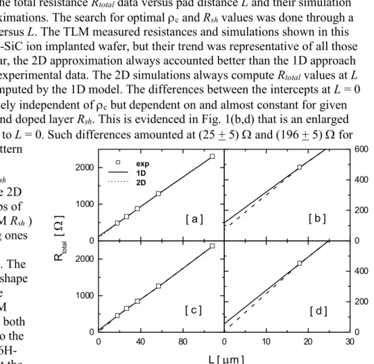
Fig. 1(a,c) shows the total resistance Rtotal data versus pad distance L and their simulation under 1D and 2D approximations. The search for optimal rc and Rsh values was done through a 2D best fit of the Rtotal versus L. The TLM measured resistances and simulations shown in this picture belong to the 6H-SiC ion implanted wafer, but their trend was representative of all those here studied. In particular, the 2D approximation always accounted better than the 1D approach for the curvature of the experimental data. The 2D simulations always compute Rtotal values at L = 0 lower than those computed by the 1D model. The differences between the intercepts at L = 0 were always approximately independent of rc but dependent on and almost constant for given
TLM device geometry and doped layer Rsh. This is evidenced in Fig. 1(b,d) that is an enlarged view of Fig. 1(a,c) next to L = 0. Such differences amounted at (25 + 5) W and (196 + 5) W for the TLM1 and TLM2 pattern
type, respectively. Fig. 2 shows the Rsh values extracted from the 2D model for the doped strips of the TLM structures (TLM Rsh ) versus the corresponding ones obtained from the VdP
measurements (VdP Rsh). The VdP devices had square shape with a side parallel to the wafer flat, while the TLM doped strip were aligned both parallel and orthogonal to the wafer flat. The 4H- and 6H-SiC implanted samples at the minimum and maximum measurement temperatures were chosen as representative of all the samples here studied. The evident spread of the
Figure 1. Two meaningful cases from the 6H-SiC ion
implanted wafer have been chosen to show the trend of the experimental (exp) and simulated (1D, 2D) data. [a] and [c] show the whole measurement range, [b] and [d] are enlarged views close to L = 0. sh c/R r 0 1000 2000 exp 1D 2D [ a ] R to ta l [ W ] 0 200 400 600 [ b ] 0 40 80 0 1000 2000 [ c ] 0 10 20 300 200 400 [ d ] L [ µm ]
VdP Rsh values for each measurement temperature is a consequence of the temperature gradient across the wafer diameter during the ion implantation annealing process as discussed in ref. [8]. Simulated and measured values are linearly related through a factor equal to (1.06 + 0.01).
Taking into account the rc evaluated by the 2D model
and the corresponding transfer length with respect to the thickness of the doped layer, the 2D rc values had to be
transformed into the equivalent 3D ones by applying correction factors in the range 1.2 and 3 [7]. Generally, lower were the 2D rc values higher were the correction
factors. Moreover, it was found that the used TLM geometry did not allow us to extract rc values lower
than approximately 1´10-6 Wcm2.
Figure 2. Sheet resistances of the
TLM structures extracted from the 2D model versus the corresponding values obtained from the VdP measurements. The equivalent 3D rc values are plotted in Fig. 3 versus measurement temperature. Fig.
3(a,b) shows the rc for the not confined TLM devices, i.e. for the 1´1019 cm-3 6H-SiC epilayer.
Fig. 3(a) corresponds to high purity Ar annealing ambient, while Fig. 3(b) to vacuum ambient. The rc values for the ion implanted 4H-SiC and 6H- SiC specimens, i.e. 4´1019 cm-3 doping
density, are shown in Fig. 3(c) and Fig. 3(d), respectively. All the rc values below the minimum
resolution of the method were set equal to 1´10-7 Wcm2. These last rc values were not
meaningful but indicated a very good ohmic performance. The error bars are shown only for one data set per picture and account for the minimisation process between simulated and experimental results.
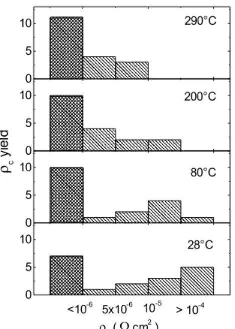
Finally, the yield of the rc values shown in Fig. 3(c,d) is plotted in Fig. 4 for different
measurement temperatures.
DISCUSSION
The linearity of the Fig. 2 plot is an indirect proof of the reliability of the results provided by the simulation code, i.e. of the estimated rcvalues. The fact the proportionality factor differs
Figure 3. Contact resistivity versus
temperature for the not confined TLM patterns alloyed in Ar [a] or vacuum ambient [b], and for the confined TLM devices of the ion implanted 4H-SiC [c] and 6H-SiC [d] wafers. All the evaluated rc
data are shown, while the error bars corresponding to the minimisation procedure between simulated and measured TLM measurements values are shown for only one data set in each sub-figure.
1 10 1 10 slope = 1.06 + 0.01 27 290 °C 4H 6H T LM R sh [ k W / ] VdP Rsh [ kW / ] 0 150 300 10-7 10-6 1x10⁻⁵ 1x10⁻⁴ 10-3 [ a ] rc ( W c m 2 ) 0 150 300 [ b ] Temperature (°C) 0 150 300 [ c ] 0 150 300 [ d ]
1015 1017 1019 10-7 1x10⁻⁵ 10-3 10-1 r c ( W cm 2 ) Doping ( cm-3 ) , 70 wt% Al Crofton 28°C 290°C 6H 28°C 290°C 4H
Figure 5. Contact resistivity versus p-type
doping: comparison between literature (stars) and this work data at room temperature (open square and dots) and 290°C (full square and dots). The literature data referring to the 70 wt% Al are evidenced as full stars.
Figure 4. Yield of the ohmic
contact process for the implanted wafers with respect to the
contact resistivity mapped at wafer level. 4H- and 6H-SiC results were joined.
from 1 within the errors may be due to almost unavoidable non-ideal effects in the VdP geometry and/or a consequence of the approximations used for the 2D simulation of the resistance measurements of the TLM structures. In such a case the correction factors applied to the 2D rc might be different
than the applied ones. Nevertheless it can be remarked that these correction factors were so low that the corrected rc
remained of the same order of magnitude and had the same trend versus temperature as the 2D rc.
A typical problem of the Al/Ti alloyed contact annealed in Ar is the oxidation of the pad top surface [9]. Such an oxide is hard to remove and makes difficult the wafer level
characterisation of the devices. Therefore, post annealing in vacuum is generally preferred. The results plotted in Fig. 3(a) and in Fig. 3(b), show that, once the probing problem was solved, the rcperformances for annealing in high purity Ar or
in vacuum are equivalent. In the light of this result, the rc
values of all the samples here presented were analysed independently of the annealing ambient, as done in Fig.4.
The comparison between Fig. 3(a,b) and Fig. 3(c,d) evidences the spread of the rc values is negligible in the case
of the epitaxial wafer, while it is as large as a few decades for the ion implanted specimens. Such a difference might be attributed to local differences in the electrical activation of the implanted doping species [8]. In fact, when the estimated rc values above the minimum resolution of the method are compared
with the literature data [1-3] the plot of Fig. 5 is obtained. Looking at this figure, we can remark the data of the implanted specimens fall in a region where rc is expected to be high sensitive to
small variation of the doping concentration. A further remark can be done about Fig. 5. The rc evaluated at the highest
temperature has a better agreement with the trend of the published values for contacts with an equivalent weight percent of Al. It looks like the barrier height for conduction was higher in the ion implanted samples than in the epitaxial ones. In general, the thermal behaviour of these rc featured
thermionic-field emission conduction at the contact interface. Nevertheless, even at room temperature, many rc values were
below the minimum detectable limit (see Fig.4), i.e. they were better than the published values. In this case we might speculate about reasons to justify a lower barrier height for conduction in the implanted specimens with respect to the
0 5 10 rc yi el d > 10-4 10-5 5x10⁻⁶ <10-6 rc ( W cm2 ) 28°C 0 5 10 80°C 0 5 10 200°C 0 5 10 290°C
epitaxial substrates. We think such non-homogeneous behaviour of the contacts at wafer level might be understood looking for correlation among electrical performances of different devices at different temperatures. This work is in progress.
Finally, the yields shown in Fig. 4 suggest the technology for the realisation of ohmic contacts to SiC is so mature that the Kelvin resistor method [4] could be introduced for the evaluation of rc on ion implanted SiC, both 4H and 6H.
CONCLUSION
This work demonstrates the technology of Al/Ti alloyed contacts on p-type ion implanted 4H- or 6H-SiC can give quite low values of rc. In fact, in spite of the large spread of the results,
the rcvalues were always lower than 2´10-4 Wcm2 for a medium/high doping concentration of
the implanted layers, i.e. 4´1019 cm-3. Moreover, a non-negligible yield of values below 1´10-6
Wcm2 was found. The results for 4H- and 6H-SiC were similar.
Moreover, this study demonstrates the analysis of non-ideal TLM test structures can be faced and solved by taking into account current crowding, thus reaching a better knowledge about the contact performance.
Work partially funded by the Italian Contracts CNR-MADESS-II and ASI/CNR(1/R/073/01). The clean room staff of CNR-IMM Sezione di Bologna is acknowledged for TLM metal pattern realisation.
REFERENCES
1. J. Crofton, L. Beyer, J. R. Williams, E. D. Luckowski, S. E. Mohney, J. M. DeLucca, “Titanium and aluminum-titanium ohmic contacts to p-type SiC,” Solid-State Electron., 41 , 1725 (1997).
2. J. Crofton, S. E. Mohney, J. R. Williams, T. Isaacs-Smith, “Finding the optimum Al-Ti alloy composition for use as an ohmic contact to p-type SiC,” Solid-State Electron, 46, 109 (2002). 3. J. Crofton, P. A. Barnes, J. R. Williams, J. Edmond, “Contact resistance measurements on
p-type 6H-SiC,” Appl. Phys. Lett., 62 , 384 (1993).
4. A. Scorzoni and M. Finetti, “Metal /semiconductor contact resistivity and its determination from contact resistance measurements”, Material Science Report, 3 no. 2 (1988).
5. Scorzoni, M. Finetti, G. Soncini and I. Suni, “Ohmic contact resistance evaluation in silicon planar structures: application to the CoSi2/n+ interface,” Alta Freq 61, 341 (1987).
6. Finetti, A. Scorzoni and G. Soncini ,“Lateral current crowding effects on contact resistance Measurements in four terminal resistor test patterns,” , IEEE Electron Device Letters,
EDL-5, no. 12, 524 (1984).
7. B. Schuldt, “An exact derivation of contact resistance to planar devices”, Solid-State
Electronics, 21, 715 (1978).
8. M. Lazar, C. Raynaud, D. Planson, M.L. Locatelli, K. Isoird, L.Ottaviani, J.P. Chante, R. Nipoti, A. Poggi, G. Cardinali, “A comparative study of high-temperature aluminium post-implantation annealing in 6H- and 4H-SiC, non uniform temperature effects”, Material
Science Forum 389-393, 827 (2002).
9. F. Moscatelli, A. Scorzoni, A. Poggi, G. C. Cardinali and R. Nipoti “Al/Ti Ohmic Contacts to p-type Ion Implanted 6H-SiC: Mono- and Two-dimensional Analysis of the TLM Data” Accepted for publication in Material Science Forum 2003