HAL Id: hal-00468107
https://hal.univ-brest.fr/hal-00468107
Submitted on 30 Mar 2010HAL is a multi-disciplinary open access archive for the deposit and dissemination of sci-entific research documents, whether they are pub-lished or not. The documents may come from teaching and research institutions in France or abroad, or from public or private research centers.
L’archive ouverte pluridisciplinaire HAL, est destinée au dépôt et à la diffusion de documents scientifiques de niveau recherche, publiés ou non, émanant des établissements d’enseignement et de recherche français ou étrangers, des laboratoires publics ou privés.
Negative group delay active topologies respectively
dedicated to microwave frequencies and baseband signals
Blaise Ravelo, André Pérennec, Marc Le Roy
To cite this version:
Blaise Ravelo, André Pérennec, Marc Le Roy. Negative group delay active topologies respectively dedicated to microwave frequencies and baseband signals. Proceedings of the European Microwave Association, 2008, 4 (2), pp.124-130. �hal-00468107�
Negative group delay active topologies respectively dedicated
to microwave frequencies and baseband signals
Blaise Ravelo, André Pérennec, Marc Le Roy
Abstract – This paper proposes and describes in details the
synthesis, design and implementation of two different active topologies exhibiting negative group delay (NGD) in differ-ent frequency bands. With the first of them, gain and NGD in microwave frequency band are simultaneously achieved; the basic cell consists in a field effect transistor (FET) cas-caded with a shunt RLC series network. The second topol-ogy brings also gain and NGD but is particularly dedicated to baseband signals; this circuit is also built with a FET; but this time in feedback with an RL series network. For both approaches, analytical formulas demonstrating the existence of gain and NGD are proposed together with details about the associated equations, at first for a single cell and then for multi-stage circuits. After implementation of each topol-ogy in a two-stage configuration, the results from experi-ments in frequency-domain are carefully compared to those from simulations; the same thing is done in time-domain for the baseband-dedicated device. Time-domain simulations and measurements highlight the high capability of both to-pologies to compensate or control various dispersive effects. Indeed for both circuits, in case of Gaussianpulse or -modulated signal, the maximum of the output signal exhib-its a time advance compared to the input one of respectively more than 40% and 60% of the standard deviation of the input signal. Moreover, this high relative time-advance is obtained with gain and a pulse compression phenomenon.
Index terms – Active circuits, negative group delay (NGD),
time-domain, baseband signals, pulse compression.
I. Introduction
Artificially constructed materials with simultaneously negative permittivity and permeability, also called “left-handed metamaterials” (LHM), have generated a growing interest in the scientific community. Among their properties not found in nature, the negative re-fractive index, the negative group velocity (NGV) and superluminal group velocity (faster than the speed of light in vacuum c) that occur in LHM, have been par-ticularly studied, discussed and experimentally ob-served in many configurations [1]-[5]. Of course, these abnormal velocities do not violate the require-ments of relativistic causality. In the case of artificial lines with resonant cells that exhibit NGV in narrow frequency band [5], the output signal envelop is fully inscribed with the input one and the pulse advance can be explained through pulse reshaping. In region of anomalous dispersion, NGV is always associated with high transmission losses and is mainly narrowband.
Over the same time period, many authors [6]-[8] have, in parallel, proposed electronic circuits able to pro-duce negative group delay (NGD) and mainly aimed at facilitating the observation of this phenomenon with classical test instruments contrarily to optical or quan-tum experiments [9]-[10]. These circuits being built with operational amplifier and localised components are, thus, restricted to low frequency because of the component bandwidth. They can produce both NGD and amplification for baseband signal up to a few kHz. Group velocity and group delay are related by the length of the device. Then, considering group de-lay is more convenient in the case of a circuit based on lumped components where the length is negligible compared to the wavelength. The group delay defines the time delay applied by the device on the wave packet envelop (or pulse for baseband signals).
The lack of devices with such characteristics, i.e. NGD and gain, in the domain of microwave frequen-cies, has led us to propose in [11]-[12] a new topology of NGD active circuit composed of a resonant RLC series network in cascade with a FET. We fully de-scribe in this paper, the conditions to satisfy NGD, gain and active device requirements, the synthesis equations to design a single cell, and then a multi-stage circuit. With this topology, and contrarily to previous studies with passive or active implementa-tions, NGD, gain and stability can be achieved over broad bands in the microwave domain. For a two-stage circuit, frequency simulations and measurements are compared, and used to generate time-domain simulations. In spite of promising abilities, this topol-ogy is intrinsically unable to provide NGD at very low frequencies. So, we propose here a new topology con-sisting in a FET feedbacked by an RL series network. This topology is used to produce gain and NGD from DC to hundreds of MHz and is then particularly de-voted to baseband signals. An analytical investigation
Received september 30, 2007. Revised 2007.
Laboratoire d’Electronique et Systèmes de Télécommuni-cation (LEST), Unité Mixte de Recherche CNRS (LEST – UMR CNRS 6165), UBO-Telecom Bretagne, 6 avenue Le Gorgeu, CS93837, 29238 Brest cedex 3, France.
Negative group delay active topologies dedicated to microwave and baseband frequencies
Proceedings of the European Microwave Association
2
of these circuit characteristics is proposed and condi-tions to achieve our objectives are also extracted. Fre-quency- and time-domain experimental results are compared to simulations to validate our approach. Fi-nally, conclusions are drawn concerning potential ap-plications and limitations for each topology.
II. Microwave NGD active topology
As stated in the previous section, the group delay, τg,
is the temporal shift of the wave packet through a de-vice of length, L; and this group delay is related to the group velocity, vg, by:
(1) g g
v
L
L
d
dk
d
)
kL
(
d
=
=
=
ω
ω
τ
where k is the ω-dependent wave number. In the case of lumped-element circuit, where L is undefined or negligible compared to the wavelength, it is worth us-ing the concept of group delay instead of group veloc-ity. Indeed, when the scattering parameters are used, as done here, the group delay, τg, is given by:
(2)
ω
ω
φ
τ
d
)
(
d
g=
−
where φ is the frequency-dependent transmission phase.
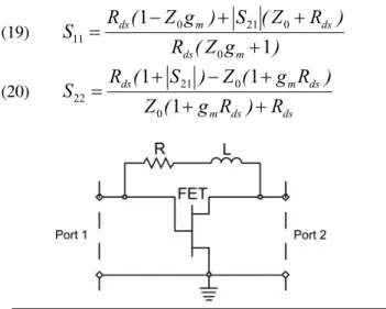
As, all the circuits or lines able to produce NGD at microwave frequencies were affected by high losses, our proposal was to start our study on NGD active cir-cuit with a FET. The target topology had to meet the criteria of compromise between gain and NGD, stabil-ity, output/input matching while being rather simple. At first, to get analytical expressions, we modelled the FET by a voltage-controlled current source of trans-conductance, gm, in cascade with the drain-source
re-sistor, Rds (Figure1).
A) Synthesis equations for a single NGD active cell
The presented NGD active topology devoted to mi-crowave signals is based on a FET cascaded with a shunt series RLC resonant network as depicted in
Fig-ure 2. At the resonance frequency ω0 =1/ LC, and for input and output reference ports normalized to Z0 (50 Ω in practice), the transmission and output reflec-tion parameters are defined as:
(3)
)
R
R
(
Z
R
R
R
g
RZ
)
(
S
ds ds ds m+
+
−
=
0 0 0 212
ω
(4))
R
R
(
Z
R
R
)
R
R
(
Z
R
R
)
(
S
ds ds ds ds+
+
+
−
=
0 0 0 22ω
At ω0, S21 is minimum, but for any judicious values of
R, its modulus can be greater than one and the output
matching satisfied (less than -10 dB). Obtained from eq. (2), where φ is the phase of the S21 parameter, the following expression (5) explicitly shows that the group delay is always negative:
(5)
[
RR
Z
(
R
R
)
]
R
R
LZ
)
(
ds ds ds+
+
−
=
0 0 02
ω
τ
To get a significant NGD value, R must be small, but this is at the expense of the gain value. A satisfying compromise between gain and NGD is reached by set-ting L at a quite high value L and choosing a FET with high Rds and gm values.
For a given transistor, synthesis equations are ex-tracted from relations (3) to (5) in order to calculate the passive element values. These equations are given at the resonance frequency, ω0, and depend on the modulus of the transmission parameter,
) ( 0
21 21 S ω
S = , the output return loss, S22 = S22(ω0) and the NGD level, τ=τ(ω0):
(6) 21 0 0 0 21
2
g
Z
R
(
R
Z
)
S
Z
R
S
R
ds ds m ds+
−
=
(7)[
]
2 21 0 0 2 0 212
g
R
Z
(
R
Z
)
S
)
Z
R
(
g
S
L
ds ds m ds m+
−
−
=
τ
and C is simply deduced from the resonance fre-quency:
Fig. 2. First NGD active topology: FET in cascade with a
shunt series resonant RLC network.
(8) 2 0
1
ω
L
C
=
It comes that the maximum reachable gain for this cell is defined in modulus by:
(9) ds ds m max
Z
R
R
Z
g
)
(
S
+
=
0 0 0 212
ω
One should note that this topology is that of a resistive amplifier, excepted for the components’ values; in-deed, contrary to resistive amplifier, the operating fre-quency is that of the resonant circuit.
B) Design, simulation and experimental results of a two-stage microwave NGD active circuit
As we used in a first time a simplified FET modelling, we built in microstrip technology a two stage circuit aimed to operate at about 1 GHz to validate this ap-proach. A schematic of an n-stage device is proposed in Figure 3. The input of the unit cell presented in Figure 2 is, of course, unmatched. So, the input matching of the first stage is ensured by the shunt re-sistor, Rm, calculated as:
(10) 11 11 0
1
1
S
S
Z
R
m−
+
=
where S11 is the modulus of the desired input return loss of the first cell. On condition to consider that the first cell is as illustrated in Figure 3, the first stage resistor,
R1, is then expressed as a function of S11 and S22: (11)
)
R
Z
(
S
)
S
(
R
Z
g
S
R
Z
R
ds ds m ds+
−
+
=
0 21 11 0 21 0 11
Under this condition, the maximum insertion loss is modified as follows: (12) ds ds m max
R
Z
)
S
(
R
Z
g
S
+
+
=
0 11 0 211
For an intermediate cell, k, the synthesis equations remain those previously described in eqs. (6)-(8). But,
for the nth and last cell, eq. (6) is modified and ex-pressed as a function of S22 of the last stage to match the circuit output:
(13) 22 0 0 0 22
1
S
)
Z
R
(
Z
R
Z
R
)
S
(
R
ds ds ds n−
−
+
+
=
In order to get, at least, stability together with an input and output matching better than -10 dB, a NGD lower than -2 ns and loss compensation at least, we set both stages at the same resonance frequency. The first simulations using ADS microwave circuit simulator of
AgilentTM showed that the adjustments to be made
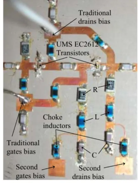
fur-ther to the introduction of connection lines and com-ponent spurious effects were very limited with respect to our first estimates. At last, we carried out an elec-tromagnetic (EM) simulations and a slight optimisa-tion. Traditional gates bias R L C Second gates bias Traditional drains bias Second drains bias UMS EC2612 Transistors Choke inductors
Figure 4 is a picture of the circuit layout with indica-tions about the component characteristics.
0.8 0.9 1.0 1.1 1.2 1.3 1.4 1.5 1.6 0.7 1.7 5 10 15 20 25 30 35 0 40 -5 -4 -3 -2 -1 0 1 -6 2 Simulations Measurements Grou p de lay ( ns ) S ( d B ) 21 (a)
Fig. 4. Photograph of the two-stage active NGD device (28
mm × 22 mm). FET: gm = 98.14 mS and RdS = 116.8 Ω, Rm =
75 Ω, R1 = 11 Ω, R2 = 36 Ω, L1 = L2 = 12 nH, C1 = C2 = 1 pF.
Negative group delay active topologies dedicated to microwave and baseband frequencies
Proceedings of the European Microwave Association
4
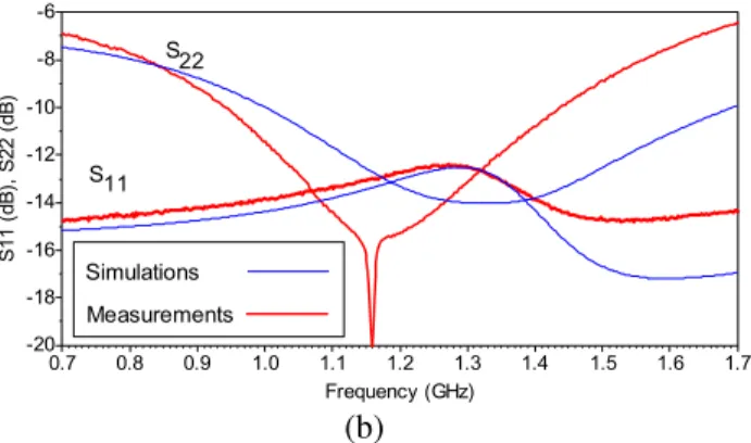
0.8 0.9 1.0 1.1 1.2 1.3 1.4 1.5 1.6 0.7 1.7 -18 -16 -14 -12 -10 -8 -20 -6 Frequency (GHz) S1 1 (d B) , S2 2 ( dB ) Simulations Measurements S22 S11 (b)To investigate for possible simplifications in the de-sign of circuit bias networks, two different biasing paths were tested and gave similar results. In Figure 5, S-parameters and group delay measured by a vector network analyzer show a good agreement with elec-tromagnetic simulation and confirm our expectations. It shows that, around 1 GHz, NGD is -2.3 ns, gain is above 1 dB, input and output return losses are better than -10 dB at the resonance and the overall circuit remains stable over the whole frequency band under measurement (up to 3 GHz). One should, however, note that the total group delay is not exactly the sum of individual cell group delays because of a slight in-ter-stage mismatch. The interest of having a device with NGD and gain is highlighted by time-domain re-sults. tim e (ns) 0 5 1 0 1 5 2 0 2 5 3 0 3 5 in pu t v ol tag e (V ) - 3 .6 0 . 0 1 . 2 - 1 .2 - 2 .4 0 . 6 - 0 .6 - 1 .8 - 3 .0 out put v ol tage (V ) - 1 .2 2 . 4 3 . 6 1 . 2 0 . 0 3 . 0 1 . 8 0 . 6 - 0 .6 (a) 0 .2 time (ns) 0 3 5 output input 1 . 8 4 n s si gn al en ve lo pe s (V ) 0 .4 0 .6 0 .8 1 .0 1 .2 0 .0 5 1 0 1 5 2 0 2 5 3 0 (b)
Those depicted in Figure 6 were extracted from the previous measured scattering parameters with an input signal consisting of a Gaussian pulse modulating a 1.03 GHz carrier The output signal envelop shows an advance of about 46% of the time standard deviation (4 ns) of the input signal. One should note that, thanks to the gain and contrarily to previous studies with NGD microwave passive networks [4]-[5] or with electromagnetic bandgap [13], the output envelop is not fully inscribed in the input one. For the same number of cells as in [5], the time advance is equiva-lent, and the relative advance is higher because of the enlargement of the frequency bandwidth. A wide mi-crowave frequency band with NGD and gain can be synthesised by applying different resonant frequencies to multi-stage circuits [14]. Finally, the main draw-back of this topology is its natural inability to provide NGD at very low frequency, it therefore disqualifies it for baseband applications. Indeed, the following ex-pression of the group delay at very low frequencies (ω tends to zero) is always positive:
(14) 0 0
0
Z
R
R
CZ
)
(
ds ds+
=
τ
As the first topology under study managed to fulfil our initial requirements; we propose a baseband topology around a FET, again.
III. Baseband NGD active topology
We present the basic cell shown in fig 7 made of a FET feedbacked by an RL series network. Again, we use in a first approximation the FET modelling of Figure 1 and look for an interaction between the pas-sive lumped components and the elements of this model.
A) Design equations
So, at a very low frequency (ω tends to zero), the S-parameters of this cell are:
(15)
)
Z
R
(
Z
)
g
Z
Z
R
(
R
)
Z
R
(
Z
)
g
Z
R
(
R
S
m ds m ds 0 0 2 0 0 0 0 2 0 112
+
+
+
+
−
+
−
=
(16))
Z
R
(
Z
)
g
Z
Z
R
(
R
R
Z
S
m ds ds 0 0 2 0 0 0 122
2
+
+
+
+
=
(17))
Z
R
(
Z
)
g
Z
Z
R
(
R
)
R
g
(
R
Z
S
m ds m ds 0 0 2 0 0 0 212
1
2
+
+
+
+
−
=
(18))
Z
R
(
Z
)
g
Z
Z
R
(
R
)
Z
R
(
Z
)
g
Z
R
(
R
S
m ds m ds 0 0 2 0 0 0 0 2 0 222
+
+
+
+
+
−
−
=
Fig. 5. (a) Measured S21 parameter and group delay and (b)
output and input return losses.
Fig. 6. Time responses simulated with the measured
Fig. 8. Input and output return losses (dB(S11), dB(S22))
versus gain (dB(S21)).
From eqs. (15), (17) and (18), the input- and output-return losses can be expressed as a function of the in-sertion loss, |S21| leading to:
(19)
)
g
Z
(
R
)
R
Z
(
S
)
g
Z
(
R
S
m ds ds m ds1
1
0 0 21 0 11+
+
+
−
=
(20) ds ds m ds m dsR
)
R
g
(
Z
)
R
g
(
Z
)
S
(
R
S
+
+
+
−
+
=
1
1
1
0 0 21 22Amplifier stability required a special care. So, for a given transistor, by using eqs. (19)-(20), and according to S21, we define a region where, a priori, input and output matching is gotten. Figure 8 illustrates these conditions (for gm and Rds values of part II-B), where the hatched area is to be avoided.
To alleviate this problem of instability, resistors can be placed in series at the input and output accesses. For the basic cell of Figure 7, the group delay is given by: (21)
[
]
[
( 2 ) ( )]
) 1 ( ) 1 ( ) 1 ( ) 0 ( 0 0 2 0 0 0 0 Z R Z g Z Z R R R g R g Z R L Z g m ds m ds m ds m + + + + − + + + = τwhich becomes negative when: (22)
R
>
1
/
g
mUnder such conditions, the NGD bandwidth goes from DC to the angular cut-off frequency, ω , which is as c
follows: (23)
[
]
)
Z
R
(
R
Z
g
)
(
S
)
(
)
Z
R
(
)
(
S
R
Z
g
ds ds m ds ds m c 0 0 21 2 2 0 21 0 20
0
2
0
2
+
+
−
=
τ
ω
Asω is inversely proportional to c
τ
( 0
)
, it implies touse a multi-stage circuit to get a significant broadband of gain and NGD.
Moreover, the signs of the output and input signals being unlike, the number of stages must be even. This is also true for the first topology under study; it ap-pears as less problematic when the signals are modu-lated. Inversion of eqs. (15) and (20) gives the follow-ing synthesis relations for R and L:
(24)
[
]
) R Z ( ) ( S R g Z ) R g Z R Z ( ) ( S R Z R ds ds m ds m ds ds + − + + + = 0 21 0 0 0 21 0 0 2 2 0 2 (25)[
]
[
]
2 0 0 21 0 0 21 0 2 0 1 1 0 0 2 ds m ds ds m ds m ds m R g Z ) R Z ( ) ( S ) R g ( Z R ) g Z ( ) ( S R g Z ) ( L − + − + + + = τBoth were used to determine the initial values of the cell components. It is worth noting that, for a given FET, a satisfying compromise between gain and NGD can be quickly found by plotting sets of parametric curves. The maximum gain is also given by eq. (9) and depends only on the reference impedance and transistor characteristics (gm, Rds).
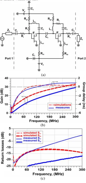
B) Implementation of a two-stage baseband NGD active circuit and frequency- and time-domain measurements
Figure 9 presents the schematic of the device under study, which consists of a two-stage circuit with input and output matching series resistors; it gives also the bias networks and the component values. Combined results of EM simulations of the printed circuit with circuit simulations of the localized components are compared to measurements in Figures 9-b and 9–c. The differences between simulations and measure-ments in Figures 9-a and 9-b are mainly due to ex-trapolation of the transistor S-parameters from the manufacturer datasheet in that frequency band. A sat-isfying agreement is nevertheless obtained for the NGD characteristics. The measured group delay is negative up to more than 100 MHz with simultaneous gain. A wider NGD bandwidth could be produced by applying this method with more stages. But, to easily perform a time domain validation, the number of components was voluntarily limited and the selected
Negative group delay active topologies dedicated to microwave and baseband frequencies
Proceedings of the European Microwave Association
6
Fig. 9. -a) Schematic of the two-stage baseband NGD active
circuit including biasing networks; R1 = R2 = 68Ω, Ri = Ro =
33Ω, L1 = 270nH, Ld1 = Ld2 = 1µH, Rd1 = Rd2 = 68Ω, Rg1 = Rg2 =
1kΩ, C1-7 = 22µF, and F1 = F2 = FET = ATF-55143 (gm= 220
mS, Rds = 230Ω)
-b) gain dB(S21) and group delay
τ
21.-c) input and output return losses (dB(S11) and
dB(S22)).
Fig. 10. Time-domain experimental input and output curves
for the NGD baseband circuit.
frequency band was compatible with test instruments available within our lab.
(a)
(b)
(c)
The measurements were made by using a function generator delivering, in practice, a signal close to a Gaussian pulse (8 ns standard deviation) and a 2Gs/s LeCroy Digital oscilloscope. Input and output circuit accesses were directly connected to the scope through coaxial tee with no cable to avoid spurious reflections or delays. The cumulate delay (approximately 1 ns)
due to the input and output tees has been deembedded from initial measurements prior to the production of Figure 10 in order to place time- and frequency-domain measurements in the same reference planes (as defined by ports 1 and 2 in Figure 9-a).
Finally, for a same ordinate scale, Figure 10 shows that the output pulse maximum has a time advance of more than 60% (more of 5 ns) with respect to the in-put standard deviation with a slight distortion.
IV. Conclusion
We proposed two different ways to generate NGD without losses. The conditions required to get NGD, gain and the design requirements of active device were introduced from analytical relations. Each topol-ogy was scrupulously validated through the measure-ments of corresponding two-stage prototypes. The first topology, thanks to its simplicity, its possibility of achieving broad bandwidth, and loss compensation, could be applied to compensate dispersive effects or in the design of UWB phase shifters by using the area of positive phase slope. However, its intrinsic limita-tion at low frequency led us to investigate another to-pology more dedicated to baseband signals. The pro-totype proposed here meets this requirements and seems particularly well suited to find applications in interconnect delay compensation. Indeed, the group delay proved to be only negative up to a hundred of MHz for measurements convenience, but a wider bandwidth could be achieved by a device with more stages.
Acknowledgment
The authors would like to thank B. Della and P. Coant from Telecom Bretagne and A. Bourrières from IUT of Brest for the different circuits’ implementation.
References
[1] Pendry, J. B.: Negative refraction makes a perfect lens. Phys. Rev. Lett., 35 (2000), 3966-3969.
[2] Shelby, R. A.; Smith, D.R.; Schultz, S.: Experimental verification of a negative index of refraction. Science,
292 (2001), 77-79.
[3] Eleftheriades, G.V.; Iyer, A.K.; Kremer, P.C.: Planar negative refractive index media using periodically L-C loaded transmission lines. IEEE Trans. Microwave Theory Tech., 50 (2002), 2702–2712.
[4] Siddiqui, O. F.; Mojahedi, M.; Eleftheriades, G. V.: Periodically Loaded Transmission Line With Effective Negative Refractive Index and Negative Group Veloc-ity. IEEE Trans. Antennas Propagat., 51(2003), 2619-2625.
[5] Siddiqui, O.F.; Erickson, S.J.; Eleftheriades, G.V.; Mojahedi, M.: Time-domain measurement of negative group delay in negative-refractive-index transmission-line metamaterials. IEEE Trans. Microwave Theory Tech., 52 (2004), 1449-1454.
[6] Solli, D.; Chiao, R.Y.: Superluminal effects and nega-tive delays in electronics, and their applications. Physical Review E, 5 (2002).
[7] Kitano, M.; Nakanishi, T.; Sugiyama, K.: Negative Group Delay and Superluminal Propagation: An Elec-tronic Circuit Approach. IEEE Journal of Selected Topics in Quantum Electronics, 9 (2003), 43-51. [8] Nakanishi, T.; Sugiyama, K.; Kitano, M.:
Demonstra-tion of negative group delays in a simple electronic circuit. American Journal of Physics, 70 (2002), 1117-1121.
[9] Chiao, R.Y.: Atomic coherence effects which produce superluminal (but causal) propagation of wavepackets. Quantum Opt. 6 (1994), 359-369.
[10] Dogariu, A.; Kuzmich, A.; Cao, H.; Wang, L. J.: Su-perluminal light pulse propagation via rephasing in a transparent anomalously dispersive medium. Optics Express, 8 (2001).
[11] Ravelo, B.; Pérennec, A.; Le Roy, M.: Synthèse et ré-alisation de circuits actifs à temps de propagation de groupe negative. 15th JNM, 2007, Toulouse, France.
[12] Ravelo, B.; Pérennec, A.; Le Roy, M.: Active Micro-wave Circuit with Negative Group Delay. IEEE Microw. Wirel. Compon. Lett., 17 (2007), 861–863. [13] Le Roy, M.; Lheurette, E.; Pérennec, A.: Pulse
Com-pression with Superluminal Group Velocity in 1-D Photonic Bandgap Coplanar Waveguide. 34th Euro-pean Microwave Conference, Amsterdam, 11 – 15 Oc-tober 2004, pp. 463 – 466.
[14] Ravelo, B.; Pérennec, A.; Le Roy, M.: Synthesis of broadband Negative Group Delay Active Circuits. Proc. IEEE MTT-Symposium IMS 2007, 2007, Hono-lulu (Hawaii), 2177-2180.
Blaise Ravelo was born in Tananarivo
(Madagascar) in 1978. He received the Research Master 2nd degree in electronics
from the University of Brest (France) in 2005. Currently, he is working toward the Ph. D. Degree in electronics within the Laboratoire d’Electronique et Systèmes
de Télécommunications (LEST-UMR CNRS 6165) at the same university, where he also serves as a Teaching Assistant. His current research interests include left-handed planar circuits and the design of passive and active microwave devices with negative group delay.
André Pérennec was born in Quimper,
France, in 1960. He received the Ph.D degree in electronics from the "Université de Bretagne Occidentale" (France) in 1988. Presently, he is “Maître de con-férences” in the Laboratory for Electronics and Telecommunication Systems (LEST, UMR CNRS 6165), Brest, France. His research interests are in the active and passive device microwave area and include am-plifier design (low-noise and broad-band), and filters. He has also worked on optoelectronic devices. Currently, his main re-search interests concern metamaterials and negative group de-lay circuits.
Marc Le Roy was born in Brest, France,
in 1970. He received the Ph.D. degree in electronics from the LEST (Laboratory for Electronics and Telecommunication Systems, UMR CNRS 6165) at the Uni-versity of Bretagne Occidentale, Brest, France, in 1999. He rejoined the LEST in 2003 as a Maître de conférences. His re-search activities deal with modelization and design of nonuni-form and periodic structures for optical and microwave sys-tems, metamaterials and negative group delay circuits.