HAL Id: hal-00468133
https://hal.univ-brest.fr/hal-00468133
Submitted on 30 Mar 2010
HAL is a multi-disciplinary open access archive for the deposit and dissemination of sci-entific research documents, whether they are pub-lished or not. The documents may come from teaching and research institutions in France or abroad, or from public or private research centers.
L’archive ouverte pluridisciplinaire HAL, est destinée au dépôt et à la diffusion de documents scientifiques de niveau recherche, publiés ou non, émanant des établissements d’enseignement et de recherche français ou étrangers, des laboratoires publics ou privés.
Broadband Balun Using Active Negative Group Delay
Circuit
Blaise Ravelo, André Pérennec, Marc Le Roy
To cite this version:
Blaise Ravelo, André Pérennec, Marc Le Roy. Broadband Balun Using Active Negative Group
Delay Circuit. 37th European Microwave Conference, Oct 2007, Munich, Germany. pp.466-469, �10.1109/EUMC.2007.4405228�. �hal-00468133�
Broadband Balun Using Active Negative Group
Delay Circuit
Blaise Ravelo, André Pérennec, Marc Le Roy
LEST-UMR CNRS 6165 – UBO/ENSTBr – CS93837, F-29238 – 6, Avenue Le Gorgeu, BREST CEDEX 3, FRANCE
[email protected] [email protected]
Abstract—In this paper, a broadband balun using an active
circuit with negative group delay (NGD) is proposed. The unit cell of the active NGD circuit is based on a Field Effect Transistor (FET) in cascade with an RLC series network. First, a comparison between measurements of a two-stage prototype of this active topology and simulations validate the synthesis method of this innovative device. Then, thanks to the NGD circuit, a constant phase can be generated if this circuit is associated with a classical transmission line. By implementing such phase shifters into the two branches of a resistive splitter, we obtain a new balun topology. The NGD balun simulation results show a rather constant differential output phase (180°±9°), insertion losses above -2.4 dB and an excellent isolation below -59 dB for all three ports, for a bandwidth from 3.5 GHz to 5.5 GHz.
I. INTRODUCTION
In the late 1960s, Veselago [1] has proposed the theory of materials exhibiting both negative permittivity and permeability. More than thirty years later, Pendry and Smith [2]-[3] have experimentally validated this theory for 3-D artificial media. Several experimentations [4]-[5] have since proposed and validated the implementation of such materials, also known as metamaterial, in 2-D and 1-D in planar technologies.
Under certain conditions, these materials may exhibit Negative Group Velocity (NGV). This notion directly related to Negative Group Delay NGD), has been widely discussed and particularly in regions of anomalous dispersion by Brillouin and Sommerfeld [6]. Recently, many experimentations and theoretical studies have shown that NGV exists. For example, Wang et al. [7] has verified this property experimentally in optic system with gaussian pulse which presents negative group delay of 3% of the standard deviation. In fact, for a material of length L, the group delay τ and the group velocity vg are linked by the relation τ = L/vg.
This implies that for electronic circuit based on lumped elements, the length L does not have a physical significance. In this context, the group delay is a more versatile notion.
Indeed, two different teams [8]-[9] have obtained NGD with an electronic circuit built with an operational amplifier and a feedback passive circuit which is frequency limited by the component bandwidth. In the microwave domain, Eleftheriades [10] has proposed a passive left-handed resonant circuit producing a high relative NGD values in a narrow bandwidth but with high losses. To design an NGD circuit
suitable for microwave applications, a solution to compensate for such losses must be proposed. Then, in [11], we have described a new topology of active NGD microwave circuit composed of a resonant RLC series network in cascade with a FET.
This paper is devoted to the insertion of this NGD circuit in the design of a resistive balun to achieve broadband characteristics. This balun comprises an 1x2 (3dB) splitter with the association of a transmission line and an active NGD circuit in each branch. In section II, the NGD active topology is described through the design equations of a unit cell, and an experimental validation is carried out for a two-stage circuit. The following section presents the structure of the proposed balun that convert a single input to two output ports having opposite phases over a broad bandwidth. Then, the simulated performances of this NGD balun are discussed.
II. TOPOLOGY OF ACTIVE NGDCIRCUIT
The unit cell of the NGD topology (fig. 1) consists of an RLC series network in cascade with a FET [11].
Fig. 1. Unit cell of active NGD circuit and low frequency model of the FET.
A. Synthesis Method of active NGD circuit
To get easy-to-use analytical expressions, we first model the FET by a voltage controlled current source with a transconductance, gm, in cascade with the drain-source resistor, Rds. Then, the S-parameters of this cell are defined as:
0 , 1 12 11 = S = S , ) ( 2 0 0 0 21 ds ds ds m R Z Z R Z Z R Z g S + + − = , (1)
) ( ) ( 0 0 0 0 22 ds ds ds ds R Z Z R Z R Z Z R Z S + + − + − = , (2) with ( 1 ) ω ω C L j R Z = + − and Z0 = 50 Ω.
From (2) at the angular resonance frequency,
LC
/ 1
0=
ω and following the specified objectives
) ( 0 21
21 S ω
S = and a negative group delay τ =τ(ω0), the
network synthesis equations [11] are established as:
21 0 0 0 21 ) ( 2g Z R R Z S Z R S R ds ds m ds + − = , (3)
[
]
2 21 0 0 2 0 21 ) ( 2 ) ( S Z R Z R g Z R g S L ds ds m ds m + − − = τ , (4)and C is deduced from the resonance frequency:
2 0 1 ω L C= . (5)
Moreover, a resistor, Rm, is placed in parallel to match the
input.
B. Experimental Validation
Using the previous synthesis relations and a final optimization including all the complete modelling, a two-stage circuit have been designed (fig. 2-a).
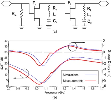
(a) 0.8 0.9 1.0 1.1 1.2 1.3 1.4 1.5 1.6 0.7 1.7 5 10 15 20 25 30 35 0 40 -5 -4 -3 -2 -1 0 1 -6 2 Frequency (GHz) S21 T ( dB) G rou p D elay (n s) Simulations Measurements (b) 0.8 0.9 1.0 1.1 1.2 1.3 1.4 1.5 1.6 0.7 1.7 -18 -16 -14 -12 -10 -8 -20 -6 Frequency (GHz) S1 1T (dB), S22T (d B) Simulations Measurements S22T S11T (c)
Fig. 2-a Schematic of active NGD circuit (Rm = 75 Ω, R1 = 11 Ω, R2 = 36 Ω,
L1 = L2 = 12 nH, C1 = C2 = 1 pF and F1 = F2 = PHEMT-EC2612 (gm = 98.14
mS and Rds = 118.6 Ω), substrate RF35 (εr = 3.5, h = 0.508 mm);
2-b simulated and measured transmission parameter S21 and group delay,
2-c comparison of simulated and measured input and output return losses.
At 1 GHz, (2) gives results really close to those obtained with the more complete model. The good agreement between simulation and measurement results (fig. 2-b and -c) both validates the Negative Group Delay topology and the synthesis equations. Indeed, at 1.07 GHz a -2.3 ns NGD is obtained with input/ouput matching and a gain around 2 dB. A slightly higher NGD bandwidth is achieved than from left-handed resonant approach [10] with the same number of cell. Moreover, to achieve a constant and negative group delay for a wide frequency band, many series RLC networks with different resonance frequencies [12] may be placed in parallel at the same point.
III. PROPOSED BALUN STRUCTURE
The proposed topology of balun with active NGD circuit is depicted in fig. 3 and consists of a power divider Pwd with in cascade in each branch a classical Transmission Line (TL1 and TL2) and a NGD circuit.
Pwd
Fig. 3. Proposed architecture of balun with NGD.
The power divider ensures an equal power split associated with good return losses and isolation. In [13]-[14], Wilkinson dividers are used; then, to get opposite phases at the output of the balun, the first branch exhibits, for a specified frequency, a phase shift of +90° and the second one -90°, instead of -270° and -90° in a conventional balun. Here, we stay in this conventional configuration but, in each branch of the splitter, we associate a transmission line with a negative phase slope and a NGD active circuit with a positive phase slope to finally
achieve a constant phase value over a broadband defined between two frequencies f1 and f2 for both outputs. This
principle is illustrated on fig. 4 for one branch of the proposed balun.
T
rans
mi
ss
io
n ph
as
e
Frequency
NGD
TL
f
2Fig. 4. Illustration of the phase behaviour in each branch.
The fig. 5 shows the schematic of the designed balun with two two-stage active NGD circuits. To keep the broadband, a 6 dB resistive splitter composed by a tree of identical resistors
Z0/3 is used. Then, the transmission lines TLi (i = {1, 2}) are
defined by their length, di, and the characteristic impedance, Zci = Z0. Rm1 and Rm2 allow the matching between the splitter
output and the input access of the branches.
In Fig. 5-a, the top branch (TL1 and NGD1) shows a nearly
flat phase value of -90°(±10°) and for the bottom one (TL2 and NGD2) a -270°(±10°) value from 3 GHz to 6 GHz.
Fig. 4. Schematic of balun with active NGD circuit, Z0 = 50 Ω, R1 = 83 Ω, R2
= 120 Ω, R3 = 22 Ω, R4 = 42 Ω, R5 = 40 Ω, R6 = 43 Ω, R7 = 11.5 Ω, R8 = 36 Ω,
Rm1 = 120 Ω, Rm2 = 150 Ω, L1 = 994 pH, L2 = 315 pH, L3 = 271 pH, L4 = 531
pH, L5 = 3.28 nH, L6 = 6.55 nH, L7 = 1.35 nH, L8 = 3.06 nH, C1 = 2.78 pF, C2
= 2.61 pF, C3 = 2.43 pF, C4 = 2.36 pF, C5 = 0.57 pF, C6 = 0.1 pF, C7 = 0.69 pF,
C8 = 0.63 pF, TL1 (d1 = 4.49 mm, Zc1 = 50Ω), and TL2 (d2 = 24.89 mm, Zc2 =
50 Ω) for substrate RF35 (εr = 3.5, h = 508 µm), FETs are the same as in fig.
2.
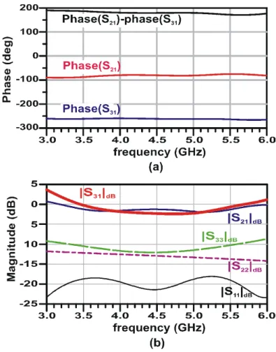
Fig. 5-a and -b show a differential phase output of (180°±9°), insertion losses |S21|dB and |S31|dB of more
than -2.4dB, isolation less than -59 dB for all ports and |S11|dB
and |S22|dB are less than -11dB from 3 GHz to 6 GHz and the
output return loss |S33|dB is below -9dB. Finally, ||S31|dB-|S21|dB|
is less than 1.1dB from 3.5 GHz to 6 GHz.
Fig.5-a. Simulated phases in degrees of S21, S31 and their difference, and -b
simulated return S11(dB), S22(dB) and S33(dB), and insertion losses S21(dB)
and S31(dB).
In table I, the variations through the two branches of the magnitude and phase of S21 and S31 are given from 3.5 GHz to
5.5 GHz.
TABLEI
PHASE AND MAGNITUDE VARIATION FROM 3.5GHZ TO 5.5GHZ
Magnitude (dB) Phase (deg.) Insertion
loss Min. Max. Min. Max.
S21 -1.94 -1.24 -87.47 -79.01 S31 -2.40 -0.24 -263.40 -260.01
For such an active circuit, stability must be ensured for all frequencies. This circuit stability analysis has been made by carefully verifying that the magnitude of the input and output reflexion coefficients of each transistor was kept below one.
IV. CONCLUSIONS
A new balun topology based on active NGD circuit has been presented that exhibits a differential phase output of
180°(±9°) and insertion losses above -2.4dB for a frequency band of 3.5 GHz to 5.5 GHz. Thanks to the FET non-reciprocity, a good isolation of all balun ports is guaranteed. Each branch includes a phase shifter with an absolute flat phase characteristic over a broad bandwidth. This is made possible thanks to a new active topology able to deliver simultaneously gain and negative group delay or positive phase slope over a broad bandwidth. This new topology is defined by synthesis equations which have been already validated thanks to a previous realization. Active NGD circuits are particularly well-suited to be used in UWB phase shifters with constant phase versus frequency. Moreover, implementation of this topology in distributed circuit configuration is possible for higher frequency applications.
REFERENCES
[1] V. Veselago, “The electrodynamics of substances with simultaneously values of ε and µ”, Soviet Physics Uspekhi, vol. 10, no. 4, pp. 509-514, 1968.
[2] J. B. Pendry, “Negative Refraction Make a Perfect Lens”, Phys. Rev.
Lett. 85, 3966, 2000.
[3] R. A. Shelby, D. R. Smith and S. Schultz, “Experimental verification of a negative index of refraction”, Science, vol. 292, no. 5514, pp. 77-79, Ap. 2001.
[4] George V. Eleftheriades, Omar Siddiqui, and Ashwin K. Iyer, “Transmission Line for Negative Index Media and Associated
Implementations Without Excess Resonators”, in IEEE MWC Lett., vol. 13, n° 2, 51, Feb. 2003.
[5] A. Lai, C. Caloz, and Itoh, “Composite Right/Left-Handed transmission Line Metamaterials”, IEEE Microwave Magazine, vol. 5, pp. 34-50, Sep. 2004.
[6] L. Brillouin, and A. Sommerfeld, “Wave Propagation and Group Velocity”, Academic Press, New York, 1960, pp. 113-137.
[7] L. J. Wang, A. Kuzmich and A. Dogariu, “Gain-Assisted Supraluminique Light Propagation”, Nature 406, pp. 277-279, June 2000.
[8] D. Solli, and R. Y. Chiao, “Superluminal effects and Negative delays in Electronics and their Applications”, Physical Review E, Issue 5, Nov. 2002.
[9] M. Kitano, T. Nakanishi, and K. Sugiyama, “Negative Group Delay and Superluminal Propagation : An electronic circuit Approach”, IEEE
Journal of selected Topics in Quantum electronics, vol. 9, no1, pp.
43-51, 2003.
[10] O. Siddiqui, M. Mojahedi, S. Erickson, and G. V. Eleftheriades, “Periodically Loaded Transmission Line with Effective Negative Refractive Index and Negative Group Velocity”, IEEE Transactions on
Antennas and Propagation, vol. 51, no. 10, oct. 2003.
[11] B. Ravelo, A. Pérennec, and M. Le Roy, “Synthesis of broadband Negative Group Delay Active Circuits”, Proceedings of International
Microwave Symposium (IMS2007), Honolulu, Hawaii, 3-8 June 2007.
[12] C. D. Broomfield and J. K. A. Everard “Broadband negative group delay networks for compensation of oscillators using feedforward amplifiers.” Electronics Letters, vol. 20, pp. 1710-1711, Sep. 2000. [13] M. A. Antoniades, and G. V. Eleftheriades, “A BroadBand Wilkinson
Balun Using Microstrip Metamaterial Lines”, IEEE Antennas and
Wireless Propagation Letters, vol. 4, 2005
[14] S. Lee, Jong-Sik Lim, Hoe-Sung Yang and S. Nam, “A Novel Design Of Balun using Left Handed Transmission Line”, Proceedings of