HAL Id: tel-02918008
https://tel.archives-ouvertes.fr/tel-02918008
Submitted on 20 Aug 2020HAL is a multi-disciplinary open access archive for the deposit and dissemination of sci-entific research documents, whether they are pub-lished or not. The documents may come from teaching and research institutions in France or abroad, or from public or private research centers.
L’archive ouverte pluridisciplinaire HAL, est destinée au dépôt et à la diffusion de documents scientifiques de niveau recherche, publiés ou non, émanant des établissements d’enseignement et de recherche français ou étrangers, des laboratoires publics ou privés.
plasma etching processes for advanced memories
application
Maria Mercedes Rizquez Moreno
To cite this version:
Maria Mercedes Rizquez Moreno. Characterization and optimization of high density plasma etching processes for advanced memories application. Other. Université de Lyon, 2016. English. �NNT : 2016LYSEM024�. �tel-02918008�
N°d’ordre NNT : 2016LYSEM024
THESE de DOCTORAT DE L’UNIVERSITE DE LYON
opérée au sein de
L’Ecole des Mines de Saint-Etienne
Ecole Doctorale
N° 488
Sciences, Ingénierie, Santé
Spécialité de doctorat
: Microelectronics/ MicroélectroniqueSoutenue publiquement le 08/11/2016, par :
María Rízquez
Characterization and optimization of high
density plasma etching processes for
advanced memories application
« Caractérisation et optimisation des procédés de gravure plasma haute densité pour application sur des dispositifs de type mémoires électroniques avancées »
Devant le jury composé de:
REIS Marco/ Professeur/ Université Coimbra (Portugal) Présidente LANDESMAN, Jean-Pierre/ Professeur–Directeur/Université Rennes 1 (France) Rapporteur DUSSART, Rémi/Professeur/ Université d’Orleans (France) Rapporteur REIS Marco/ Professeur/ Université Coimbra (Portugal) Examinateur PINATON Jacques/Responsible process control group/ STMicroelectronics Examinateur PASQUET Julien/Responsible plasma etching group/ STMicroelectronics Examinateur ROUSSY Agnès/Maitre-Assistant-HdR/ EMSE CMP-SGC Directrice de thèse
ABSI Nabil CR Génie industriel CMP
AUGUSTO Vincent CR Image, Vision, Signal CIS
AVRIL Stéphane PR2 Mécanique et ingénierie CIS
BADEL Pierre MA(MDC) Mécanique et ingénierie CIS
BALBO Flavien PR2 Informatique FAYOL
BASSEREAU Jean-François PR Sciences et génie des matériaux SMS BATTON-HUBERT Mireille PR2 Sciences et génie de l'environnement FAYOL
BEIGBEDER Michel MA(MDC) Informatique FAYOL
BLAYAC Sylvain MA(MDC) Microélectronique CMP
BOISSIER Olivier PR1 Informatique FAYOL
BONNEFOY Olivier MA(MDC) Génie des Procédés SPIN
BORBELY Andras MR(DR2) Sciences et génie des matériaux SMS
BOUCHER Xavier PR2 Génie Industriel FAYOL
BRODHAG Christian DR Sciences et génie de l'environnement FAYOL
BRUCHON Julien MA(MDC) Mécanique et ingénierie SMS
BURLAT Patrick PR1 Génie Industriel FAYOL
CHRISTIEN Frédéric PR Science et génie des matériaux SMS
DAUZERE-PERES Stéphane PR1 Génie Industriel CMP
DEBAYLE Johan CR Image Vision Signal CIS
DELAFOSSE David PR0 Sciences et génie des matériaux SMS
DELORME Xavier MA(MDC) Génie industriel FAYOL
DESRAYAUD Christophe PR1 Mécanique et ingénierie SMS DJENIZIAN Thierry PR Science et génie des matériaux CMP
DOUCE Sandrine PR2 Sciences de gestion FAYOL
DRAPIER Sylvain PR1 Mécanique et ingénierie SMS
FAVERGEON Loïc CR Génie des Procédés SPIN
FEILLET Dominique PR1 Génie Industriel CMP
FOREST Valérie MA(MDC) Génie des Procédés CIS
FOURNIER Jacques Ingénieur chercheur CEA Microélectronique CMP FRACZKIEWICZ Anna DR Sciences et génie des matériaux SMS
GARCIA Daniel MR(DR2) Génie des Procédés SPIN
GAVET Yann MA(MDC) Image Vision Signal CIS
GERINGER Jean MA(MDC) Sciences et génie des matériaux CIS GOEURIOT Dominique DR Sciences et génie des matériaux SMS GONDRAN Natacha MA(MDC) Sciences et génie de l'environnement FAYOL GRAILLOT Didier DR Sciences et génie de l'environnement SPIN
GROSSEAU Philippe DR Génie des Procédés SPIN
GRUY Frédéric PR1 Génie des Procédés SPIN
GUY Bernard DR Sciences de la Terre SPIN
HAN Woo-Suck MR Mécanique et ingénierie SMS
HERRI Jean Michel PR1 Génie des Procédés SPIN
KERMOUCHE Guillaume PR2 Mécanique et Ingénierie SMS KLOCKER Helmut DR Sciences et génie des matériaux SMS LAFOREST Valérie MR(DR2) Sciences et génie de l'environnement FAYOL
LERICHE Rodolphe CR Mécanique et ingénierie FAYOL
MALLIARAS Georges PR1 Microélectronique CMP
MOLIMARD Jérôme PR2 Mécanique et ingénierie CIS
MOUTTE Jacques CR Génie des Procédés SPIN
NIKOLOVSKI Jean-Pierre Ingénieur de recherche Mécanique et ingénierie CMP
NORTIER Patrice PR1 SPIN
OWENS Rosin MA(MDC) Microélectronique CMP
PERES Véronique MR Génie des Procédés SPIN
PICARD Gauthier MA(MDC) Informatique FAYOL
PIJOLAT Christophe PR0 Génie des Procédés SPIN
PIJOLAT Michèle PR1 Génie des Procédés SPIN
PINOLI Jean Charles PR0 Image Vision Signal CIS
POURCHEZ Jérémy MR Génie des Procédés CIS
ROBISSON Bruno Ingénieur de recherche Microélectronique CMP
ROUSSY Agnès MA(MDC) Génie industriel CMP
ROUSTANT Olivier MA(MDC) Mathématiques appliquées FAYOL STOLARZ Jacques CR Sciences et génie des matériaux SMS
TRIA Assia Ingénieur de recherche Microélectronique CMP VALDIVIESO François PR2 Sciences et génie des matériaux SMS
VIRICELLE Jean Paul DR Génie des Procédés SPIN
WOLSKI Krzystof DR Sciences et génie des matériaux SMS
XIE Xiaolan PR1 Génie industriel CIS
YUGMA Gallian CR Génie industriel CMP
EMSE : Enseignants-chercheurs et chercheurs autorisés à diriger des thèses de doctorat (titulaires d’un doctorat d’État ou d’une HDR)
SCIENCES DE LA TERRE B. Guy, Directeur de recherche SCIENCES ET GENIE DE L’ENVIRONNEMENT D. Graillot, Directeur de recherche
GENIE INDUSTRIEL X. Delorme, Maître assistant MICROELECTRONIQUE Ph. Lalevée, Professeur
M ise à jo ur : 01/02/ 2016
A mis abuelos. Por haberme llenado el corazón
(Agradecimientos, Remerciments)
I would like to thank all these people who helped me and support during this time. I will express my gratitude in English, but I will also address to them in their native language if it is Spanish or French. Many people contributed in different ways to my experience as a PhD student. First of all, I want to thank all the people from CMP.
Tout d’abord, un grand merci à ma directrice de thèse, Agnès Roussy, pour toutes ces années. Merci pour ton soutien constant, en particulier dans les moments difficiles. Et merci aussi de m’avoir supportée au quotidien dans ton bureau …que du bonheur!
Je tiens également à remercier Stéphane Dauzère-Pérès, directeur du CMP à l'époque, de m'avoir donné l'opportunité de faire la thèse dans son laboratoire.
I would like to particularly thank Jakey, for all his help and for all the interesting discussions where I have always learnt a lot (even if we did not always agree!).
And of course, thank you to all the SFL-people! …Pour les pauses, pour les séminaires, pour partager la merveilleuse cantine… It has been great doing the PhD with you and belonging to this group!
I would also like to extend my gratitude to all the people from STMicroelectronics who helped me during these years, especially those from the groups of plasma etching and process control, for their precious collaboration.
Un grand merci à Jacques Pinaton, de m’avoir accueilli chez ST Rousset et d’avoir été toujours là… toujours avec la bonne humeur! Merci aussi à Julien Pasquet, responsable de l’équipe de gravure chez ST pour son aide et de m’avoir laissé tester mes idées dans un réacteur industrielle ! Merci également à Yoann Goasduff, toujours présent en quelque sorte, de m'avoir appris les enjeux de la gravure plasma. Je tiens à remercier également tous les thésards, stagiaires et alternants pour les repas du midi, les pauses cafés, les discussions… En particulier, Richard et Romain ! Je voudrais aussi remercier tout particulièrement Marylaine. Merci pour toutes les conversations (professionnels et personnels!), de m’avoir fait connaître tous ces plats fantastiques, pour ta confiance et soutien…‹‹ On n'est riche que de ses amis ››…merci!
A big thanks to my friends and my “family” here (la famiglia!).
Dario, Vincenzo, Babeth, Diego, Steffy, Les Knopp, Dino, Sebastian…thanks to all of you for driving these days as wonderful as they were! Pour les voyages, pour les fêtes, por la “cultura”... Merci! Gracias especialmente a Laura y Carlos, por ser una parte tan importante de estos años…¡y los que quedan por llegar!. Gracias también “a los de siempre”, especialmente a Natalia, Ana y Dani, por estar siempre tan presentes pese a no estarlo.
And finally, my most sincerely thanks goes to my family, my biggest support.
GRACIAS por todo el apoyo que me brindáis cada día. GRACIAS por haberme dado la oportunidad de vivir esta vida y por haberme acompañado todo el camino.
A mi padre por transmitirme y compartir conmigo su pasión por la ciencia, por confiar y creer siempre en mí, por ser mi cable a tierra. A mi madre por saber sacarme siempre una sonrisa, por la complicidad, por estar siempre ahí (a cualquier hora del día y de la noche). A mi hermano, por ese link que crece cada día, porque incluso en los silencios sabemos encontrarnos. A mis abuelos, culpables de las más duras despedidas cada regreso a Francia, por haberme llenado el corazón de los más bellos recuerdos. En especial a mi abuelo Juan, mi “big fish”, que ha vivido esta tesis como si fuese la suya. Y a Alex, mi compañero de viaje, por su incondicionalidad. Esta aventura no hubiera sido lo mismo sin ti. No hay palabras suficientes para agradecerte lo que me aportas, lo que me complementas… ‹‹ Las palabras nunca alcanzan cuando lo que hay que decir desborda el alma ››.
To all you,
1
Work done in conjunction with others ... 7
Acronyms... 8
Thesis Overview ... 9
I. Introduction ... 11
1. MICROELECTRONICS: AN OVERVIEW ...12 2. CMOS TECHNOLOGY ...14 2.1. Basics ...142.1.1. The MOSFET Structure and Principle of Operation ...16
2.1.2. From MOS to CMOS ...18
2.1.3. Semiconductor Memories ...19
2.2. Fabrication Processes ...22
2.2.1. Front End of Line (FEOL) ...24
2.2.2. Back End of Line (BEOL) ...25
2.3. The Role of Plasma Etching in CMOS Technology ...25
3. PLASMA ETCHING ...27
3.1. Introduction ...27
3.2. Basic Plasma Properties ...28
3.3. Physics and Chemistry of Plasma Etching ...30
3.3.1. The chemical etching ...30
3.3.2. The physical Etching ...31
3.3.3. Ion-Enhanced Etching ...31
3.4. Key Parameters in Plasma Etching ...35
3.4.1. Influence of Plasma Parameters ...35
3.4.2. Parameters for Evaluating Plasma Etching Performance ...36
3.5. State-of-the-art in Plasma Etching ...38
2
1.1. Stack ...42
1.2. Photolithography Mask ...44
1.2.1. Areas of Study ...45
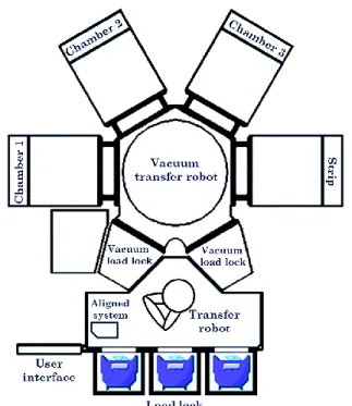
2. PLASMA ETCH EQUIPMENT ...47
2.1. The Etch Platform ...47
2.1.1. Lam Versys 2300 Etch Chamber ...48
2.1.2. Process Etch and Chamber Conditioning ...49
3. DIAGNOSTIC TECHNIQUES ...52
3.1. End Point Detection Technique (EPD) ...53
3.1.1. What is an Endpoint? ...53
3.1.2. Light Signal Reflectometry (LSR)...54
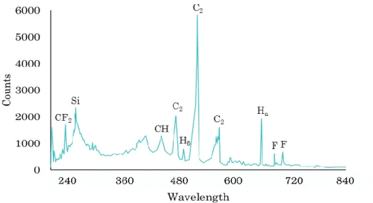
3.1.3. Optical Emission Spectroscopy (OES) ...56
3.2. Scatterometry ...60
3.2.1. Principle ...61
3.2.2. Instrumentation ...61
3.2.3. New Model for STI Measures ...62
3.3. X-Ray Photoelectron Spectroscopy (XPS) ...63
3.3.1. Principle ...63
3.3.2. Instrumentation ...65
3.3.3. Spectral Analysis ...65
3.3.4. Angle-Resolved XPS (ARXPS) ...67
3.3.5. Floating Sample Method ...68
3.4. Scanning Electron Microscopy (SEM) ...70
3.5. CD-Scanning Electron Microscopy (CDSEM) ...71
3.6. Transmission Electron Microscopy (TEM) ...71
3
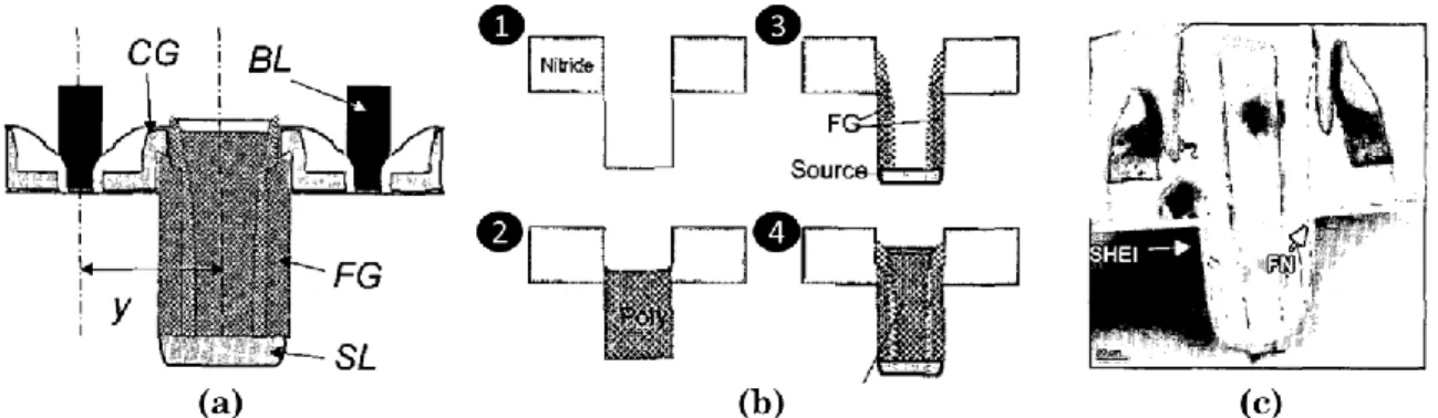
1.1. Embedded Select Trench Memory (eSTM) ...74
1.1.1. The Starting Point: The 2T cell ...75
1.1.2. Literature Review of the Polysilicon Vertical Trenches ...75
1.1.3. The Polysilicon Trench of the eSTM: The Vertical Transistor ...78
1.2. Plasma Etching Considerations ...79
1.2.1. Pure Plasma Chemistries ...80
1.2.2. Etch Directionality in RIE ...82
1.2.3. Etch Selectivity in RIE...83
1.2.4. Literature Review on the Mechanistic Studies of Si and SiO2 Etching ...83
2. EXPERIMENTAL APPROACH...90
2.1. Fabrication Process ...90
2.1.1. The Necessary Steps for Reaching the eSTM Trench ...90
2.1.2. The Selected Chemistry for the eSTM Trench ...91
2.2. Specifications ...93
2.2.1. Stack ...93
2.2.2. Etching Specifications ...93
2.2.3. Morphological Study of each Step ...95
3. CHARACTERIZATION ...96 3.1. Plasma Diagnostics ...96 3.1.1. Background ...97 3.1.2. Experimental ... 100 3.1.3. Results ... 102 3.1.4. Summary ... 107 3.2. Surface Characterization ... 107 3.2.1. Background ... 108 3.2.2. Experimental ... 112 3.2.3. Results ... 114 3.2.4. Discussion ... 129
4
4.2. Experiments ... 135
4.2.1. Choice of the Factors ... 136
4.2.2. Design of Experiments ... 141
4.3. Results ... 143
4.3.1. DOE Analysis ... 143
4.3.2. Predictions and Validation ... 146
4.3.3. Further Details ... 147
4.4. Summary and Industrialization ... 149
5. CONCLUSION ... 150
IV. Plasma-Reactor Walls Interactions: The Fluorine Problem ... 153
1. LITERATURE REVIEW ... 154
1.1. Influence of Reactor Wall Conditions on Etch Processes ... 154
1.2. Contamination: The Fluorine Problem ... 156
2. PROCESS AND CLEANING CONSIDERATIONS ... 157
3. CHARACTERIZATION ... 158 3.1. State-of-the-art ... 158 3.2. Experimental ... 160 3.2.1. Substrates ... 162 3.3. Results ... 162 4. OPTIMIZATION ... 165 4.1. State-of-the-art ... 165 4.2. Strategy... 167 4.2.1. Protocol ... 167 4.3. Results ... 168 5. CONCLUSIONS ... 171
5
1.1. The STI Process ... 174
1.2. Process Variation ... 175
1.2.1. Measures of Variation ... 176
1.3. Process Control in Semiconductor Manufacturing ... 177
1.3.1. Statistical Process Control (SPC) ... 177
1.3.2. Advanced Process Control (APC) ... 178
2. EXPERIMENTAL ... 180 2.1. Stack ... 180 2.2. Etching Specifications ... 181 2.3. Industrial Context ... 182 3. CHARACTERIZATION ... 182 3.1. Process Variability ... 182
3.2. Impact of Previous Steps ... 183
3.3. The Influence of Etching ... 187
4. OPTIMIZATION ... 188
4.1. The EWMA R2R Strategy ... 189
4.2. The STI-Etch R2R Controller ... 190
4.2.1. R2R Operation ... 191
4.2.2. Model Validation ... 193
4.2.3. New Metrology ... 194
5. CONCLUSIONS ... 195
Conclusions and Future Work ... 197
Résumé (French) ... 201
Bibliography ... 231
7
The work presented in this thesis was carried out by the author, with the following exceptions: Process
1. All the CMOS processes were done at STMicroelectronics Rousset. All the etching steps were performed by the author.
2. Al2O3 depositions were provided by ENCAPSULIX SAS.
3. Y2O3 substrates were provided by Pr. Rolly GABORIAUD, Departement Physique et Mecanique des
Materiaux, CNRS-Universite de Poitiers. Characterization
1. SEM, TEM and EDX images of full devices were taken at the ST Rousset characterization laboratory. 2. XPS analyses realized at CIMPACA were carried out by B. Bortolotti and A. James.
3. Electrical measures of the devices were made by the electrical characterization group at ST Rousset. 4. The scatterometry model was developed with Julian Martinez (metrology group).
5. The R2R was developed in collaboration with Dennis Pompier (automation team).
8
Acronyms
a-C:H Amorphous Hydrogenated Carbon AHM Ashable Hard Mask
ARXPS Angle-Resolved X-ray Photoelectron Spectroscopy BEOL Back End of Line
BL Bit Line BT Breakthrough CD Critical Dimensions
CD-SEM CD- Scanning Electron Microscopy CG Control Gate
CMOS Complementary Metal-Oxide Semiconductor CMP Chemical-Mechanical Polishing
CVD Chemical Vapor Deposition DOE Design of Experiment DTI Deep Trench Isolation
ECR Electron Cyclotron Resonance EDX Energy Dispersive X-ray spectrometry
EEPROM Electrically Erasable Programmable Read Only Memory eSTM Embedded Select Trench Memory
FEOL Front End of Line FG Floating Gate
FN Fowler Nordhein IC Integrated Circuit
ICP Inductively Coupled Plasma
ITRS International Technology Roadmap for Semiconductors ME Main Etch
MOS Metal-Oxide Semiconductor
MOSFET Metal-Oxide-Semiconductor Field Effect Transistor NVM Non-Volatile Memory
OE Over Etch
OES Optical Emission Spectroscopy ONO Oxide-Nitride-Oxide
PECVD Plasma Enhanced Chemical Vapor Deposition PW/NW P-Well/N-Well
PVD Physical Vapor Deposition RAM Random Access Memory RF Radio-Frequency
RIE Reactive Ion Etching ROM Read Only Memory R2R Run-to-Run
SEM Scanning Electron Microscopy SHEI Substrate Hot Electron Injection SL Source Line
STI Shallow Trench Isolation TCP Transformer Coupled Plasma TCR Top Corner Rounding
TOFSIMS Time of Fly Secondary ion mass spectroscopy WL Worl Line
9 The Critical Dimension (CD) is highly influenced by the Reactive Ion Etching (RIE) of silicon in the CMOS technology. The CD has to be well-controlled since it is one of the most important features related to process stability and product quality. However, the RIE process involves a lot of parameters which are highly confounded and entangled and thus it is very difficult to analyze the process. The main objectives of this thesis are to have an understanding of the fundamental mechanisms of the etching process and to propose innovative solutions to reduce the variations of CD by reaching the good control of the process desired.
This research was carried out in parallel between STMicroelectronics Rousset and the Center Microelectronic of Provence (CMP).
The structure of this thesis is organized in five chapters. The experimental results of this study are presented through chapters III to V (Figure 1). These chapters begin with an introduction to the relevant literature and the experimental details related to the process. Then, the results are expressed in two parts; the characterization and the optimization of the process. A summary of the result is presented at the end of each part and finally the conclusions are drawn.
10
The main propose of each chapter is:
In Chapter I, the main aspects and actual tendencies in CMOS technology and plasma etching is introduced.
Chapter II, describes the experimental systems regarding the plasma etching equipment and the characterization techniques.
Chapter III, is dedicated to a detailed understanding of the main mechanism involved in the etching of the mask and specially the silicon during the etch of the new vertical transistor of the eSTM structure. Characterizations of the plasma itself, and the surface of the wafer are discussed. After understanding the mechanism involved in this process, a model able to predict the optimum CD in terms of electrical results is proposed by means of DOE.
Chapter IV, presents to the characterization of the reactor walls during the eSTM process. Since this technology is still in development, the cleaning recipe has to be optimized in order to get the best results without contaminating the chamber from process to process due to fact of working in an industrial environment (ST Microelectronics).
Chapter V, contains the study of the source of variability during the STI trench etch process. The development of a R2R control for the CD of this trench to improve the uniformity 3sigma total of the CD is described.
Finally, the main conclusions are summarized, as well as the proposition of the possible applications of the results obtained and future directions of this work.
11
“Science knows no country, because knowledge belongs to humanity, and is the torch which illuminates the world” (L. Pasteur)
Chapter I
Introduction
This chapter presents the general motivation of this thesis, based on the
past and present state-of-the-art related to the plasma etching in
semiconductor manufacturing. An overview of the microelectronics with
emphasis in the CMOS technology will be introduced followed by some of
the most important plasma etching concepts. Finally, the objectives of the
thesis are presented.
12
Great advances in semiconductor technology and circuit design techniques have been observed in recent years. Yet, chip manufacturing is a very challenging undertaking, primarily because of the complexity and sensitivity of its production process [1].
1. MICROELECTRONICS: AN OVERVIEW
As the name suggests, microelectronics is related to the study and manufacture of very small electronic designs and components. Over the last decades, the semiconductor industry has played a major role in social and economic development since the invention of the transistor. Every remarkable modern innovation has been made possible by the transistor, but they are most commonly known for their contribution to the world of computers.
The beginning of semiconductor research is well established by the mid-1930s, when the quantum theory of solids began to be interesting to industrial scientists seeking solid-state alternatives to vacuum-tube amplifiers and electromechanical relays [2]. In 1947, the most important invention of the past century, the transistor, emerges from the Bell laboratories by J. Bardeen, W. Brattain and W. B. Shockley. Eleven years later, in 1958, Jack Kilby created the first Integrated Circuit (IC) while working at Texas Instruments laboratories [3]. Up to 1970 the integrated circuit’s innovation and business was almost completely a U.S. phenomenon. In 1971, appears the first commercially microprocessor by Intel which held 2300 transistors and announcing a new era in Integrated Electronics [4]. Figure I-1 shows the first Integrated Circuit from Texas Instrument (1958) and the first microprocessor from Intel (1971).
Figure I-1. First Integrated Circuit Texas Instruments, 1958 (source: Texas Instruments) and first microprocessor Intel, 1971 (source: Intel).
As the semiconductor technology improved, the technology of transistors grew making them faster, cheaper, smaller and more reliable. The object was to miniaturize electronics equipment to include increasingly complex electronics functions in limited space with minimum weight.
According to the empirical theory of Gordon Moore in 1965 [5], the number of transistors on an Integrated Circuit (IC) roughly doubles every year, whereas the cost per transistor is
13 reduced at the same time. Ten years later, in 1975, he reformulated this theory explaining that the number of transistors per integrated circuit doubles every 18 months.
This prediction has been surprisingly accurate. As a result, the scale gets smaller, and transistor count increases at a regular pace to provide improvements in IC functionality and performance while decreasing costs. The exponential growth that continues today is shown in Figure I-2.
Figure I-2. Moore’s Law for transistor counts since 1970 [Data from 6].
Since 1977, the Moore’s law is showed as a technology roadmap in the International Technology Roadmap for Semiconductors (ITRS) where the evolution of the microelectronics is predicted in a short, medium and long term [7]. The ITRS synchronizes the technology development and the timely availability of manufacturing tools and methods. However, as the physical limits are approached, other factors such as design cost, manufacturing economics and device reliability, make progress through device scaling alone ever more challenging, and alternative ways forward must be sought [8].
Microelectronics therefore seeks to develop in new ways for keeping the miniaturization going, as it has been coming until now. This miniaturization has been possible thanks to the control of processes implied on the fabrication of Integrated Circuits based on CMOS technologies.
14
2. CMOS TECHNOLOGY
CMOS (Complementary Metal-Oxide Semiconductor) is the semiconductor technology used in the transistors that are manufactured into most of today’s computer microchips such as microprocessors, microcontrollers, static RAM and other digital logic circuits. CMOS derives its name from the basic physical structure of these devices; the MOS capacitor, composed of a semiconductor, oxide and a metal gate.
In the following sections, some key aspects of this technology will be discussed. In the first section a quick overview of CMOS basics is given, such as the principal element used in microelectronics, the integration of this element into the technology and the classification of semiconductor memories. The second will deal with the fabrication process and finally, the role of plasma etching in CMOS technology is shown.
2.1. Basics
The most basic element in the design of a large scale integrated circuit is the transistor. For the processes we will discuss, the type of transistor available is MOSFET [9,10], which becomes imperative when the problems of high power consumption become dominant. Even if the bipolar transistors are faster than MOSFET’s, these devices have low power consumption and can be scaled down easily than other transistor types. MOSFET is a compromised of an MOS capacitor (gate and substrate terminals) and two pn junctions (source and drain terminals) as illustrated by Figure I-3. The MOS capacitor [10,11,12] consists of a Metal-Oxide-Semiconductor structure. It is actually a “sandwich” consisting of the underlying substrate material, which is a single crystal of semiconductor material (usually silicon heavily-doped); a thin insulating layer (usually thermal silicon dioxide); and an upper metal layer.Actually, the transistors that we will discuss do not use metal for their gate regions, but instead use heavily-doped polycrystalline silicon (Poly-Si).
15 As capacitor, the MOS is able to store charge; however, the MOSFET, as transistor, acts as a current switch and amplifies the current. The electrical charge, or current, can flow from the source to the drain depending on the charge applied to the gate region. Details of the MOSFET structure and physical operation are explained in 2.1.1.
Almost universally, the MOSFET structure utilizes doped silicon as the semiconductor on the substrate and its native oxide, silicon dioxide, as the insulator. The semiconductor material in the source and drain regions is “doped” with a different type of material than in the region under the gate, so an NPN or PNP structure exists between the source and drain regions [10,13,14,15].
The most commonly used semiconductor since the early 1960s is silicon (Si) [16,17] which is today the cornerstone of modern CMOS technology. The main reasons we use silicon [18] are that silicon devices exhibit better properties at room temperature, and high-quality silicon dioxide can be grown thermally. There is also an economic consideration, device-grade silicon cost much less than any other semiconductor material [19].
Semiconductors [20] are a group of materials having conductivities between those of conductors and insulators. Silicon atoms form covalent bonds and can crystallize into a regular lattice. Each of these elements has four valence electrons and needs four more to complete the valence energy shell. If a silicon atom, has four nearest neighbors, with each neighbor atom contributing one valence electron to be shared, then the atom of the center will have eight electrons in its outer shell.This structure is called an intrinsic semiconductor and can conduct a small amount of current. In intrinsic semiconductors, the conductivity is determined by both electrons and holes and depends on the carrier density. A two-dimensional representation of the covalent bonding in silicon is shown in Figure I-4.
Figure I-4. 2DSchematic representation of the covalent bonding in silicon.
It is possible to shift the balance of electrons and holes in a silicon crystal lattice by "doping" it with other atoms. This doping process, described in [21,22],can greatly alter the electrical characteristics of the semiconductor. Semiconductors in its pure form are called intrinsic whereas that impure semiconductors are called extrinsic.
Depending on the type of impurity added we have two types of semiconductors: N-type and P-type. An extrinsic semiconductor will have either a preponderance of electrons (n-type) or a preponderance of holes (p-type). These effects are schematically shown in Figure I-5.
16
Figure I-5. Representation of the intrinsic silicon lattice (a), N-doped Si (b), P-doped Si (c).
Atoms with more valence electrons than silicon, mainly from group V [23], are used to produce “n-type” silicon material, which adds electrons to the conduction band and hence increases the number of electrons. Atoms with less valence electrons than silicon, mainly from group III [24], result in “p-type” silicon material. In p-type, the number of electrons trapped in bonds is higher, thus effectively increases the number of holes. Table I-1 summarizes the properties of semiconductor types.
Table I-1. Properties of P-type and N-type semiconductors.
P-type (positive) N-type (negative) Dopant Group III (e.g. Boron) Group V (e.g. Phosphorous)
Valence Electrons 3 5
Polarity Positive Negative
Charge carriers Missing Electrons (Holes) Excess Electrons
The intrinsic silicon is not useful due to the low conductivity. The extrinsic semiconductors are the primary reason we can fabricate the various semiconductor devices [25] that we will consider in this thesis.
2.1.1. The MOSFET Structure and Principle of Operation
The Metal-Oxide-Semiconductor Field Effect Transistor (MOSFET) is by far the most common type of transistor. The basic MOSFET structure was proposed by Atalla [26], but the first MOSFET transistor was reported in 1960 by Kahng and Atalla [27].
As explained before, it is a compromise between a MOS capacitor and two pn junctions: the Source and the Drain (S/D). These regions, heavily-doped, are quite similar and are labelled depending on what they are connected to. The source is the terminal or node, which acts as the source of charge carriers. The charge carriers leave the source and travel to the drain. In the case of an N channel MOSFET, the source is the more negative of the terminals; in the case of a P channel, it is the most positive of the terminals. The area under the gate oxide
17 is called the “channel”, which is lightly doped. Table I-2 summarizes the properties of the transistor types [28].
Table I-2. Composition of NMOS and PMOS.
Transistor type S/D channel Inversion layer created
NMOS n-type p-type n-type
PMOS p-type n-type p-type
The basic device parameters are the channel length L, which is the distance between the two metallurgical n+-p junctions; the channel width W; the insulator thickness d and the substrate doping NA. In a silicon integrated circuit, a MOSFET is surrounded by a thick oxide
(called the field oxide to distinguish it from the gate oxide) or a trench filled with insulator to electrically isolate it from adjacent devices [10]. The insulation trenches that isolate the different transistors between them are called STI (Shallow Trench Isolation). The basic structure of a MOSFET is illustrated in Figure I-6.
Figure I-6. Schematic diagram of a basic MOSFET [Adapted from10].
MOSFET works [13,29] by electronically varying the width of a channel along which charge carriers flow (electrons or holes). The charge carriers enter into the channel trough the source and exit via the drain. The width of the channel is controlled by the voltage on the gate. The flow of the current between the source and the drain depends on the voltages that are applied to these terminals.
Corresponding to whether the transistor is in an ON state or an OFF state at zero gate– source voltage, two basic forms of MOSFET are available [30,31]: “Depletion-mode” and “Enhancement-mode”. A channel marks the main difference between the two types (the so-called conducting “path”). It is located between the source and drain. With the depletion-mode MOSFET it is formed in the doping process during fabrication. In the
enhancement-18
mode device there is no channel between the source and drain. Both types of MOSFET devices have either an n-channel or a p-channel depending on their added impurities. However, MOSFET is a unipolar device, its operation depends on only one type of charge, either electrons or holes, but never both.
The operational principle of MOSFET depends on the MOS capacitor, since it is the main part of the device. We will consider subsequently the case of an n-MOS as an example. MOSFET having n-channel region between source and drain is a four terminal device, where the terminals are gate, drain, source and substrate or body. The drain and source are heavily doped n+ region and the substrate is p-type. The current flows of the negatively charged electrons, that is why it is known as n-channel MOSFET. When we apply positive voltage to the gate, the holes present beneath the oxide layer experience repulsive force and they are pushed downwards in to the bound negative charges which are associated with the acceptor atoms. The positive gate voltage also attracts electrons from n+ source and drain region in to the channel, thus the electron rich channel is formed. Now, if a voltage is applied between the source and drain, current flows freely between them. The gate voltage controls the electron concentration in the channel. N-channel is preferred over p-channel MOSFET as the mobility of electrons are higher than holes [32]. The diagrams of enhancement mode and depletion mode for an n-MOS are given in Figure I-7.
Figure I-7. Schematic of n-MOS in depletion-mode and enhanced-mode [Adapted from 32].
CMOS circuits require n-MOS and p-MOS transistors, the integration of these transistors on the same substrate for CMOS processes is explained in next section.
2.1.2. From MOS to CMOS
MOSFET is the most-important device for forefront high-density integrated circuits such as microprocessors and semiconductor memories. These circuits, fabricated with the CMOS technique, require an nMOS and pMOS transistor technology on the substrate to enable the logic functions. To this end, an n-type is usually provided in the p-type substrate or an n-type and p-type in a low-doped substrate.
19 The advantage of CMOS is that the output can be as high as the power supply voltage and as low as ground. In addition, there is no power dissipation in either logic state. Instead the power dissipation occurs only when a transition is made between logic states. CMOS circuits are the most suited for very/ultra-large-scale integration (VLSI/ULSI) [29,33].
Several applications are possible such as microprocessors, microcontrollers and other digital logic circuits [34-37]. Even if this technology is also used for several analogy circuits, one of the most widespread is the microprocessor, which takes several million transistors and at least 10 levels of metal for the interconnections. Figure I-8 shows the photograph of a microprocessor including in the same circuit the microcontroller (logic) dedicated to the processing of inputs and outputs and the memory where the information is stored.
Figure I-8. Microprocessor including the memory and the logic.
The microprocessor allows managing a large amount of stored data in the RAM (Random Access Memory) memory cells, the so-called Volatile Memories. The memory part used to stock the information is the so-called Non Volatile Memory (NVM) [38-41]. As the names imply, a volatile memory loses the content when there is no voltage whereas a nonvolatile memory does not need voltage to maintain the data.
As the memory market enters the Gigabit and GHz range with consumers demanding ever higher performance and more diversified applications, new types of devices are being developed in order to keep up with the scaling requirements for cost reduction [42]. In this scenario, memories [43,44] play an important role. The most important semiconductor memories will be summarized in the next section.
2.1.3. Semiconductor Memories
Semiconductor memories can be classified by regarding different criteria, Figure I-9 shows a first classification of these memories.
20
Figure I-9. Classification of semiconductor memories.
The Volatile Memories are fast and are used for temporary storage of data since they lose the information when the power is turned off. This means that they need to be permanently under tension to keep their information. The Non Volatile Memories (NVM) [39,49] retain the information even when the power is down. They have been conceived in order to store the information without any power consumption for a long time.
The first Non Volatile semiconductor memory is the ROM (Read Only Memory). This new device appears when the gate electrode of a conventional MOSFET is modified so that semipermanent charge storage inside the gate stack is possible. Since the first nonvolatile memory device proposed by Kahng and Sze in 1967 [50] various device structures have been made, and nonvolatile memory devices have been extensively used in commercial products. The two groups of nonvolatile memory devices are the floating-gate devices [51] and the charge-trapping devices [52].
The characterization and optimization which have been carried out during the development of this thesis is related to the Floating-gate’s structure, but before getting into details about the memories studied here, we should first clarify what a Floating gate transistor is. A floating gate is basically a MOSFET with two supplementary levels of polysilicon. These two levels of polysilicon are separated by a tri-insulating layer of ONO (Oxide / Nitride / Oxide), whose role is to prevent the pass from the floating-gate to the control-gate.
For the understanding of this thesis, the difference between the EEPROM and the Flash memories, both of them floating-gate based, should be introduced. The basic structure of each memory is presented in Figure I-10 and the main different between these two NVM are explained as follows:
EEPROM (Electrically Erasable Programmable Read Only Memory). An electrically erasable/programmable ROM, can be erased not only electrically, but also selectively by byte address. To erase selectively, a select transistor is needed for each cell, leading to a two-transistor cell (2T); the floating-gate and the select-transistor.
21 The select transistor increases the size of the memories and the complexity of array organization, but the memory array can be erased bit per bit.
Flash memory. The name “flash” comes from its fast erasing mechanism. It looks like EEPROM memory but without the select transistor. As opposed to a full-feature EEPROM, can be erased electrically but only by a large block of cells simultaneously. It loses byte selectivity but maintains one-transistor cell (just the floating-gate). Today it is the most produced memory.
Figure I-10. Schematic of EEPROM (a) and Flash (b) memories.
Among other characteristics, the ideal memory should have low power consumption, fast read/write/erase and high density solution… But the “ideal” device does not exist yet. However, different types of memories have been invented in order to pursuit these specific properties [43,44]. Example of this attempt is the eSTM (Embedded Select Trench Memory) which is represented in Figure I-11. This memory has been presented by STMicroelectronics in 2012 [53,54].
Figure I-11. Schematic of eSTM structure.
The eSTM aims to have the advantages of consumption and isolation from the EEPROM, due to its select transistor, together with the advantage of the Flash by reducing its size. Based on this, two select-transistors have been merged into a single vertical transistor of selection.
22
Thanks to this, it is possible to convert a large cell (2T) as the EEPROM, into a new cell, smaller in size and still with low consumption, at the expense of a slightly more complex manufacturing process but still compatible with a CMOS technology. The properties of EEPROM, Flash and eSTM memories are compared below in Table I-3.
Table I-3. EEPROM, Flash and eSTM properties.
EEPROM FLASH eSTM
Low Consumption x x
Fully-Bit alterable x x
High Density x x
Fast Write/Erase x x
The main characteristics of this new structure are:
A vertical transistor, used as the selection transistor.
The Niso, serving to isolate transistors to the substrate, is also used in the eSTM as a source line to win a contact.
Two floating gate transistors, with a length of 100 nm, presented on either side of the selection transistor separated by an N+ implant.
The trench where the select-transistor will be placed consist of 450nm of depth (corresponding to the Niso) and 150 nm of width.
In this thesis, two different trenches have been studied. Chapter III and Chapter IV are related to the characterization and optimization of the eSTM trench process; Chapter V will be focused on the STI trench. Details of those fabrication processes will be explained in their respective chapters, but first it is important to present the basic steps of the fabrication processes in CMOS technology that all these structures follow.
2.2. Fabrication Processes
Integrated-circuits are now fabricated industrially by using wafers. Wafers are thin circular slices, usually of monocrystalline silicon. On each wafer hundreds or thousands of individual chips are fabricated, as represented in Figure I-12. Technically, each of these individual chips is called die, and each die might represent an Integrated Circuit (IC) [55]. For economic reasons, the size of the wafer increases gradually on the semiconductor manufacturing industries, up to 300mm today. Due to the size of the devices on the IC, it is essential to work in a very-clean environment, the so-called clean room, keeping temperature and humidity under control in order to prevent the contamination that could damage the functionality of the circuit.
23 Figure I-12. Representative drawing of a die.
Complex technologies might have more than 40 layers, which implies more than 400 successive process steps. These steps can be segmented into different families [19,56,57,58]. Epitaxial growth. It consists in growing a crystal of a material onto another
material.
Ion Implantation or Doping. To introduce chemical elements in the substratum material in order to obtain the right electrical properties (i.e., specific regions with positive or negative charge).
Thermal treatment. By increasing the temperature of a substrate under controlled atmosphere in order to change its properties.
Deposition. Thin films of different materials are deposited on the wafer through several processes, such as: Chemical Vapor Deposition (CVD), Physical Vapor Deposition (PVD), Plasma Enhanced Chemical Vapor Deposition (PECVD) and Metallization.
Lithography. It is used to add patterns on the wafer. First, the wafer is coated with a film of photosensitive polymer. Then, the pattern is transferred from a photo mask onto the photosensitive polymer by projecting light through the mask and exposing the wafer using ultraviolet light. Finally, the polymerized sections of photoresist material are removed from the wafer to develop the pattern.
Etching. With the etch processes, the areas defined by the patterns can be removed. Etching can be wet or dry. In wet etching, liquids are used such as acids, bases and solvents to chemically remove wafer surface material. In dry etching or plasma etching, the wafer surface is exposed to a plasma. Plasma etching is the most common etch process and since it is the object of study in thesis, details about this step will be developed in 3.
Planarization of the surface. In order to achieve a flat layer, the wafer surface is polished. This is critical for the follow-on process steps (e.g. better linewidth control during photolithography) and can serve to increase device yields by removing
24
undesirable foreign material on the wafer surface. Usually by Chemical-Mechanical Polishing (CMP).
Cleaning. It consists in removing any residue from the material surface.
There are two classes of processing steps in the manufacture of an integrated circuit: those concerning the implementation of active devices, the so-called "Front End of Line" (FEOL) and those related to the achievement of interconnections between these devices to get the expected logic function, known as "Back End of Line" (BEOL). Details about the FEOL and BEOL are introduced in the next sections.
2.2.1. Front End of Line (FEOL)
This thesis focuses on the FEOL. Therefore, we introduce the different processes performed during the wafer fabrication, which is characterized by its complexity and highly expensive processes. In order to design MOS transistors various successive steps are performed such as [29]:
- Starting material, called “substrate” or “well”. Consists of the selection of the type of wafer to be used, the CMP and cleaning of the wafer.
- Shallow Trench Isolation (STI) module. Creation of regions of dielectrics between regions of active areas. The regions of dielectrics, called STI, are not very deep trenches filled with SiO2 in order to electrically isolate the transistors from each
other.
- Well module. The “wells” are formed by creating n-type or p-type by means of implantation of Phosphorus (P) or Boron (B). The non-implanted areas are protected by a photoresist. This will allow the opposed conduction type respect to the transistor that will be created in this area.
- Gate module. The formation of the gate (N- or P-channel) which is the control electrode of the transistor.
- Source/Drain module. The Source as the Drain will receive the implantation N for a N-MOS transistor and P for a P-MOS. The non-implanted area, as it is the case for the STI, are protected by a photo-resist. The formation of the S/D take place in two parts. First, there is a Lightly Doped Drain (LDD) implantation, as a extension of the S/D. After that, the creation of “spacers”-explained below- is carried out before the second implantation. For the second implantation, the dose is incremented and the area is limited by the spacers. Here, the S/D regions themselves are created.
- Spacers. Two spacers are created on either side of the gate, allowing its alignment with the source/drain during the production and the limitation of the second implantation under the gate.
- Siliciding. This step is performed in order to reduce the contact resistance of the gate, source and drain.
25 After these steps, the transistors will be obtained as represented in Figure I-13. In order to perform these transistors, all the different fabrication processes explained before (such as deposition, lithography, etch, etc) are required. Specifications related to the etching of the trench for the different technologies studied in this thesis will be introduced at the beginning of each chapter.
Figure I-13. Representation of MOS transistors at the end of the FEOL steps.
Major differences in the design of the FEOL are often due to the specific technology requirements.
2.2.2. Back End of Line (BEOL)
Once the various semiconductor devices have been created, they must be interconnected to form the desired electrical circuits. This occurs in a series of wafer processing steps called BEOL, which normally begins when the first layer of metal is deposited on the wafer. The BEOL will help to achieve the metal interconnections between the individual devices by creating interconnect wires, vias and dielectric structures. These interconnections are organized on several levels which are interconnected from each other by means of insulating trenches of a dielectric material. Current technologies use up to 12 levels of interconnections. Conventionally, aluminum (Al) metallization contact are used for these interconnections. However, higher performance BEOL are implemented using a Cu for the respective conducting and insulating materials, since the electrical conductivity of Cu is higher than the one of Al [58]. When the BEOL is finished, there is a “back-end process” also called “post-fab” since it is carried out not in the cleanroom.
2.3. The Role of Plasma Etching in CMOS Technology
Silicon-based CMOS technology has been the main force driving the progress of the microelectronics industry for over four decades. The remarkable decrease in design rule and increase in the number of components on an individual integrated circuit required a major change in the technology used to fabricate such circuits. By subsequent etching and deposition of patterns, the microelectronic devices like transistors and the interconnecting
26
lines are produced on a semiconductor substrate as it has been explained before. The main steps such as deposition, lithography and plasma etching, are sketched in Figure I-14.
Figure I-14. Representation of the main microelectronics fabrication steps [Adapted from 59].
During the etching, the silicon is reached, as Figure 1-14 shows, this is why a good control of this process had to be developed. In the earliest days of large-scale integration, isotropic wet chemical etching was sufficient to produce the patterns required. As commercial pressures forced the industry to ever smaller design rules, the limitations of wet chemical etching became progressively less satisfactory and this is why dry etching or plasma etching became a technology essential to microelectronics circuit fabrication [60-61]. Figure I-15 illustrates the differences between wet and dry etching.
Figure I-15. Sketch of an isotropic wet etch process and an anisotropic dry etch process [Adapted from 59].
Nowadays, one of the principal challenges at the nanoscale faced by the semiconductor industry is the device fabrication [19] and the control of variations at the nanoscale [62-64]. To address this challenge, plasma etching is widely investigated [59,65,66,67]. Likewise, plasma etching is the object of this research so that an introduction to the plasma etching in microelectronic and its state-of-the-art will be presented in the next section.
27
3. PLASMA ETCHING
Plasma or dry etching of silicon plays a major role in semiconductor manufacturing. It consists in allowing the transfer of complex circuit patterns by photolithography to the silicon, silicon dioxide, and metals that build the integrated circuits.
3.1. Introduction
The first use of the term “Plasma” in literature is dated 1928 [68] when Irving Langmuir designates it as a partially ionized gas. More accurately, a plasma [69] is a gas containing charged and neutral species, including some or all of the following: electrons, positive ions, negative ions, atoms and molecules, that show a collective behavior. Plasma is one of the four fundamental states of matter, the other being solid, liquid and gas; but plasma has properties unlike those of the other states. Besides, it is the most abundant form of ordinary matter in the universe. The 99% is plasma such as the starts, the solar core, the aurora, etc. On earth, plasmas are used in domestic appliances like neon tubes; for energy production like fusion reactor and for surface treatments like depositing thin films and etching materials. Etching materials with plasma has become a key process for removing material from surface in CMOS manufacturing.
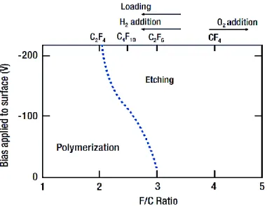
Much of the understanding of plasmas has come from the pursuit of controlled plasma etching processes for CMOS technology, where the plasma generation [70] requires the application of strong Radio Frequency (RF), under vacuum conditions. The main advantage of using dry etching against wet etching relies on the possibility that plasma etching offers of anisotropic etching (Figure I-15), which is highly preferable for smaller feature dimensions. Furthermore, anisotropic etching has the ability to etch with finer resolution and higher aspect ratio than isotropic etching. So, by the late 1970s, the microelectronics industry drives the transition from wet etching to plasma etching, and nowadays almost all the pattern-transfer processes are done by plasma etching. The possibility of anisotropic etching comes from the two approaches, physical and chemical, that this process implies. The physical part (3.3) can be accomplished by neutral, ion, electron or photon bombardment that assisted etching reactions of a surface exposed to a chemical etchant. It is anisotropic and non-selective. The chemical part (3.4) involves a chemical reaction between etchant gases to attack the silicon surface. It is spontaneous, isotropic and exhibits high selectively.
Coburn and Winters, in their classical experiment in 1979 [71] showed that plasma etching is the synergetic result of the combination between these two mechanisms; the ion bombardment and the neutral chemical reaction.
28
In the following sections, the main aspects of plasma etching will be discussed. The first one is about the basic properties of plasmas, since they are required for plasma etching processes. Then, the physical and chemical interactions at surfaces in contact with plasmas are discussed. Finally, the state-of-the-art in plasma etching is introduced.
3.2. Basic Plasma Properties
There are several textbooks that provide very comprehensive introductions to plasma physics
[72-75]. In this section, the fundamental plasma discharge concepts which underlie the
operation of plasma etching will be discussed.
To form and sustain, a plasma requires some energy source to produce the required ionization, the degree of ionization is an important parameter of a plasma (I.1). The plasmas used in the semiconductor industry are weakly ionized plasma discharges because the degree of ionization is around 1 out of every 10,000 at most. The majority of the particles remain neutral, and only one ion and one electron exist for every 10,000 neutral particles [61]. The degree of ionization [76] of a plasma is defined as:
Degree of ionization:
=
𝑛𝑖𝑛𝑖+𝑁𝑔 (I.1)
where, 𝑛𝑖 is the ion density (cm-3), 𝑁
𝑔 is neutral species density (cm-3)
Therefore, if is zero, then the gas is called neutral. However, if = 1 then the plasma is completely ionized. The electron density (ne) is related to this by the average charge state of
the ions (Z) through (I.2.):
𝑛
𝑒= 𝑍 ∙ 𝑛
𝑖 (I.2)The electron density (ne) and ion density (ni) are substantially equal to one another, ni≈ne, a
condition commonly termed “quasi-neutrality”
[
77
]
. Because electrons are able to travel freely within the plasma, it has a conductive property. When a radiofrequency (RF) power is applied on a pair of electrodes in an etch chamber, electrons are accelerated by an electric field generated by the RF power, acquire kinetic energy, and collide with atoms and molecules to cause ionization, excitation, dissociation, etc (3.3.3). But even if in the RF electric field, the electrons are continuously accelerated, they have much smaller mass than atoms and so they can only transfer small amounts of energy in collisions. As a result, the different plasma species have different kinetic energies and thus different temperatures. This means that they are not in a thermodynamic equilibrium. Typically, one can only speak of temperature if the particles are in equilibrium between each other. However, it is possible to set a temperature for each of these species by making the approximation that the particles have an energy29 distribution according to the Maxwell-Boltzmann distributions
[
78
]
. This means that there is a thermodynamic equilibrium within each specie.Based on the relative temperatures of the electrons (Te), ions (Ti) and the neutral gas (Tg),
plasmas are classified as thermal or non-thermal. Thermal
[
79
]
plasmas have electrons andthe heavy particles at the same temperature while that non-thermal
[
80
]
plasmas have theions and neutrals at a much lower temperature (often near the ambient temperature),
whereas electrons are much "hotter" (Te>>Tg). Other definition based on the electronics
temperature of a plasma (I.3), is referred to as being hot
[
81
]
if it is nearly fully ionized, orcold
[
82
]
if only a small fraction (for example 1%) of the gas molecules are ionized. In theliterature, it can be also referred as hot plasma (T>106 K) and cold plasma (T<106 K). Plasmas
utilized in semiconductor manufacturing are usually cold plasmas since only a small fraction
of the gas molecules are ionized. Furthermore, for these plasmas Te>>Ti.
Electronic temperature:
𝑇
𝑒(𝑒𝑉) =
𝑘𝐵𝑒
𝑇
𝑒(𝐾)
(I.3)where, 𝑘𝐵 is the Boltzmann constant (𝑘𝐵= 1,38 ∙ 10−23 𝐽. 𝐾−1) 𝑒 is the elementary charge (𝑒 = 1,6 ∙ 10−19 𝐶)
As explained before, the electrons have much smaller mass than atoms and thereby they are
much faster. Because of that, the flux to the walls of the electrons should be as well much bigger and thereby the plasma would not be neutral. To preserve its “quasi-neutrality”, the plasma is protected by forming a load zone of positive space, called sheath. Due to this sheath, the plasma has higher potential (Vp) than the walls. The plasma is brought to a potential
Vp>0 which will make that more electrons are retained in the plasma and more ions are
accelerated to the walls. The sheath has a minimal thickness that is on the order of the Debye length (λD). The Debye length describes the distance over which an electrical disturbance is
screened in a space charge as defined in (I.4).
Debye length:
λ
𝐷= √
∈0 𝑘𝐵 𝑇𝑒𝑒2𝑛 𝑒
(I.4)
where, ∈0 is the electric permittivity of vacuum
(
∈0= 8,85 ∙ 10−12 𝐴. 𝑠. 𝑉−1𝐾−1)The main role of the sheath is to maintain the neutrality of the surface exposed to the plasma. Since the ions are attracted to the surface, they can bombard surfaces and etch the materials, and that is the principle which is used for etching processes. The result of the RF current flowing across a plasma sheath is the DC self-bias (VDC). It increases with RF current and
decreases with RF frequency. The DC voltage is created to repel electrons, therefore the higher the electron density and the higher the electron energy, the higher the modulus of the
30
DC voltage will be. The tendencies of the DC bias voltage can be predicted by modifying some plasma parameters (see 3.4.1).
3.3. Physics and Chemistry of Plasma Etching
Plasma etching uses chemistry to enhance rates and selectivity while keeping anisotropy properties of sputtering. This section deals with the basic phenomena of the plasma etching processes. An understanding of etching reactions in a plasma environment requires a knowledge of the three principal mechanisms: the chemical etching (3.3.1), the physical etching (3.3.2), and the ion-enhanced mechanism (3.3.3).
3.3.1. The chemical etching
The chemical etching involves a chemical reaction between the reactive species of the gas with the surface without ion bombardment. It is spontaneous, isotropic, exothermic and exhibits high selectively. The mechanisms of chemical etching can be divided into the four basic steps: reactive species generation, adsorption, volatile products creation and desorption. A simple example of chemical plasma etching [61,83,84,85] is Si etching using fluorine, which has a high etch rate even at room temperatures (see Figure I-16):
1. Generation. Start with inert molecular gas CF4.
2. Adsorption. Make discharge to create reactive species: CF4− + e-→ CF3 + F + e
-3. Volatile products creation. Species reacts with material, yielding volatile product: Si(solid) + 4F(gas) → SiF4 (gas) ↑
4. Desorption. Pump away product. CF4 does not react with Si. SiF4 is volatile.
Figure I-16. Example of chemical etching process of silicon with CF4 [Adapted from 61].
31
3.3.2. The physical Etching
The physical etching involves momentum from energetic ions to the surface atoms via commission cascade processes. This mechanism is non-selective, but allows directional anisotropy profiles. An example of the physical etching mechanism is shown in Figure I-17.
Figure I-17. Example of physical etching process [Adapted from 86].
The physical etching is also known as sputtering, this directional phenomenon that allows the anisotropy of etching profiles is the only mechanism leading directly to etching in physical etchings. This process is defined by the sputter yield 𝑌𝑝 (number of atoms ejected per incident ion) [86] which theoretically follows the relationship (I.5). The sputtering yield depends on the ion and target masses, the ion energy, the bonding energy of the target material and the crystal structure.
𝑌
𝑝= 𝐴 (√𝐸
𝑖− √𝐸
𝑡ℎ)
when
𝐸
𝑖> 𝐸
𝑡ℎ (I.5) where, 𝐴 is the proportionality factor,𝐸𝑖 is the energy of the ions, and 𝐸𝑡ℎ is the energy of the threshold.
While it is possible to remove material by a physical method such a sputtering, this is not acceptable for a process step since it is not selective and may introduce damage and impurities [87].
3.3.3. Ion-Enhanced Etching
When a surface is exposed to both chemically reactive neutral which can react with a surface to produce a volatile product and ion bombardment the combined ion and neutral fluxes often etch more rapidly than surfaces exposed to only the neutral bombardment [87].
This mechanism is a combination of both chemical and physical etching, where the reactive ions are directly involved in the chemical etching. Therefore, the kinetics of elementary steps of the chemical etching is accelerated by the presence of the ions. The typical processes that take place in the system together with the ion-enhanced etching are [70,87,88]:
32
1. Generation: Reactive species produced by ionization of etch gas atoms.
2. Formation of DC Bias for ion acceleration: Reactive species are transported by diffusion to the surface of the film being etched.
3. Diffusion: Diffusion of plasma-generated reactive intermediates from the bulk of the plasma to the surface of the material being etched.
4. Adsorption: Reactive species are absorbed onto the film surface.
5. Reaction: A chemical reaction occurs and volatile by-products are created. 6. Desorption: Volatile reaction by-products are desorbed from the surface.
7. Pumpout: Desorbed species are diffused into bulk of gas, and are pumped from the chamber.
A representation of this mechanism is shown in Figure I-18, including the name of each process.
Figure I-18. Reaction steps taking place in the system during ion-enhanced etching [Adapted from 87].
This mechanism was introduced for the first time by Coburn and Winters, as mentioned before (3.1). In their classical experiment, whose results are represented in Figure I-19, the etching rate was monitored while XeF2 and Ar+ beams were turned on and off. It can be seen
that the silicon etch rate increased by one order of magnitude when the ion beam was turned on. The etch rate of the combination of ions and chemical active species cannot be explained by the addition of the separate etch effects. This shows the importance of the ion/neutral synergy in plasma etching.
33 Figure I-19. Experiment showing the synergetic effect of ion-enhanced etch reactions.
[Adapted from 71].
From physical to chemical processes, different etching systems can be found such as Sputter Etching, High Density Plasma Etching, Reactive Ion Etching, plasma etching and wet chemical etching [61]. In function of the selected process, the properties may change. A summary of the properties of these mechanisms is shown in Figure I-20.
Figure I-20. Plasma etching mechanism by process.
This study is based on High Density Plasma Etching processes which take place into a Lam Research 2300 Versys, which is an improved ICP (Inductively Coupled Plasma) system. Even if this equipment will be described in Chapter II, Table I-4 summarizes some useful equations and orders of magnitude to describe a plasma.
34
Table I-4. useful equations and orders of magnitude to describe a plasma
Description Definition Maxwellian velocity distribution function (𝑓(𝑣𝑥)) 𝑓(𝑣𝑥) = √ 𝑚 2𝜋𝑘𝐵𝑇 𝑒𝑥𝑝 (− 𝑚𝑣𝑥 2 2𝑘𝐵𝑇 ) (I.6)
Maxwellian electron energy
distribution function (𝑓(𝐸)) 𝑓(𝐸) = 2 √𝜋𝑇 −3/2√𝐸 ∙ 𝑒𝑥𝑝 (− 𝐸 𝑘𝐵𝑇 ) (I.7) Child-Langmuir, sheath thickness (d sheath) (if 𝑒𝑉𝐷𝐶≫ 𝑘𝐵𝑇𝑒) 𝑑𝑠ℎ𝑒𝑎𝑡 = √2 3 𝜆𝐷( 2𝑒𝑉𝐷𝐶 𝑘𝐵𝑇𝑒 ) 3/4 (I.8) Thermal velocity (𝑉̅ ) 𝑒 𝑉̅ = √𝑒 8𝑘𝐵𝑇𝑒 𝜋𝑚 (I.9) Bohm velocity (𝑈𝐵) [76] 𝑈𝐵= √ 𝑘𝐵𝑇𝑒 𝑀𝑖 (I.10) Characteristic electron frequency (𝑤𝑒) 𝑤𝑒= √ 𝑒2𝑛 𝑒 𝜖0𝑚𝑒 (I.11) Characteristic ion frequency (𝑤𝑖) 𝑤𝑖 = √ 𝑞2𝑛 𝑖 𝜖0𝑀𝑖 (I.12)
electronic temperature Te~3eV [65,66] (1ev=11600K) electron mass me: 9,1.10-31kg
d sheath ≈ 0,74mm [65], ≈ 1mm [66]
electronic density ne=ni: ~1010 cm-3 [66], ~1011 cm-3 [65,66], ~1012
Mi, q: ion mass and ion charge
Boltzmann constant 𝒌𝑩= 1,38 ∙ 10−23 𝐽. 𝐾−1 elementary charge 𝒆 = 1,6 ∙ 10−19 𝐶

![Figure II-10. Idealized schematics of the events that can be used for EPD [Adapted from 119].](https://thumb-eu.123doks.com/thumbv2/123doknet/11519236.294667/59.918.245.733.378.625/figure-ii-idealized-schematics-events-used-epd-adapted.webp)
![Figure II-12. Evolution of the polysilicon etching of 80nm by interferometry (LSR-600nm) [Adapted from 125]](https://thumb-eu.123doks.com/thumbv2/123doknet/11519236.294667/61.918.217.706.116.373/figure-ii-evolution-polysilicon-etching-interferometry-lsr-adapted.webp)
![Figure III-4. a) Major advancement in DRAM cell innovation and b) First I-Mbit DRAM with trench capacitor [175]](https://thumb-eu.123doks.com/thumbv2/123doknet/11519236.294667/82.918.219.745.792.1013/figure-major-advancement-dram-innovation-mbit-trench-capacitor.webp)