HAL Id: hal-01108415
https://hal.archives-ouvertes.fr/hal-01108415
Submitted on 3 Feb 2015
HAL is a multi-disciplinary open access
archive for the deposit and dissemination of
sci-entific research documents, whether they are
pub-lished or not. The documents may come from
teaching and research institutions in France or
abroad, or from public or private research centers.
L’archive ouverte pluridisciplinaire HAL, est
destinée au dépôt et à la diffusion de documents
scientifiques de niveau recherche, publiés ou non,
émanant des établissements d’enseignement et de
recherche français ou étrangers, des laboratoires
publics ou privés.
Zargham Baghchehsaraei, Alexander Vorobyov, Jan Åberg, Erwan Fourn,
Ronan Sauleau, Joachim Oberhammer
To cite this version:
Zargham Baghchehsaraei, Alexander Vorobyov, Jan Åberg, Erwan Fourn, Ronan Sauleau, et al..
Waveguide-integrated MEMS-based phase shifter for phased array antenna. IET Microwaves Antennas
and Propagation, Institution of Engineering and Technology, 2014, 8 (4), pp.235-243.
�10.1049/iet-map.2013.0256�. �hal-01108415�
This paper is a postprint of a paper submitted to and accepted for publication in IET Microwaves, Antennas and Propagation and is subject to Institution of Engineering and Technology Copyright. The copy of record is available at IET Digital Library.
Waveguide-integrated MEMS-based phase
shifter for phased array antenna
Zargham Baghchehsaraei
1, Alexander Vorobyov
2, Jan Åberg
3, Erwan Fourn
4, Ronan Sauleau
2,
Joachim Oberhammer
11
Micro and Nanosystems, School of Electrical Engineering, KTH Royal Institute of Technology,
Osquldas väg 10, Stockholm SE-10044, Sweden
2
Institut d’Electronique et de Télécommunications de Rennes (IETR), UMR CNRS 6164,
University of Rennes 1, 35042 Rennes, France
3
MicroComp Nordic, 14638 Tullinge, Sweden
4
Institut d’Electronique et de Télécommunications de Rennes (IETR), INSA of Rennes, 35043
Rennes, France
E-mail : [email protected]
Abstract: This paper investigates a new concept of waveguide-based W-band phase shifters for applications in phased array antennas. The phase-shifters are based on a tuneable bilateral finline bandpass filter with 22 MEMS (microelectromechanical system) switching elements, integrated into a custom-made WR-12 waveguide with a replaceable section, whose performance is also investigated in this paper. The individual phase states are selected by changing the configuration of the switches bridging the finline slot in specific positions; this leads to 4 discrete phase states with an insertion loss predicted by simulations better than 1 dB, and a phase shift span of about 270°. MEMS chips have been fabricated in fixed positions, on a pair of bonded 300 µm high resistivity silicon substrates, to prove the principle, i.e. they are not fully functional but contain all actuation and biasing-line elements. The measured phase states are 0°, 56°, 189°, and 256°, resulting in an effective bit resolution of 1.78 bits of this nominal 2-bit phase-shifter at 77 GHz. The measured insertion loss was significantly higher than the simulated value which is assumed to be attributed to narrow-band design of the devices as the influence of fabrication and assembly tolerances is shown to be negligible from the measurement results.
Keywords: MICROMECHANICAL DEVICES, MICROWAVE PHASE SHIFTERS, FIN LINES, MILLIMETRE WAVES, WAVEGUIDES
I. I
NTRODUCTIONRadio frequency microelectromechanical system (RF MEMS) switches and tuneable capacitors are the principal components of most RF MEMS circuits and devices, including phase shifters [1]–[7], for instance for beam steering applications [8]–[11].
Exceptionally low insertion loss, high signal linearity, high isolation, large bandwidth, and nearly zero bias current consumption of electrostatic RF MEMS switches, high tuning range, low series resistance and high linearity of mechanically tuneable capacitors are the advantages of these components as compared to their semiconductor equivalents. As their semiconductor counterparts, they can be fabricated by high-volume semiconductor manufacturing methods, resulting in high product uniformity, potentially very low cost, and the possibility of integration with semiconductor components and systems. However, they suffer from reliability issues at high power levels, low switching or actuation speed, low power handling capabilities or limited hot switching in high power applications. Furthermore, many RF MEMS devices require complex fabrication and integration processes in non-standardized process flows [12], [13].
The phase shifting devices in modern phased array antenna systems are typically digital phase shifters, i.e. the device can switch between predefined fixed phase states. For some applications, switching technology based on MEMS has become a promising solution due to advantages of MEMS as compared to solid-state alternatives [14].
Air-filled metal waveguides are superior to transmission lines in terms of loss and power handling. Historically, ferrite phase shifter has been the dominant technology for millimetre-wave waveguide phase shifter. For instance a ferrite-based dual-mode phase shifter in [15] shows insertion loss of 1.6 dB at 60 GHz for the latching phase shift of 363° with switching power of 4.5 mW. Other technologies have been utilized to improve the characteristics of millimetre-wave phase shifters in the recent decade. In [16], a waveguide phase shifter using tuneable electromagnetic crystal (EMXT) sidewalls was reported with a phase shift of 360° and an insertion loss of less than 2 dB at 38 GHz. A magnetic field tuneable dielectric phase shifter with maximum phase shift of 60° at a magnetic field strength of 255000 A/m and an insertion loss of better than 4 dB at 80 GHz was demonstrated in [17]. Three different liquid crystals are utilized in [18] to build W-band passive phase shifters with maximum phase shift between 175° and 500°, and insertion loss between 7.2 dB and 13.5 dB at 94 GHz. So far MEMS phase shifters have been designed
mainly for transmission lines [19]–[21]. To our best knowledge, there has only been one attempt by another research group to study waveguide-based MEMS phase shifters [22]. A single ridge transmission type phase shifter with integrated MEMS actuators in [22] has achieved a phase shift of 70° and an insertion loss of 3.6 dB at 98.4 GHz, and a triple ridge transmission type phase shifter has achieved a phase shift of 134° and an insertion loss of 2.4 dB at 92.8 GHz..
One of the promising topologies for electronically-tuneable waveguide-based phase shifters consists of finline filters integrated into precision-machined waveguides [23]. Waveguide finline filters are characterized by low insertion loss and high Q factor, and they are easily to be integrated in millimetre-wave systems. They are also eligible to form compact and light-weight millimetre wave components, e.g. [24], [25].
A major practical obstacle of millimetre-wave systems based on waveguides with integrated MEMS chips is the reliable, reproducible and low-loss assembly of the micromachined MEMS chips into the conventionally machined waveguides. The assembly solution needs to provide a stable chip fixture for mechanical reliability and reproducibility of the measurement without leaving any air-gap between the chip and the waveguide wall which contributes to loss and often introduces spurious resonances. A few methods have been reported to integrate MEMS chips into rectangular waveguides including assembling the MEMS devices directly into the waveguide without any interposer layer [26],[27] and with copper foil pads as interposer layer [22], using screws to connect the hard-wired MEMS devices and the waveguide [28], and using conductive epoxy to attach the MEMS membrane to the waveguide wall [29]. Furthermore, conductive adhesive polymer sheets are reported to be used to electrically connect and mechanically fixate MEMS tuneable W-band high-impedance surfaces [30] and a V-band MEMS reconfigurable surface [31] to rectangular waveguides.
This paper presents a novel design of MEMS-based switchable finline filters integrated into WR-12 waveguides operating at 77 GHz. The numerical model described here takes into account all technological constraints (including biasing) and material properties. The proposed finline filter exhibits a nearly 2-bit phase resolution (four phase states) with relatively low insertion loss. Furthermore, in order to provide the possibility of low-loss reliable measurements, a tailor-made waveguide section with a removable cap and recesses for chip fixture is utilized.
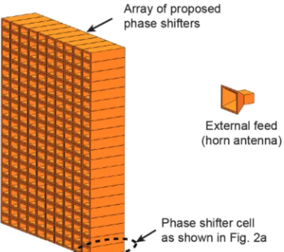
The proposed MEMS-based finline phase shifters are intended to be used as unit-cells to implement a waveguide-based phased array antenna, as shown in Fig. 1, similar to transmit-array antenna concept [32]-[34].
design of the cantilever switches is presented and in Section IV the theoretical phase shifter performance and prototyping of chips to achieve the desired phase states are discussed. An overview of the fabrication process is given in Section V, and the measurement setup and characterization results of prototyped devices are discussed in Section VI. Conclusions are drawn in Section VII.
Fig. 1. Transmit-array based on proposed finline MEMS-based phase shifter elements.
II. C
ONCEPT OFF
INLINEMEMS-
BASEDP
HASES
HIFTER(b)
(c) (d)
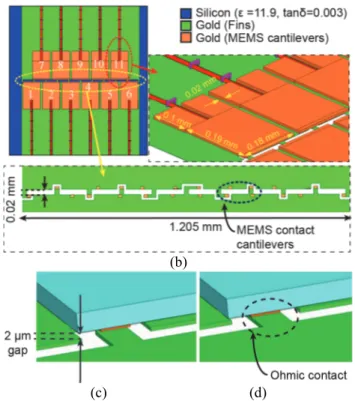
Fig. 2. Finline MEMS-based phase shifter: (a) Schematic view of the finline chip integrated into WR-12 waveguide (3D cross-section view). (b) Side view of one fin with MEMS and comb-like fixed fin slot pattern (ground layer). (c)
Cantilever beam in the open state. (d) Cantilever contact in the closed state.
In finline filters, the metallic finline elements can be placed on one side (unilateral finline) or on both sides of the dielectric substrate (bilateral finline) [35]. A bilateral finline structure integrated along the longitudinal direction of a WR-12 (3.099 mm × 1.549 mm) waveguide made in copper has been used here. The schematic model is represented in Fig. 2, showing the micromachined chip integrated in a waveguide section. The microchips are penetrating through a top and a bottom slot in the waveguide, in order to route the biasing lines of the MEMS cantilevers out of the waveguide. Taking the biasing lines into account is important for any MEMS array device, as the routing of the biasing lines often interferes with RF performance. The phase shifter chips are designed in an X-shape form, as shown in Fig. 2a, which reduces the slot length in the waveguide top and bottom faces, thus keeping the radiation loss and the disturbance of the currents in these waveguide faces at a minimum.
A longitudinal slot (20 µm wide) is patterned in the middle of each fin, as shown in Fig. 2b. 11 MEMS bridges are placed across each fin slot, acting as switches which can short-circuit the slot to influence the wave propagation. In total, this finline phase shifter consists of 22 MEMS cantilever switches. The phase of the wave transmitted from port 1 to port 2 is controlled by a suitable combination of open and closed states of the individual cantilevers. The
distance between the cantilever plate and the electrode is 2.0 µm and 0.8 µm in the “open” and “closed” states, respectively, as shown in Fig. 2c and 2d.
III. MEMS
D
ESIGN ANDM
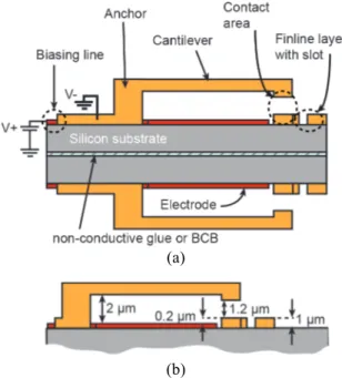
ODELLINGA cross-sectional cut of the proposed cantilever switch mechanism, implemented symmetrically on both sides of the bilateral finline, is shown in Fig. 3. In this design, the majority of the area below the cantilever is used as electrode area to decrease the actuation voltage. The gold layer thickness is designed to 0.8 µm for the electrode pad and to 1.0 µm for the rest of the pattern on the silicon surface, in order to have low metallic losses at the designed frequency of 77 GHz with calculated skin depth of 0.28 µm with a resistivity of 2.44 × 10!!Ω · m and a relative permeability of 1.0 for gold.
For operating the switches, the bottom actuation electrodes are connected to the positive DC voltage through the biasing lines, and the cantilever electrodes are connected to the DC ground, which is shared with the fin layer RF ground. The biasing lines are penetrating the wide walls of the waveguide perpendicular to the length of the chip.
The dimension of the gold cantilever plate is 180.0 µm × 190.0 µm × 6.5 µm (Fig. 2b) and the contact area has a thickness of 0.6 µm (Fig. 3b) which keeps the cantilever at 0.8 µm above the electrode to avoid short circuiting in the down state and which omits the necessity of using any insulating layer. Such a dielectric-less, i.e. all-metal, MEMS switch design eliminates dielectric charging and thus long-term reliability issues. Two separate anchors are used for each cantilever since the biasing lines are routed in the middle of the actuator between these two anchors, as shown is Fig. 2b.
The electro-mechanical design of the cantilever switch is verified by three-dimensional modelling in the finite element method (FEM) software COMSOL Multiphysics. The thickness of the cantilever plate is designed to 6.5 µm, to be deposited by electroplating of gold. The simulated, designed spring constant value is 81.61 N/m assuming an average Young’s modulus of E = 40 GPa and a Poisson’s ratio of ν = 0.42 [36] for electroplated (hard) gold. Such a stiff design results in a high restoring force in the closed state, avoiding switch failure due to gold contact stiction. The simulated actuation (pull-in) voltage is 52.2 V with an electrode pad size of 180.0 µm × 185.0 µm and the simulated resonance frequency of the cantilever beam is 41.54 kHz. This medium actuation voltage for this stiff switch design results in a large contact force and thus stable contact resistance, even for hard gold (cobalt or nickel alloys).
Since a bilateral finline requires symmetrical metal structures, including the reconfigurable MEMS elements, on both sides of the dielectric which is inserted into the waveguide, the chips are designed to be fabricated in two separate, identical parts, each of them comprising 11 MEMS cantilevers on a 300µm-thick (±25µm) silicon substrate, and then to be assembled to a bilateral fin, as shown in Fig. 3.
(a)
(b)
Fig. 3. Cross section view of the cantilever. (a) MEMS actuation and finline fabricated on two different wafers. (b) Component dimensions.
IV. E
LECTROMAGNETICD
ESIGN ANDM
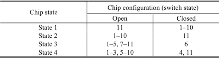
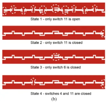
ODELLINGThe proof-of-concept prototypes of the MEMS-based finline phase shifters are designed in fixed MEMS states, i.e. the actuators are not functional, but all actuation and biasing elements are included both in the simulation models and in the fabricated designs, to include their influence on the RF performance. In the fixed state all gold fin layers with all slots for the MEMS biasing lines are patterned (Fig. 2b) but all cantilevers in the closed state are realized with gold short-circuiting connection lines in the slot on the substrate surface. The influence of the contact resistance, typically less than 200 mΩ, is not taken into account in such a simplification. The phase of the transmitted wave is controlled by short-circuiting the slot at specific points which imitates the closed cantilever state of the non-moveable MEMS. Four different embodiments are implemented, which correspond to four different phase states. The cantilever configurations of the four slot configurations are summarized in Table 1. The configuration of cantilever switches for different states shows that four separate actuation signals are required to operate the phase shifter. The
actuation signal 1 needs to be connected to the actuation pads of switches 1-3, 5, and 7-10, and the actuation signals 2, 3, and 4 need to be connected to the actuation pads 4, 6, and 11, respectively.
Table 1 Chip states and their configurations
Chip state Chip configuration (switch state) Open Closed
State 1 11 1–10
State 2 1–10 11
State 3 1–5, 7–11 6 State 4 1–3, 5–10 4, 11
The HFSS simulation model of the finline phase shifter is shown in Fig. 4. HFSS was used for phase-shifter design and optimization, and FEKO was used for design verification. The numerical model consists of a PEC (perfect electric conductor) WR-12 rectangular waveguide (1.55 mm × 3.10 mm × 8.6 mm) with gold-metallized dielectric (silicon, εr=11.9, tanδ=0.003) X-shape inserts placed in the middle of the rectangular waveguide. The
dimensions of the X-shape finline chips are given in Fig. 4a and the layouts of the four slot configurations are shown in Fig. 4b.
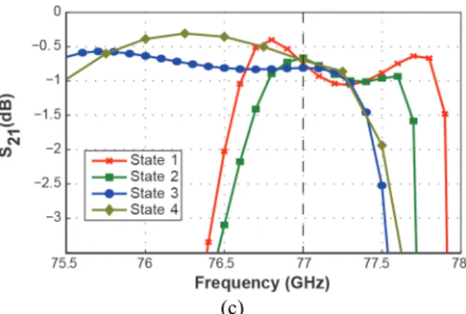
The simulation results of the four states of the MEMS finline phase shifter are shown in Fig. 5. The phase responses of the chips at the nominal design frequency of 77 GHz comprise the following phase states: -113°, -18°, 45° and 133°. The phase values normalized to state 4 are 0°, 95°, 158° and 246°. The simulated reflection coefficient is lower than 10 dB for all states at the design frequency, and the simulated insertion loss S21 is better than -1 dB for
all states at 77 GHz. The states 1 and 2 of this design are very narrowband. Metal and dielectric losses were taken into account in the model.
(b)
Fig. 4. Finline-based phase shifter chip model to check the performance with slots for biasing. (a) The chips are fabricated in X-shape to reduce the opening of the waveguide, thus decreasing the radiation loss while providing the access to the biasing lines. (b) Phase shifter slot configurations for the four different phase shifter states presented in
Table 1.
(a)
(c)
Fig. 5. Simulated results of the finline filter performance designed for 77 GHz using ANSYS HFSS (this design provides a nearly 2-bit resolution): (a) phase response; (b) reflection coefficient; (c) insertion loss.
V. F
ABRICATION OFP
HASES
HIFTERP
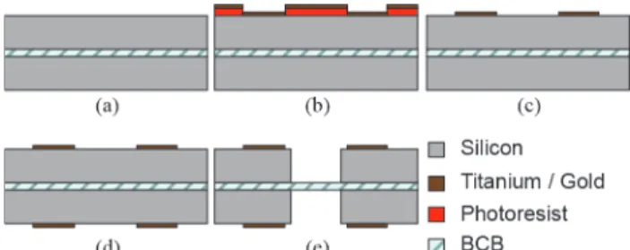
ROTOTYPESThe most important steps of the micromachining process flow of the phase shifters, fabricated on a pair of bonded high resistivity silicon wafers, are shown in Fig. 6. High resistivity silicon substrates (HRSS) with a nominal resistivity of higher than 13000 Ω.cm are used due to low loss tangent of these substrates at room temperature in the entire W-band (75-110 GHz) [37]. After a standard wafer cleaning process, two 300-µm HRSS wafers are bonded using adhesive substrate bonding with benzocyclobutene (BCB) polymer as an intermediate layer (Fig. 6a). Az nLof 2070 negative resist is spin coated and patterned on the front side of the wafer, followed by evaporating of 50 nm titanium adhesion layer and 1 µm layer of gold (Fig. 6b). The sacrificial photoresist is removed in Microposit remover 1165 assisted by ultrasonic agitation to complete the lift-off process (Fig. 6c). The front-side is then protected by a hard-baked 4.5 µm layer of Az 4533 photoresist, followed by repeating the metallization lift-off process on the backside, to achieve a bilateral finline structure (Fig. 6d). Then, two photolithography steps with Az 4533 thick resist are done on both sides of the wafer to pattern the X-shape chip footprints. Then, deep reactive ion etching of the front-side wafer is done in an inductively coupled plasma (ICP) tool. The photoresist mask is stripped in the same tool due to good controllability and to avoid unintentional attacking of the underneath gold layer by ions and radicals of plasma which is harder to control in standard photoresist stripping tools. The processed wafer is attached to a temporary carrier wafer from the front-side by an intermediate thermal-release adhesive tape and deep reactive ion etching is also done on the backside to completely free-etch the chips while they are kept in place on the temporary carrier wafer. The photoresist on the backside is stripped by plasma etching and the chips are released from the thermal-release adhesive tape (Fig. 6e).
The bonding of the wafers before structuring the two finline metallization layers, as compared to fabricating separate chips and then bonding them on chip-level, is that the accuracy of the back-to-bottom-side wafer alignment is by far higher than for chip-to-chip backside alignment, for which no standard fabrication equipment exists. Camera pictures of some prototype microchips are shown in Fig. 7, after being released from the thermal-release adhesive tape.
Fig. 6. Micromachining process flow of phase shifters: (a) bonding with BCB adhesion layer, (b) lithography and evaporate deposition of Ti/Au layer on the front side, (c) lift-off, (d) evaporate deposition of Ti/Au on the backside
followed by lift-off, and (e) DRIE of the front side followed by the backside.
(a) (b)
Fig. 7. Finline-based phase shifter chip prototypes. (a) On the processed wafer after being released from the thermal-release adhesive tape. (b) X-shape chip.
VI. E
XPERIMENTALC
HARACTERIZATION OF THEP
HASES
HIFTERP
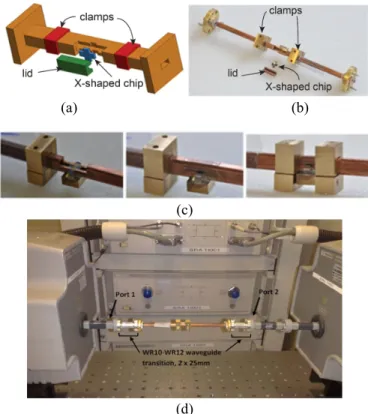
ROTOTYPESIn order to integrate the X-shape phase shifter chips into the measurement setup, a modified 120 mm long WR-12 waveguide section, shown in Fig. 8, is used. A 10 mm long section is cut out of the waveguide. A lid corresponding to that removed section has been fabricated out of a second waveguide. An X-shape recess with slots for the biasing lines has been cut into the original waveguide to guarantee that the chip is positioned exactly in the middle of the waveguide aperture. To keep the chip fixated, the lid is attached and fixated by two sliding clamps (Fig. 8a and 8b). The proposed waveguide structure provides easy and fast access to the chip, i.e. for exchanging the chips for
characterizing different chips. Fig. 8c shows photographs of the X-shape chip integration process into the waveguide. There are three steps: i) inserting the chip into the waveguide recess; ii) closing the lid and fixating all the parts by two clamps; iii) once the clamps are fixated, the measurement can be started. The measurement setup, shown in Fig. 8d, is used to evaluate the finline phase shifter performance experimentally. The two WR-10 waveguide ports of the millimetre-wave heads of a 100 GHz vector network analyser are connected via two adapters to the WR-12 waveguides containing the assembly fixture for mounting the prototype chips.
(a) (b)
(c)
(d)
Fig. 8. Characterization of the performance of X-shape phase shifter chips integrated into tailor-made WR-12 waveguide: (a) WR-12 waveguide model. (b) WR-12 waveguide prototype. (c) Chip fixation into tailor-made WR-12
waveguide section. (d) Measurement setup for chip characterization.
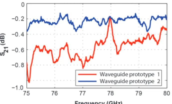
Two prototype waveguides with replaceable sections have been fabricated and characterized. Their insertion loss, with the lid clamped in place, but without any chip inserted is shown in Fig. 9. The insertion loss of this waveguide setup, i.e. the influence of the replaceable caps and of the slots in the top and in the bottom face of the waveguide, is better than 1 dB from 75-80 GHz (normalized by a straight waveguide section of same length, without replaceable cap and slots).
Fig. 9. Measured insertion loss of two prototype waveguides with replaceable sections without the chips being inserted.
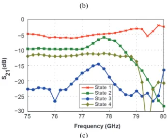
Fig. 10 shows the measured RF performance of the phase-shifter prototype chips inserted in the modified waveguide. The measured phase states (Fig. 10a), relative to state 4, are 0°, 56°, 189°, and 256°, for the design frequency of 77 GHz, which corresponds to an effective 1.78 bit. The measured S-parameters of the four states are shown in Fig. 10b and Fig. 10c. The measured reflection coefficients show that a large amount of power is reflected, much more than expected from the simulations. This can also be seen in the insertion loss which is better than 5.7 dB for the state with the lowest loss.
(b)
(c)
Fig. 10. Measured results of the finline filter performance designed for 77 GHz by ANSYS HFSS: (a) phase response; (b) reflection coefficient; (c) insertion loss.
To investigate the reason for this discrepancy, the reproducibility of the assembly and the influence of fabrication tolerances were investigated. Fig. 11a shows the S21 measurements of 6 different chips fabricated for the same state
(state 2). The deviation between the different chips is not significant and thus fabrication and assembly tolerances are not the reason for the poor RF performance. Furthermore, the reproducibility of the assembly of the chips into the waveguide was investigated. Fig. 11b shows the insertion loss S21 measurements of the same chip (state 4), which is
taken out of the waveguide and re-mounted between subsequent 4 measurements, which shows high consistency. The small deviation of the absolute chip dimensions and the thickness of the bonding polymer interface among different chips were measured and are shown in Fig. 12.
Thus, it is concluded that a major reason for the deviation of the measured S-parameters from the simulation data is the narrow-band design of the devices, which makes the performance very sensitive to design parameter variations.
(b)
Fig. 11. Influence of fabrication tolerances and reproducibility of the assembly: (a) Measured insertion loss of 6 different prototype chips fabricated for state 2, showing insignificant influence of the fabrication tolerances in the vicinity of the designed frequency of 77 GHz. (b) Subsequent measured insertion loss of the same prototype chip fabricated for state 4, which is taken out of the waveguide and remounted between subsequent measurements,
showing reproducibility of the assembly and the measurement.
Fig. 12. Variation of the chip dimensions of different chips.
VII. C
ONCLUSIONIn this paper, we proposed a new configuration of digital phase shifters integrated into WR-12 waveguides. This configuration is based on a finline bandpass filter associated to MEMS elements as switches in fixated states. The phase states are controlled by changing MEMS combination integrated in the finline slot. The nearly 2-bit resolution of the proposed concept is verified both by simulation and measurement. The proposed finline phase shifter was expected to have low insertion loss according to simulations, but the characterized prototype chips, exhibit significantly higher insertion loss. This is not attributed to assembly issues or fabrication tolerances, which are
investigated in the paper, but most likely to the narrow-band design and thus the high sensitivity to design parameter variations.
VIII. A
CKNOWLEDGMENTThe research leading to these results has received funding from the European Community's Seventh Framework Programme (FP7/2007-2013) under grant agreement no. 224197 and was carried out in the frame of TUMESA project (MEMS Tuneable Metamaterials for Smart Wireless Applications, 2008-2011).
IX.
R
EFERENCES[1] Brown, E.R.: ‘RF-MEMS switches for reconfigurable integrated circuits’, IEEE Trans. Microw. Theory Tech., 1998, 46, (11), pp. 1868–1880
[2] Barker, N.S., and Rebeiz, G.M.: ‘Optimization of distributed MEMS transmission-line phase shifters-U-band and W-band designs’, IEEE Trans. Microw. Theory Tech., 2000, 48, (11), pp. 1957–1966
[3] Hung, J.-J., Dussopt, L., and Rebeiz, G.M.: ‘Distributed 2- and 3-bit W-band MEMS phase shifters on glass substrates’, IEEE Trans. Microw. Theory Tech., 2004, 52, (2), pp. 600–606
[4] Stehle, A., Georgiev, G., Ziegler, V., Schoenlinner, B., Pretchel, U., Seidel, H., and Schmid, U.: ‘RF-MEMS switch and phase shifter optimized for W-band’. Proc. 38th European Microwave Conference, Amsterdam,
Netherlands, Oct 2008, pp. 104–107
[5] Rizk, J.B., and Rebeiz, G.M.: ‘W-band CPW RF MEMS circuits on quartz substrates’, IEEE Trans. Microw. Theory Tech., 2003, 51, (7), pp. 1857–1862
[6] Rizk, J.B., and Rebeiz, G.M.: ‘W-band microstrip RF-MEMS switches and phase shifters’. IEEE MTT-S International Microwave Symposium Digest, Philadelphia (Pennsylvania), USA, June 2003, pp. 1485–1488 [7] Lucyszyn, S.: ‘Review of radio frequency microelectromechanical systems technology’, IEE Proceedings
Science, Measurement and Technology, March 2004, 151, (2), pp. 93–103
[8] Ulm, M., Schobel, J., Reimann, M., Buck, T., Dechow, J., Muller-Fiedler, R., Trah, H.-P., and Kasper, E.: ‘Millimeter-wave microelectromechanical (MEMS) switches for automotive surround sensing systems’. 2003 Topical Meeting on Silicon Monolithic Integrated Circuits in RF Systems, Grainau, Germany, April 2003, pp. 142–149
[9] Sterner, M., Chicherin, D., Raisenen, A.V., Stemme, G., and Oberhammer, J.: ‘RF MEMS high-impedance tuneable metamaterials for millimeter-wave beam steering’. IEEE 22nd International Conference on Micro
Electro Mechanical Systems, Sorrento, Italy, Jan 2009, pp. 896–899
[10] Schoebel, J., Buck, T., Reimann, M., Ulm, M., Schneider, M., Jourdain, A., Carchon, G.J., and Tilmans, H.A.C.: ‘Design considerations and technology assessment of phased-array antenna systems with RF MEMS for automotive radar applications’, IEEE Trans. Microw. Theory Tech, 2005, 53, (6), pp. 1968–1975
[11] Caekenberghe, K. Van: ‘RF MEMS technology for radar sensors’. International Radar Conference - Surveillance for a Safer World, Bordeaux, France, Oct. 2009, pp. 1–6
[12] Rebeiz, G.M.: ‘RF MEMS theory, design, and technology’, (Wiley, New Jersy, 2003, 1st ed.)
[13] Varadan, V.K., Vinoy, K.J., and Jose, K.A.: ‘RF MEMS and Their Applications’, (Wiley, Chichester, UK, 2003, 1st ed.)
[14] Scardelletti, M.C., Ponchak, G.E., Zaman, A.J., and Lee, R.Q.: ‘RF MEMS phase shifters and their application in phase array antennas’. Proc. IEEE Annu. Wireless Microw. Technol. Conf., Clearwater Beach (FL), USA, 2005, pp. 191–194
[15] Boyd, C.R.: ‘A 60 GHz Dual-Mode Ferrite Phase Shifter’. IEEE MTT-S International Microwave Symposium Digest, Dallas (TX), USA, June 1982, pp. 257–259
[16] Higgins, J.A., Hao Xin, Sailer, A., and Rosker, M.: ‘Ka-band waveguide phase shifter using tunable electromagnetic crystal sidewalls’, IEEE Trans. Microw. Theory Tech., 2003, 51, (4), pp. 1281–1288
[17] Popov, M.A., Zavislyak, I.V., and Srinivasan, G.: ‘Magnetic field tunable 75-110 GHz dielectric phase shifter’, IET Electron. Lett., 2010, 46, (8), pp. 569–570
[18] Mueller, S., Goelden, F., Scheele, P., Wittek, M., Hock, C., and Jakoby, R.: ‘Passive Phase Shifter for W-Band Applications using Liquid Crystals’. Proc. 36th European Microwave Conference, Manchester, UK, 2006, pp. 306–309
[19] Lakshminarayanan, B., and Weller, T. M.: ‘Optimization and implementation of impedance-matched true-time-delay phase shifters on quartz substrate’, IEEE Trans. Microw. Theory Tech., 2007, 55, (2), pp. 335–342 [20] McFeetors, G., and Okoniewski, M.: ‘Distributed MEMS analog phase shifter with enhanced tuning’, IEEE
[21] Somjit, N., Stemme, G., and Oberhammer, J.: ‘Binary-coded 4.25-bit W -band monocrystalline–silicon MEMS multistage dielectric-block phase shifters’, IEEE Trans. Microw. Theory Tech., 2009, 57, (11), pp. 2834–2840 [22] Psychogiou, D., Li, Y., Hesselbarth, J., Peroulis, D., Hierold, C., and Hafner, C.: ‘Continuously variable
W-band phase shifters based on MEMS-actuated conductive fingers’, International Journal of Microwave and Wireless Technologies, Apr 2013 (Published online)
[23] Arndt, F., Bornemann, J., and Grauerholz, D.: ‘Theory and design of low-insertion loss fin-line filters’, IEEE Trans. Microwave. Theory Tech., 1982, 30, (2), pp. 155–163
[24] Button, K.J.: ‘Topics in millimeter wave technology’ (New York: Academic Press Inc, 1988), Chap 1
[25] Fu, J.S.: ‘Development of mm-wave source in finline structure for high speed digital communications’. Proc-Asia Pacific Seminar on Next Generation Mobile Communication System, Jan 2000, pp. 1–17
[26] Daneshmand, M., Mansour, R., and Sarkar, N.: ‘RF MEMS waveguide switch’, IEEE Trans. Microwave Theory Tech., 2004, 52, (12), pp. 2651–2657
[27] Daneshmand, M., and Mansour, R.: ‘Multiport MEMS-based waveguide and coaxial switches,” IEEE Trans. Microwave Theory Tech., 2005, 53, (11), pp. 3531–3537
[28] Pelliccia, L., Farinelli, P., and Sorrentino, R.: ‘MEMS-based high-Q reconfigurable E-plane filters’. Proc. IEEE European Microw. Conf. (EuMC), Manchester, UK, Oct. 2011, pp. 369–372
[29] Liu, X., Katehi, L.P.B., Chappell, W., and Peroulis, D.: ‘High-Q tunable microwave cavity resonators and filters using SOI-based RF MEMS tuners’, J. Microelectromech. Syst., 2010, 19, (4), pp. 774–784
[30] Sterner, M., Chicherin, D., Raisenen, A.V., Stemme, G., Oberhammer, J.: ‘RF MEMS high-impedance tuneable metamaterials for millimeter-wave beam steering’. IEEE 22nd International Conference on Micro Electro Mechanical Systems (MEMS), Sorrento, Italy, 25-29 Jan. 2009, pp. 896–899
[31] Baghchehsaraei, Z., Shah, U., Dudorov, S., Stemme, G., Oberhammer, J., Åberg, J.: ‘MEMS 30µm-thick W-band waveguide switch’, 42nd European Microwave Conference (EuMC), Amsterdam, Netherlands, Oct.29 2012-Nov.1 2012, pp. 1055–1058
[32] Boccia, L., Russo, I., Amendola, G., and Di Massa, G.: ‘Multilayer antenna-filter antenna for beam-steering transmit-array applications’, IEEE Trans. Microw. Theory Tech., 2012, 60, (7), pp. 2287–2300
[33] Kaouach, H., Dussopt, L., Lantéri, J., Koleck, Th., and, Sauleau, R.: ‘Wideband low-loss linear and circular polarization transmit-arrays in V-band’, IEEE Trans. Antennas Propagat., 2011, 59, (7), pp. 2513–2523
[34] Clemente, A., Dussopt, L., Sauleau, R., Potier, P., and Pouliguen, Ph.: ‘1-bit reconfigurable unit-cell based on PIN diodes for transmit-array applications in X-band’, IEEE Trans. Antennas Propagat., 2012, 60, (5), pp. 2260–2269
[35] Bhat, B., and Koul, S.K.: ‘Analysis design and applications of fin lines’ (Artech House, 1987), Chap 9
[36] Baek, C.W., Kim, Y.K., Ahn, Y., Kim, Y.H.: ‘Measurement of the mechanical properties of electroplated gold thin films using micromachined beam structures’. Sensors and Actuators a-Physical, 2005, 117, (1), pp. 17-27 [37] Afsar, M.N., and Chi, H.: ‘Millimeter wave complex refractive index, complex dielectric permittivity and loss
tangent of extra high purity and compensated silicon’, Int. J. of Infrared and Millimeter Waves, 1994, 15, (7), pp. 1181–1188