HAL Id: hal-01136443
https://hal.archives-ouvertes.fr/hal-01136443
Submitted on 27 Mar 2015
HAL is a multi-disciplinary open access
archive for the deposit and dissemination of sci-entific research documents, whether they are pub-lished or not. The documents may come from teaching and research institutions in France or abroad, or from public or private research centers.
L’archive ouverte pluridisciplinaire HAL, est destinée au dépôt et à la diffusion de documents scientifiques de niveau recherche, publiés ou non, émanant des établissements d’enseignement et de recherche français ou étrangers, des laboratoires publics ou privés.
Phase-sensitive optical processing in silicon waveguides
K Petermann, A Gajda, G Dziallas, M Jazayerifar, L Zimmermann, B Tillack,
F da Ros, D Vukovic, K Dalgaard, M Galili, et al.
To cite this version:
K Petermann, A Gajda, G Dziallas, M Jazayerifar, L Zimmermann, et al.. Phase-sensitive optical processing in silicon waveguides. Optical Fiber Communication Conference (OFC 2015), Mar 2015, Los Angeles, United States. pp.Tu2F.4, �10.1364/OFC.2015.Tu2F.4�. �hal-01136443�
Tu2F.4.pdf OFC 2015 © OSA 2015
Phase-sensitive optical processing in silicon waveguides
K. Petermann1, A. Gajda1, G. Dziallas1, M. Jazayerifar1, L. Zimmermann2, B. Tillack2 F. Da Ros3, D. Vukovic3, K. Dalgaard3, M. Galili3, C. Peucheret4
(1) Technische Universität Berlin, HFT4, Einsteinufer 25, 10587 Berlin, Germany
(2) IHP, Im Technologiepark 25, 15236 Frankfurt (Oder), Germany
(3) Technical University of Denmark, Department of Photonics Engineering, DK-2800 Kgs. Lyngby, Denmark
(4) University of Rennes 1, FOTON Laboratory, CNRS UMR 6082, ENSSAT, F-22305 Lannion, France Abstract: Parametric optical signal processing is reviewed for silicon nano-rib-waveguides with a
reverse-biased pin-junction. Phase-sensitive parametric amplification with a phase-sensitive extinction of more than 20 dB has been utilized for the regeneration of DPSK signals.
OCIS codes: (130.3120) Integrated optics devices; (190.4360) Nonlinear optics devices; (190.4975) Parametric processes;
(230.7405) Wavelength conversion devices
1. Introduction
The use of parametric processes using the 3rd order optical nonlinearity in optical materials for applications such as low noise amplification, wavelength conversion, signal regeneration and other kinds of optical signal processing has raised considerable interest over the last years [1-3]. In particular, parametric processes also allow for phase-sensitive optical amplification, which may be utilized for signal regeneration [4], even for higher order modulation formats [5]. Most experiments have so far been conducted using highly nonlinear silica fibers (HNLFs), which require a length of typically several hundred meters due to the relatively low optical nonlinearity in silica.
In order to achieve compact modules, 3rd order nonlinearities may also be utilized in photonic integrated circuits (PICs). For this purpose, PICs have been either based on glasses or semiconductor materials. With respect to PICs based on glass materials, nonlinear parametric processing has been demonstrated, e.g. for silicon nitride, Hydex [6] or chalcogenide glasses [7]. Even though the nonlinearities in these waveguides are about two orders of magnitude higher than in silica-HNLFs, they usually still require pump powers in excess of several Watts because of the relatively short interaction lengths in PICs. Nevertheless, it has been possible to achieve a phase-sensitive extinction ratio of around 10 dB in a dual-pump degenerate-idler configuration with planar chalcogenide glass waveguides [8] in pulsed operation.
Much higher nonlinearities are feasible in PICs based on semiconductor materials, where silicon is of particular interest [9]. It combines the advantage of a relatively high 3rd order nonlinearity with the realization of nanowires with tiny effective cross sections down to about 0.1 µm2 exhibiting nonlinear phase shifts of around 200…300 rad/(W·m), which is about 4 orders of magnitude higher than in silica HNLFs. Even higher effective nonlinearities are possible for photonic crystal Si-nano-waveguides thanks to slow light enhancement, where, for a phase-sensitive amplifier in pulsed operation, a phase-sensitive extinction ratio of 11 dB has been achieved [10].
However, silicon suffers from two-photon-absorption (TPA) and the associated generation of carriers leading to free-carrier absorption (FCA). TPA can be reduced using amorphous instead of crystalline silicon [11] or silicon-slot waveguides employing polymers on a silicon-organic platform [12]. However, both concepts suffer from relatively high linear losses and a limited compatibility with CMOS or BiCMOS micro-electronics. TPA can also be omitted by operating the devices at longer infrared wavelengths [13,14]. The influence of FCA can be reduced for operation with pulsed pump sources, which is, however, not adequate for telecom applications. Alternatively, FCA in crystalline silicon nano-waveguides can be considerably reduced by reducing the effective carrier lifetime down to about 10-20 ps via a reverse biased pin-junction [15-17].
In this paper, we review our recent achievements on the design and fabrication of silicon nanowires using reverse-biased pin junctions and their applications for phase-sensitive all-optical signal processing at telecom wavelengths using cw-pump sources.
2. Silicon nano-waveguide design
(a) (b)
Tu2F.4.pdf OFC 2015 © OSA 2015
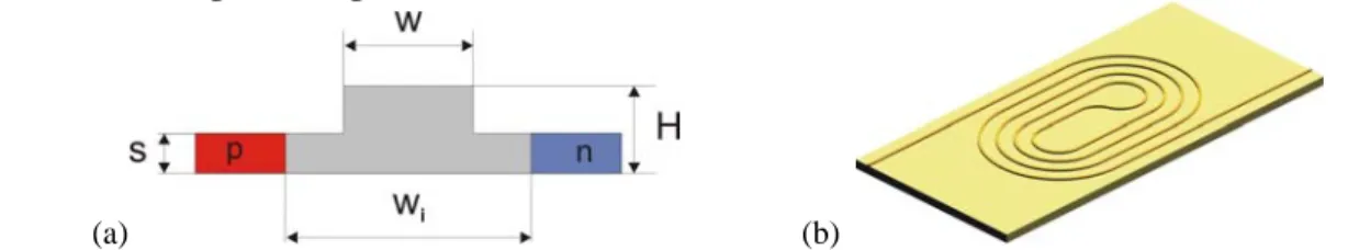
In order to combine Si-nano-waveguides with a pin-junction, nano rib-waveguides have been fabricated according to Fig. 1 on 2 µm thick buried oxide with W=500 nm, H=210 nm, s=50 nm and wi=1200 nm within the
BiCMOS foundry of IHP using a 248 nm lithography with a linear loss of about 1 dB/cm [18]. The waveguide is realized in form of a spiral yielding a small footprint of only 2.5 × 0.6 mm2
for a waveguide with a length of 4 cm.
3. Wavelength conversion with four-wave mixing
Si rib waveguides with a reverse biased pin-junction allow for very efficient wavelength conversion via four-wave mixing [15,18,19]. As shown in Fig. 2, a record cw conversion efficiency (defined as the ratio between idler and signal power at the waveguide output) of -1 dB has been achieved (best value of -0.7 dB) [18].
Fig. 2. Schematic of wavelength conversion within a Si-nano-waveguide with grating input/output-couplers and measurement results (length of the waveguide L=4cm, loss per grating coupler ~ 4.5 dB, cw-pump power before the grating 26 dBm, reverse bias voltage 20 V) [18].
This high conversion efficiency was achieved for just 26 dBm of external cw-pump power, corresponding to a pump power inside the waveguide of only about 150 mW. The conversion bandwidth is limited by the relatively high amount of chromatic dispersion, which we estimate to about -2.5 ps/(m·nm) for our specific waveguide [20,21]. These results underline the high efficiency of four-wave mixing processes in Si nano-waveguides, which have also been exploited for error-free wavelength conversion of 40 Gbit/s on-off keying (OOK) modulated signals [21].
4. Phase-sensitive optical signal processing
Based on the high efficiency of four-wave mixing processes in silicon waveguides, it is also very attractive to study phase-sensitive parametric processing in these waveguides with the purpose of signal regeneration of phase modulated signals. We did investigate both phase-sensitive parametric gain as well as the regeneration of 10 Gbit/s differential phase-shift keying (DPSK) signals [22, 23] with a set-up as shown in Fig.3.
ECL PM OBPF 40 GHz Feedback loop PC OBPF EDFA APD 10 dB SSMF Optical Processor EDFA
Freq. Comb Generator
Phase stabilization feedback
DC BIAS Si WAVEGUIDE PM Noise emulation PZT Bit Pattern Generator OBPF Pre-amplified Balanced Receiver pumps signal MZM
Fig. 3 Experimental set-up for the dynamic phase regeneration of a 10 Gbit/s DPSK-signal [23].
A frequency comb is being synthesized with a phase-modulator (PM) with a 40 GHz sinusoidal drive signal. The optical processor selects three neighboring comb lines. The two outer comb lines act as phase synchronized pumps and the central line serves as the signal. Fig. 4a shows the measured signal power at the output of the waveguide as a function of the signal phase. For a total cw-pump power PT of 24 dBm before the grating (corresponding to ~50 mW
per pump inside the waveguide) and a reverse bias of 20 V, one obtains a phase-sensitive extinction ratio of 11 dB, which can be improved by increasing the pump power to PT=28 dBm ( ~110 mW per pump inside the waveguide)
and by increasing the reverse bias voltage to 25 V (for reducing the effective carrier lifetime) to a record extinction ratio up to 20 dB [23]. This phase-sensitive gain has been used for the regeneration of 10 Gbit/s DPSK signals. As shown in Fig. 3, the DPSK signal is first generated with a Mach-Zehnder modulator (MZM) and is subsequently
Tu2F.4.pdf OFC 2015 © OSA 2015
distorted by a harmonically driven (f=5 GHz) phase modulator. Excellent regeneration results have been obtained for a cw-pump power of 24 dBm and a reverse bias voltage of 25 V, as shown in Fig. 4b.
0 50 100 150 200 250 -20 -18 -16 -14 -12 -10 -8 -6 -4 -2 0 normalized power (dB)
signal phase (deg)
PT= 24 dBm 20 V PT= 25 dBm 20 V PT= 26 dBm 20 V PT= 27 dBm 20 V PT= 28 dBm 20 V PT= 28 dBm 25 V
a)
-45 -40 -35 -30 -25 12 11 10 9 8 7 6 5 4 3 2 input outputw/o phase noise w/ phase noise
-log(B
ER
)
average received power (dBm)
input output w/o noi se w/ n oise b)
Fig. 4. Phase-sensitive output power (a) and BER curves for a regenerated 10 Gbit/s DPSK signal (b) [23]
5. Conclusion
Nano-rib-waveguides with a reverse biased pin-junction are very suitable for advanced parametric signal processing with relatively low cw-pump powers in the order of 100 mW despite the existence of TPA in silicon at telecommunications wavelengths. Further improvement is expected by suitably tailoring the chromatic dispersion and further reducing the linear losses in the nano-rib-waveguides.
Acknowledgement
This work was partly funded by the German Research Foundation (DFG) in the framework of the Sonderforschungsbereich SFB787 and by the Danish Research Council for Technology and Production Sciences (project 09-066562). Financial support from Villum Fonden via the NATEC Centre is acknowledged.
References
[1] J. Hansryd et al., “Fiber-based optical parametric amplifiers and their applications,” IEEE J. Sel. Top. Quantum Electron. 8, 506-520 (2002). [2] Z. Tong, S.Radic, “Low-noise optical amplification and signal processing in parametric devices,” Adv. Opt. Photon. 5, 318-384 (2013). [3] M.E. Marhic, Fiber optical parametric amplifiers, oscillators and related devices (Cambridge University Press, 2007)
[4] R Slavík et al., “All-optical phase and amplitude regenerator for next-generation telecommunications systems,” Nature Photon. 4, 690-695 (2010)
[5] T. Richter et al., “QAM Phase regeneration in a phase-sensitive fiber-amplifier,” in Proc. ECOC 2013 (IEE, London, 2013), We.3.A.2 [6] D.J. Moss et al., “New CMOS-compatible platforms based on silicon nitride and Hydex for nonlinear optics,” Nature Photon. 7, 597-607 (2013).
[7] B.J. Eggleton et al., “Chalcogenide photonics,” Nature Photon. 5, 141-148 (2010).
[8] R. Neo et al., “Phase-sensitive amplification of light in a chi(3) photonic chip using a dispersion engineered chalcogenide ridge waveguide,” Opt. Express 21, 7926-7933 (2013).
[9] J. Leuthold et al., “Nonlinear silicon photonics,” Nature Photon. 4, 535-544 (2010).
[10] Y. Zhang et al., “Phase sensitive amplification in silicon photonic crystal waveguides,” Opt. Letters 39, 363-366 (2014).
[11] C. Grillet et al., “Amorphous silicon nanowires combining high nonlinearity, FOM and optical stability,” Opt. Express 20, 22609-22615 (2012).
[12] C. Koos et al., “All-optical high-speed signal processing with silicon-organic hybrid slot waveguides,” Nature Photon. 3, 216-219 (2009). [13] X. Liu et al., “Mid-infrared optical parametric amplifier using silicon nanophotonic waveguides,” Nature Photon. 4, 557-560 (2010). [14] B. Kuyken et al., “50 dB parametric on-chip gain in silicon photonic wires,” Opt. Letters 36, 4401-4403 (2011).
[15] W. Mathlouthi et al., “Characterization of efficient wavelength conversion by four-wave mixing in sub-micron silicon waveguides,” Opt. Express 16, 16735–16745 (2008).
[16] A.C. Turner-Foster et al., “Ultrashort free-carrier lifetime in low-loss silicon nanowaveguides,” Opt. Express 18, 3582-3591 (2010). [17] A. Gajda et al., “Design rules for p-i-n diode carriers sweeping in nano-rib waveguides on SOI,” Opt. Express 19, 9915-9922 (2011). [18] A. Gajda et al., “Highly efficient CW parametric conversion at 1550 nm in SOI waveguides by reverse biased p-i-n junction,” Opt. Express
20, 13100–13107 (2012).
[19] J. R. Ong et al.,” Efficient CW four-wave mixing in SOI micro-rings with active carrier removal”, IEEE Photon. Technol. Lett. 25, 1699-1701 (2013)
[20] G. Dziallas et al., “A numerical investigation of continuous wave parametric gain in silicon nano-waveguides at wavelengths around 1550 nm,” in Proceedings NUSOD 2014, paper TuB3, Palma de Mallorca, Spain, 2014.
[21] A. Gajda et al., “High efficiency wavelength conversion of 40 Gbps signals at 1550 nm in SOI nano-rib waveguides using p-i-n diodes,” IEEE Int. Conf. Group IV Photonics, paper FC3, Seoul, Korea, 2013.
[22] F. Da Ros et al., “Continuous wave phase-sensitive four-wave mixing in silicon waveguides with reverse-biased p-i-n junctions,” in Proc. ECOC 2013 (IEE, London, 2013), P.2.11
[23] F. Da Ros et al., “Phase regeneration of DPSK signals in a silicon waveguide with reverse-biased p-i-n junction,” Opt. Express 22, 5029-5036 (2014).
![Fig. 3 Experimental set-up for the dynamic phase regeneration of a 10 Gbit/s DPSK-signal [23]](https://thumb-eu.123doks.com/thumbv2/123doknet/12278176.322235/3.918.139.808.704.867/fig-experimental-dynamic-phase-regeneration-gbit-dpsk-signal.webp)
