This is an author-deposited version published in:
http://oatao.univ-toulouse.fr/
Eprints ID: 11333
To link to this article: DOI: 10.1111/ijac.12213
URL:
http://dx.doi.org/10.1111/ijac.12213
To cite this version:
Debéda, Hélène and Lucat, Claude and Maglione,
Mario and Pommier-Budinger, Valérie and Hochart, Xavier and Sourbe,
Wilfrid Feasibility of Screen-Printed PZT Microceramics for Structural
Health Monitoring Applications. (2014) International Journal of Applied
Ceramic Technology . ISSN 1744-7402
O
pen
A
rchive
T
oulouse
A
rchive
O
uverte (
OATAO
)
OATAO is an open access repository that collects the work of Toulouse researchers and
makes it freely available over the web where possible.
Any correspondence concerning this service should be sent to the repository
administrator:
staff-oatao@inp-toulouse.fr
Feasibility of Screen-Printed PZT Microceramics for Structural
Health Monitoring Applications
H!el"ene Deb!eda* and Claude Lucat
Universit!e de Bordeaux, IMS, UMR 5218, Talence F-33400, France
Mario Maglione
CNRS, ICMCB, UPR 9048, Pessac F-33600, France
Val!erie Pommier-Budinger
Universit!e de Toulouse, Institut Sup!erieur de l’A!eronautique et de l’Espace, Toulouse F-31055, France
Xavier Hochart
TEMEX-Ceramics, Parc industriel Bersol, Pessac F-33600, France
Wilfrid Sourbe
RESCOLL, Soci!et!e de Recherche, CS30021, Pessac F-33615, France
Using the association of low-cost screen-printing technology with the sacrificial layer method, the feasibility of totally released piezoelectric thick-film microceramics of gold-electroded PZT type is studied. After the deposition of the sacrificial layer on an alumina substrate and subsequent printing and drying of gold/PZT/gold layers, the final firing is performed at low temper-ature. This is followed by the releasing step of the Au/PZT/Au in a diluted acidic solution. Impedance analysis shows that the electrical properties and electromechanical coefficients of poled PZT thick films are still lower than those of PZT ceramics. This result is correlated with the high porosity rate of the PZT layer. However, these piezoelectric microceramics present desirable electromechanical behavior and can therefore be used as dynamic-mode sensors or as actuators to generate vibrations in a struc-ture on which they are bonded. Moreover, the successful fabrication and the electromechanical impedance (EMI) levels obtained on a metallic structure suggest possible structural health monitoring applications of these screen-printed PZT microceramics.
Introduction
Compared to traditional time-consuming and expensive nondestructive evaluation techniques based on ultrasonic scan, passive thermography, X radiography, etc., structural health monitoring (SHM) appears to be an attractive tool for damage detection (including loca-tion) in degraded composite structures.1 Such a system not only can reduce maintenance costs but also improve safety and reliability. Among various types of transduc-ers, piezoelectric materials are used for SHM because they can be used as either actuators or sensors due to the piezoelectric effect. For this purpose, cost-effective piezo-electric systems can be used within a network of suitably integrated and arranged transducers for real-time
moni-toring and prediction of damage.2 In the active/sensing mode, both Lamb-wave-propagation-based and electro-mechanical impedance (EMI)-based materials have been developed as monitoring methods.3 The EMI method, chosen in this study, involves exciting the structure with a piezoelectric transducer and simultaneously measuring the current generated in the same piezoelectric transducer shunted on a resistor. The current is a result of the elec-tromechanical coupling between the structure and the piezoelectric transducer and consequently provides infor-mation related to the structure’s mechanical impedance. This signal therefore varies when damage occurs and induces changes in the structural impedance. As for the Lamb-wave method, variations between a reference and a damaged structure enable damage to be detected, includ-ing its location.4
Among piezoelectric materials, PZT is often pre-ferred because of its higher sensing/actuating properties.5 *helene.debeda@ims-bordeaux.fr
In case of SHM applications, thin PZT ceramics can, for example, be bonded onto the surface of the structure or embedded into the structure itself to permit the determi-nation of local values of strains. Nevertheless, because piezoelectric ceramic components are poorly adapted to curved surfaces, they are often replaced by more flexible piezoelectric composites. These components are made of piezoelectric microceramics or fibers embedded in a resin.6 The brittleness, sensor fracture, and subsequent degradation of mechanical/electrical properties are the most common types of failures of these embedded thin piezoelectric microceramics. Generally, thin piezoelectric ceramics are fabricated from bulk ceramic as discrete components with specific dimensions. This manufactur-ing process implies some restrictions to the minimum dimension of the microceramic (thickness >100 lm) and often limits their geometry to simple shapes like disks, rectangular plates, rings, etc. Another possibility is to use thin-film technology which is more concerned with sam-ples of low thickness (<1 lm). Therefore, to span the gap between the bulk and the thin-film technologies (1–110 lm), screen-printed PZT thick films seem to be promising candidates.7,8 Moreover, screen-printing tech-nology is known to be a reliable and low-cost process for miniaturization of components and has already been suc-cessfully used for different piezoelectric applications.9–15
In this work, using the association of the screen-printing technology with the sacrificial layer method, we study the feasibility of totally removed gold-electroded PZT thick films (Au/PZT/Au). These can be embedded in a resin to realize piezocomposites for SHM applica-tions. For this purpose, we prepare microceramics based on a mixture of a PZT powder with a eutectic composi-tion allowing for a low sintering temperature (900°C) while maintaining desirable piezoelectric properties. Then, thanks to SEM and microprobe analyses, densifi-cation and composition of the active PZT layer is stud-ied and compared with those of bulk ceramic processed under the same conditions. Electrical and electromechan-ical characterizations are also achieved. Finally, we inves-tigate the sensing, actuating, and EMI behaviors of piezoelectric thick-films components clamped on a metallic beam structure to evaluate their potential for SHM applications.
Processing of Disk-Shaped Au/PZT/Au Microceramics Free- Standing Component Processing
The combination of screen-printing technology and the sacrificial layer method has already been successfully applied for the fabrication of bridge-type or cantilever
piezoelectric microsystems Au/PZT/Au, partially released from an alumina substrate after removal of sacrificial layer.16 The microceramics are composed of a PZT layer between two gold electrodes (Fig. 1). The gold ink is commercially available (ESL8836 from ElectroScience Laboratories, ESL Europe, Berkshire, UK), whereas the sacrificial layer and PZT inks are prepared at the IMS laboratory. The sacrificial layer paste is a mixture of 60 wt% epoxy CV59 (ElectroScience Laboratories) and 40 wt% strontium carbonate (SrCO3, Carlo Erba),
tak-ing into account its printability. The piezoelectric paste is prepared from a commercial piezoelectric PZT powder (PZ26 from Ferroperm, Helsingor, Denmark) mixed with 3 wt% LBCu (25 wt% Li2CO3, 40 wt% Bi2O3,
35 wt% CuO), blended with the organic vehicle ESL400 (ElectroScience Laboratories). The sacrificial layer, bot-tom electrode, piezoelectric layer, and top electrode are printed successively, including a drying step of 20 min
(a)
(b)
Fig. 1. (a) Piezoelectric Au/PZT/Au bridge fabrication: screen-printing process with the sacrificial layer method. (b) Scheme and photograph of screen-printed piezoelectric Au/PZT/Au bridge (2.5 9 2.5 9 0.08 mm3).
at 120°C between each deposition. Subsequently, the samples are dried and isostatically pressed 1 mn at 103MPa to improve the densification.17 Afterward, the samples are co-fired 2 hours at 900°C in air before the removal of the sacrificial layer in a phosphoric acid aque-ous solution. Finally, the microceramics are poled at a temperature Tpoling= 270°C during 5 min, at a
maxi-mum electric field of 50 kV/cm under dry nitrogen. This poling temperature is just below the Curie tempera-ture (Tc ~280°C). We checked the transition
tempera-ture of our samples using real and imaginary part of the admittance versus temperature G(T) and B(T). Being proportional to the capacitance, it is the B(T) curve which gives the best evidence for the transition tempera-ture.18 By using a Sawyer-Tower circuit, a remanent polarization of 2.5 lC/cm² and a coercive field of 30 KV/cm are measured.
Totally Released Disk-Shaped Microceramics Processing
Concerning our SHM application, the process described above has been applied for the fabrication of dis-crete Au/PZT/Au microceramics which must be totally released from the substrate. The PZT composition (97 wt % PZ26 + 3 wt%LBCu) and the three pastes used during this fabrication are identical as those prepared previously. The components are made of PZT and Au electrodes of 10 and 9 mm diameter, respectively (Fig. 2).
The screen-printed sacrificial layer (50 lm) entirely covers the 2.5 9 2.5 cm2alumina substrate. After print-ing, the dried thicknesses of gold and PZT layers are 5 and 200 lm, respectively. The 3-D profiles of the differ-ent printed layers, realized on four microceramics with an optical profilometer (Altisurf 500) before firing, shows good process reproducibility (Fig. 3).
To optimize the sintering process, TGA/DSC analyses have been performed on the PZT ink under O2at 1°C/
min (Fig. 4). The temperatures of organic binder elimina-tion (30 < T(°C) < 350), carbonate decomposition (450 <T(°C) < 650), LBCu eutectic fusion (T ~600°C),
and PbO evaporation (T ~920°C) are observed. Taking into account these results, the temperature profile is opti-mized to prevent cracks and deformations while maximum densification of multilayer PZT microceramics is desired. Heating rates of 1°C/min up to 400°C and 20°C/min up to 900°C are chosen, respectively, for a slow elimination of the organic binder followed by the strontium carbonate decomposition and the onset of liquid-phase sintering at higher temperature. Finally, the samples are sintered 2 hours at 900°C under dry air and cooled down to room temperature at 20°C/min. After the thermal treatment, the multilayer ceramic disk exhibits a flat geometry (Fig. 5).
Characterizations of the Au/PZT/Au Microceramics Microstructure and Physicochemical Characterizations
X rays and quantitative microprobe analysis confirm the tetragonal crystallographic structure of PbZr0.52Ti0.48O3
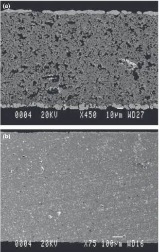
type of the commercial PZ26 material. SEM analyses performed on released PZT thick films illustrate a higher residual porosity than those of pellets made with the same powder (PZ26 + 3%LBCu), pressed at 11 MPa, and fired with the same temperature profile (2 h at 900°C) (Fig. 6).
Fig. 2. Multilayer structure of the Au/PZT/Au disk component before the co-firing.
Fig. 3. 3-D thickness profiles of dried sacrificial layers Au/PZT/ Au on alumina substrate.
Fig. 4. TGA/DSC measurements performed on a PZT + LBCu ink at 1°C/min under dry O2.
The estimated density qPZT ~5.2 g/cm3 for the
screen-printed PZT microstructure, lower than that of the pellet qPZT~7.2 g/cm3of the same composition and
fired in the same way, is much lower than that of the PZT commercial ceramics qPZT ~7.7 g/cm3. The lower
lateral shrinkage measured for PZT electroded thick-film (5%) compared to that of the pellet (13%) confirms these results. The contact of the bottom gold electrode and of the edge of the PZT thick-film against the SrCO3
sacrificial layer during the firing process may explain the slowing down of the shrinkage process.
Interactions between the sacrificial layer and the upper layers are confirmed by microprobe analyses (CAMECA SX 100) performed at the interface between the bottom Au electrode and the PZT thick-film (Table I). Diffusions of PZT in the Au electrode and of Cu at the interface are observed. Moreover, traces of Sr are located in the bottom Au layer.
Electromechanical Characterizations
Electromechanical analysis of Au/PZT/Au disk is per-formed with an impedance analyser HP4194. The first res-onance peak of the in-plane radial mode is observed for resonant frequencies fr ~166 kHz (Fig. 7). These
imped-ance measurements allow extraction of different
piezoelec-tric and dielecpiezoelec-tric parameters: piezoelecpiezoelec-tric coefficient (d31),
dielectric constant (eT
33), dielectric loss (tand), and
electro-mechanical factor (kp) given in Table II.
In Table II, we also report the electromechanical parameters related to a pellet of the same composition and fired in the same way as PZT microceramics and those of a commercial PZT ceramic (PI). The dielectric and piezoelectric performances of PZT thick-films are still lower than those of pellets or of those of commercial ceramics because of poorer densification.15 Nevertheless, the screen-printed Au/PZT/Au microceramics have been tested as sensor, actuator, and sensor/actuator for EMI measurement on a metallic test structure.
Evaluation of the Electromechanical Potential of Au/ PZT/Au Microceramics
Experimental studies on piezoelectric Au/PZT/Au microceramics are focused on three configurations
(a)
(b)
Fig. 5. (a) Fired Au/PZT/Au component without Ag wires. (b) Fired Au/PZT/Au component with 150 lm Ag wires.
(a)
(b)
Fig. 6. (a) SEM photograph of (a) the screen-printed Au/PZT/ Au microceramic. (b) SEM photograph of the PZT pellet.
Table I. Microprobe Analyses of the Bottom Au Electrode/PZT Interface
Element EDX image
Au Cu Sr Pb Zr Ti O
sensor and actuator and both sensor/actuator for electro-mechanical impedance (EMI) method used in SHM applications.
Sensor and Actuator Tests
For this purpose, an experimental setup is imple-mented using Au/PZT/Au microceramics bonded with a rigid glue EPO-TK-E4110 (30 lm thick) onto a steel beam clamped at one end (200 9 20 9 0.48 mm3) (Fig. 8).
Prior to describing the experimental study for sensor and actuator applications, an overview of some relevant theory will be presented in relation to various electrome-chanical parameters to highlight their positive influence. Theory
The structure of Fig. 8 can be modeled forn modes by the following mechanical and electrical equations:19
M €q þ Dsq þ Kq ¼ hV þ F_ e
qC ¼ htq þ CoV
!
ð1Þ
where q, qc, V, M, Ds, K, h, Co, and Fe are respectively
the displacement vector (n 9 1), charge vector (1 9 1), voltage vector (1 9 1), mass matrix (n 9 n), damping
matrix (n 9 n), stiffness matrix (n 9 n), electromechani-cal coupling vector (n 9 1), static capacitance (1 9 1), and external force vector (n 9 1).
In this model, h is significant regarding the piezo-electric effect. Considering our structure of Fig. 8b, h can be computed using the transverse displacement w expressed as a function of the generalized displacements qi and of the shape functions g. Considering the
bound-ary conditions of the clamped beam, the polynomial expression of w(g, t) can be written as follows:
wðg; t Þ ¼ q1g2þ q2g3þ q3g4þ q4g5þ % % % ¼ st % q ð2Þ with q ¼ ½q1; q2; q3; q4; ::::' ð3Þ and S ¼ ½g2; g3; g4; g5; :::': ð4Þ Thus h¼Ed31 2 ðhbeamþ hPiezoÞ b L Z l =L 0 @2st @g2@g ð5Þ
where hbeam, L, and b are respectively the thickness,
length, and width of the beam, and hpiezo, l, E, and d31
are the thickness, length, Young’s modulus, and piezo-electric coefficient of the piezopiezo-electric actuator.
If the piezoelectric ceramic is used as sensor, a charge amplifier can be connected to the ceramic to set the piezoelectric ceramic voltage to zero. The amplified measured voltage Vsensoris then expressed by
Vsensor¼ Aqc ¼ AhTq ð6Þ
with A being the charge amplifier gain. The amplitude of the measured voltage is thus proportional to h and therefore to d31, and can be tuned with the charge
amplifier if d31 is too low. In this case, the
signal-to-noise ratio will remain low.
If the piezoelectric ceramic is used as an actuator, then the product h.V is the force generated by the piezoelectric actuator when it is supplied with a voltage
Fig. 7. Conductance and susceptance measurements of the Au/ PZT/Au disk.
Table II. Comparison of Electromechanical Parameters of the Au/PZT/Au Disk and Pellet with a Commercial PI PZT Sample
Sample eT
33 tand kp(%) (d31(pC/N) fres(kHz)
Printed Au/PZT/Au, ∅9.5 mm, Thick. 190 lm 634 0.015 14 40 166
Pellet Au/PZT/Au, ∅11.5 mm, Thick. 950 lm 930 0.015 46 82 140
V, h being also called the force factor. The displacement generated by the piezoelectric actuator is given as follows: q ¼ hV þ F e ffiffiffiffiffiffiffiffiffiffiffiffiffiffiffiffiffiffiffiffiffiffiffiffiffiffiffiffiffiffiffiffiffiffiffiffiffiffiffiffiffiffiffiffiffi K ( M x2 ð Þ þ Dð sxÞ2 q ð7Þ
and, if no external force is applied, q can be expressed at resonance xO as follows:
q ¼ hV DsxO
: ð8Þ
showing that the displacement is proportional to the coefficientd31.
Also of interest regarding the use of the piezoelectric ceramic as an actuator is the ratio between the mechani-cal stored energy and the electrimechani-cal energy applied. This ratio is expressed by the square of the electromechanical coupling coefficient: k31¼ d31 ffiffiffiffiffiffiffiffiffiffiffi e33c11E p : ð9Þ
Higher values of d31 correspond to a more efficient
piezoelectric ceramic.
Sensor Test
When the first mode of the beam is excited in free vibration by imposing and releasing an initial dis-placement, the induced vibrations are measured with the screen-printed Au/PZT/Au microceramic by means of a Bruel and Kjaer charge amplifier (Fig. 9). The dis-crepancy between the first resonance frequency deter-mined by fast Fourier transform (FFT) analysis (fr
~9.5 Hz), and the calculated value (f
r= 10.2 Hz) of the
beam can be attributed to the approximation of the beam dimensions.
Actuator Test
Application of a voltage V = 130 V to the piezo-electric Au/PZT/Au microceramic at the resonance fre-quency of 9.5 Hz induces beam oscillations detected with a laser vibrometer. The maximum speed measured for these oscillations is 130 mm/s, which corresponds to an amplitude of 2.18 mm for the out-of-plane beam dis-placement.
EMI Measurement for SHM
One type of SHM method is based on electrome-chanical impedance (EMI) variations that occur when structures are damaged. The measurement is taken on the same beam structure used for the sensor and actuator tests (Fig. 8). In this case, the EMI can be expressed as follows:20
(a)
(b)
Fig. 8. (a) Test device with the bonded IMS Au/PZT/Au microce-ramic. (b) Scheme of the first bending mode of the clamped beam.
ZEM¼ & jw bl hpiezo '& eT 33( d312YE ( þ & Z p Zsþ Zp ( 2d312Y11E &tanðkl Þ kl ()((1 ð10Þ
whereb and Zsare respectively the width and the
mechani-cal impedance of the beam structure, hpiezo, l, Zp, YE, eT33
are respectively the thickness, length, impedance, Young’s modulus, and complex dielectric coefficient of the piezoelectric ceramic and x andk the pulsation and wave vector.
The experiments are performed for the undamaged structure and the structure on which damage is simulated by modification of its stiffness and mass while adding a mass on the tip of the beam. The EMI measurements related to the undamaged and damaged beam are per-formed with an impedance meter between 10 and 30 kHz (Fig. 10). The EMI signatures of the undam-aged and damundam-aged structures are clearly discernible and show many resonance peaks which are favorable for SHM applications. Indeed, damage detection and locali-zation can be performed through the evaluation of dam-age indexes based on EMI variations4,21,22 such as the mean frequency shift (Dfmean(%)) defined by
Dfmeanð%Þ ¼
PNpks
n¼1jfnD( fnUDj=fnUD
Npks
* 100%: ð11Þ where fnUD is the modal frequency of the undamaged
structure for mode n, fD
n the modal frequency of the
damaged structure for mode n, and Npks the number of
modal peaks in the studied frequency band.
The potential of piezoelectric Au/PZT/Au microce-ramics for SHM applications is thus validated.
Conclusion
The work achieved in this paper is relevant to the manufacturing of free-standing resonant structures and sensors based on the use of screen-printing technology and the sacrificial layer method. Features similar to those in previous studies, such as the alumina substrate, SrCO3/epoxy sacrificial layer composition, the gold
bot-tom electrode, the PZT active layer, and the gold top electrode are implemented. The main challenge in this work has been achieving the total release of the flat Au/ PZT/Au microceramic from the substrate on which it is fabricated. The reproducible results obtained for the elec-tromechanical properties demonstrate the feasibility of such a piezoelectric device using thick-film technology. Moreover, evaluation of the performance through sensor and actuator configurations as well as EMI measurements confirm the potential of printed Au/PZT/Au for SHM applications. However, although the first totally released PZT microceramics based on screen-printed thick-films have been performed and tested, improvements in their performance are required to enhance the electromechani-cal properties even further.
Acknowledgments
The authors are grateful to J. Chartier and C. Mas-sus from Aquitaine Science Transfert (Pessac, France) for valuable discussions and A. Sib!e for the financial support of this work by R!egion Aquitaine (France).
References
1. W. C. Staszewski, C. Boller, and G. R. Tomlison (eds.),Health Monitoring of Aerospace Structures – Smart Sensor Technologies and Signal Processing. John Wiley & Sons Ltd., Chichester, England, 2004.
2. H. Van der Auweraer and B. Peeters,J. Struct. Control, 10 117–125 (2003). 3. S. S. Kessler, M. Spearing, and C. Soutis,Smart Mater. Struct., 11 269
(2002).
4. O. Cherrier, P. Selva, V. Pommier-Budinger, F. Lachaud, and J. Morlier, Struct. Health Monit., 12 [4] 311–324 (2013).
5. S. Tadigadapa1 and K. Mateti,Meas. Sci. Technol., 20 092001 30 (2009). 6. K. Y. Kim, K. H. Park, H. C. Park, N. S. Goo, and K. J. Yoon,Sens.
Actua-tors A Phys., 120 123–129 (2005).
7. N. M. White and J. D. Turner,Meas. Sci. Technol., 8 1–20 (1997). 8. W. W. Wolny,Proceedings of the 12th IEEE ISAF, Honolulu, HI, USA,
July–August, 2000.
9. V. Ferrari, D. Marioli, A. Taroni, and E. Ranucci,Sens. Actuators B Chem., 68 81–87 (2000).
10. B. Morten, G. De Cicco, and M. Prudenziati,Sens. Actuators A Phys., 31 153–158 (1992).
Fig. 10. EMI measurements of undamaged and damaged metal-lic structures.
11. S. P. Beeby, N. Ross, and N. M. White, Electron. Lett., 35 2060–2061 (1999).
12. N. M. White, P. Glynne-Jones, and S. P. Beeby,Smart Mater. Struct., 10 850–852 (2001).
13. M. Koch, A. G. R. Evans, and A. Brunnschweiler,J. Micromech. Microeng., 8 119–122 (1998).
14. H. Deb!eda, R. Lakhmi, C. Lucat, and I. Dufour,Sens. Actuators B Chem., 187 198–203 (2013).
15. R. Lakhmi, H. Deb!eda, M. Maglione, I Dufour, and C Lucat,Int. J. Appl. Ceram. Technol., 1–10 (2013). DOI: 10.1111/ijac.12006.
16. C. Lucat, P. Ginet, C. Castille, H. Deb!eda, and F. M!enil, Microelectron. Reliab., 48 [6] 872–875 (2008).
17. H. Deb!eda, C. Lucat, and F. M!enil, J. Eur. Ceram. Soc., 25 [12] 2115– 2119 (2005).
18. M. E. Lines and A. M. Glass,Principle and Applications of Ferroelectrics and Related Materials, Clarendon Press, Oxford, 1977.
19. N. W. Hagood, W. H. Chung, and A. Von Flotow,J. Intell. Mater. Syst. Struct., 1 [3] 327–354 (1990).
20. S. Bhalla and C. K. Soh,J. Aerosp. Eng., ASCE, 17 154–165 (2004). 21. C. Liang, F. P. Sun, and C. A. Rogers,J. Vib. Acoust., 116 [1] 120–128 (1994). 22. V. Giurgiutiu, Structural Health Monitoring with Piezoelectric Wafer Active