UNIVERSITÉ DE MONTRÉAL
EXPLORATION OF NONLINEAR DEVICES AND NONLINEAR TRANSMISSION LINE TECHNIQUES FOR MICROWAVES APPLICATIONS
YANGPING ZHAO
DÉPARTEMENT DE GÉNIE ÉLECTRIQUE ÉCOLE POLYTECHNIQUE DE MONTRÉAL
THÈSE PRÉSENTÉE EN VUE DE L’OBTENTION DU DIPLÔME DE PHILOSOPHIAE DOCTOR
(GÉNIE ÉLECTRIQUE) SEPTEMBRE 2018
UNIVERSITÉ DE MONTRÉAL
ÉCOLE POLYTECHNIQUE DE MONTRÉAL
Cette thèse intitulée:
EXPLORATION OF NONLINEAR DEVICES AND NONLINEAR TRANSMISSION LINE TECHNIQUES FOR MICROWAVES APPLICATIONS
présentée par : ZHAO Yangping
en vue de l’obtention du diplôme de : Philosophiae Doctor a été dûment acceptée par le jury d’examen constitué de :
M. LAURIN Jean-Jacques, Ph. D., président
M. WU Ke, Ph. D., membre et directeur de recherche
M. HEMOUR Simon, Ph. D., membre et codirecteur de recherche M. AKYEL Cevdet, D. Sc. A., membre
DEDICATION
To my parents and sisters
ACKNOWLEDGEMENTS
I would like to express my sincere gratitude to many people who helped on my Ph.D. projects and the completion of my thesis. Foremost, I would like to express my deepest gratitude to my supervisor Prof. Ke Wu for providing me the opportunity to purse my Ph.D. in his group. What I learned from him is not only the strict research attitude, but also the way to communicate with people and to integrate with the local culture. His opinions on leadership, volunteer, innovation, and creativities etc. give me large impact on my career and life. Thanks for his inspiring guidance, encouragement on each of my project, and the tolerance on the time I spent on volunteer work for student association as well as non-for-profit organization.
I would like to thank my co-supervisor Prof. Simon Hemour for his guidance. I started to work with him on the first project when I just arrived Montreal. I was impressed by his open mind, strong theoretical foundation and strong problem-solving ability. I still can remember the moments he taught me to use the software Origin, Labview and probe station etc. step by step. Thanks for those countless deep discussions on the projects.
I would also like to thank the president Prof. Jean-Jacques Laurin, and other committee members Prof. Akyel Cevdet and Prof. Nabki Frederic for reviewing my thesis in the beautiful summer time and providing me with their valuable insights and comments.
I would like to thank my master’s supervisor Prof. Taijun Liu, I may not have the chance to study abroad without his help. Thanks for his consistent guidance and support during my Ph.D. study. I also would like to thank Prof. Yan Ye for her help when I applied my master university, I still can remember that a few minutes when she saw my application email just before the deadline. Lucky thing usually happens at those inadvertent minutes.
I would like to thank all the technicians at Poly-Grames Research Center, Mr. Jules Gauthier, Mr. Traian Antonescu, Mr. Steve Dubé, Mr. Maxime Thibault, Mr. Jean-Sébastien Décarie, and Mr. David Dousset for their support in the realization of my research. “Nothing Is Impossible” could be the best words to describe their work. My sincere gratitude extends to Mrs. Nathalie Levesque and Mrs. Rachel Lortie for all their administrative works during my study.
I am very grateful to my colleagues in our research group for their friendship and help. I would like to thank Kuangda Wang, who sat behind my seat, for all those useful discussions although we
are not in the same project. We always have lunch and dinner together in the school cafeteria, and work together until midnight. Thanks for Dr. Jiapin Guo for those valuable discussion on my project when we walk together to home, which push me continuedly explore the innovativeness of the projects. I would also appreciate the discussions with other colleagues such as Xiaoqiang Gu, Jiudong Wu, Dr. Lei Guo, Dr. Fang Zhu, Wei Wang, Tao Jiang, Wentao Lin, Ruizhi Liu, Yifan Yin, Desong Wang, Muhib Ur Rahman, Tae Hak Lee, etc.
I would like to extend my gratitude to the colleagues from the Department of Physics Astronomy of University of Manitoba, Prof. Can-Ming Hu, Dr. Lihui Bai, Dr. Yongsheng Gui, Dr. Zhaohui Zhang, for the collaboration and discussion on my first project.
During my Ph.D. study, I co-founded a non-for-profit organization, called Research & Development Frontiers Institute, which aims to build the youth generation high-tech talent ecosystem. The platform is helping hundreds and thousands of researchers and entrepreneurs. Thanks for the effort of my partners and our team, we already gained considerable achievements, which makes my research career more colorful.
I will express my sincere gratitude to my parents, two sisters and parents-in-law for their endless love, encouragement and unconditional support. Special thanks to my wife Dr. Xian Liu, who accompany with me in my hardest time and best time in the past 11 years. Her support and encouragement gave me more confidence and possibility to do what I want and to realize my dream.
RÉSUMÉ
Les systèmes de communication modernes dépendent fortement des circuits non linéaires, tels que les amplificateurs de puissance (PA), les mélangeurs, les multiplicateurs, les oscillateurs, les commutateurs, etc., qui sont construits à partir de composants non linéaires passifs (comme des diodes) ou actifs (par exemple des transistors). Cette thèse étudie les dispositifs non linéaires passifs traditionnels et émergents, ainsi que les techniques de lignes de transmission non linéaires (NLTL). Plusieurs de leurs applications micro-ondes ont également été étudiées, y compris la récupération d'énergie sans fil, la synthèse d’impédance électronique et l’adaptation d’impédance bidimensionnelle (inductive et capacitive).
Dans le chapitre 1, sont d'abord étudiés les dispositifs non linéaires traditionnels résistifs, capacitifs et inductifs. Les dispositifs non linéaires émergents, y compris les dispositifs MEMS et la spindiode, sont ensuite explorés. La construction physique de base, les principes de fonctionnement, ainsi que les caractéristiques et applications pour divers types de dispositifs non linéaires sont expliqués et comparés. Les lignes de transmission non-linéaires (NLTL) traditionnelles utilisant des dispositifs non linéaires capacitifs (varactor, BST etc.) ou inductifs (ferrite saturée), et la technique hybride NLTL émergente utilisant à la fois des dispositifs non linéaires capacitifs et inductifs sont également étudiées.
Le chapitre 2 examine les techniques de conversion d'énergie micro-ondes à courant-continu de faible puissance à la fine pointe de la technologie. Une image complète de l'état de l'art sur cet aspect est donnée graphiquement. Elle compare différentes technologies telles que le transistor, la diode et les technologies CMOS. Depuis le tout début des techniques intégrées RF et micro-ondes et de la récupération d'énergie, les diodes Schottky ont été le plus souvent utilisées dans les circuits de mélange et de redressement. Cependant, dans des applications spécifiques de récupération d'énergie, la technique des diodes Schottky ne parvient pas à fournir une efficacité satisfaisante de conversion RF-dc. Suite aux limitations mises en évidence des dispositifs actuels, ce travail introduit, pour la première fois, un composant non linéaire pour une redressement de faible puissance, basé sur une découverte récente en spintronique, à savoir, la jonction tunnel magnétique, parfois appelée spindiode. Un modèle équivalent de spindiode est développé pour décrire le comportement en fréquence. Des études paramétriques complètes montrent que la capacité d’interface, plutôt que la capacité géométrique, joue un rôle clé dans son efficacité aux
hyperfréquences. L'ingénierie de la résistance d’interface est proposée comme une solution pour améliorer les pertes dues aux composants parasites, ainsi que la fréquence de fonctionnement de la spindiode. En plus d'une analyse du rôle de la non-linéarité et de la résistance en absence de polarisation dans le processus de redressement de la spindiode, le travail explique comment la spindiode pourrait améliorer le rendement de redressement même à très faible puissance et comment cette technique changerait les paradigmes de conception des dispositifs et circuits à diodes.
Au chapitre 3, un syntoniseur d'impédance électronique utilisant la résistance négative des diodes à effet tunnel est proposé. Outre le fait qu'il s'agisse d'une solution intéressante pour synthétiser l'impédance avec un coefficient de réflexion supérieur à un, ce schéma s'avère plus simple et consomme moins de puissance que les techniques de l'état de l'art. La topologie globale du circuit comprend deux parties, à savoir un bloc d'impédance comprenant une diode PIN combiné avec une diode à effet tunnel pour générer un ensemble de points d'impédance, et un déphaseur à 360° basé sur une géométrie de ligne de transmission non linéaire (NLTL) pour faire tourner l'ensemble des points d'impédance autour du diagramme de Smith de 1.5 à 5 GHz. La puissance de fonctionnement du syntoniseur électronique est inférieure à -25 dBm, limitée par la diode à effet tunnel. Dans le cas le plus défavorable, la consommation d'énergie maximale du syntoniseur électronique est inférieure à 3 mW, ce qui signifie qu’il pourrait fonctionner avec une pile. Un tel accordeur électronique serait utile pour le développement de systèmes de caractérisation du bruit sur gaufre. Dans le chapitre 4, nous proposons et présentons tout d'abord une procédure de conception analytique pour le synthétiseur à impédance électronique distribuée (EIS). Bénéficiant de caractéristiques avantageuses tels qu’un réglage rapide, un faible encombrement et une intégration facile, l'EIS a été développé pour les systèmes de caractérisation load-pull sur gaufre, les réseaux accordables (TMN), les appareils et systèmes reconfigurables, etc. Les conceptions précédentes de l'EIS étaient principalement basées sur des données empiriques plutôt que sur des solutions analytiques. Dans ce travail, la méthode d'optimisation d'essaim de particules (PSO) est également introduite pour optimiser l'EIS non uniformément distribué que nous proposons et qui comprend un circuit de réglage et un circuit non uniformément distribué. Les résultats expérimentaux démontrent que la structure non uniformément distribuée proposée permet non seulement d’améliorer la couverture de l’abaque de Smith, mais aussi de réduire sa taille (par rapport à une structure uniforme). L'EIS non uniforme fabriqué fonctionne de 0.8 à 2.5 GHz et présente un bon
accord entre la théorie et la mesure. En outre, un ensemble complet de figures de mérite est présenté pour évaluer l'EIS fabriqué, parmi lesquelles une théorie de distribution de tension qui est développée pour l'EIS distribué et fournit un moyen de comprendre et prédire la tenue en puissance et la non-linéarité de EIS au bord de sa région linéaire.
Dans le chapitre 5, un circuit d'accord bidimensionnel basé sur une technique hybride de ligne de transmission non linéaire NLTL est analysé dans les domaines temporel et fréquentiel. Les paramètres de la permittivité et perméabilité effective sont extraits des S-paramètres de la structure périodique. L’impédance caractéristique ainsi que la vitesse de phase de la ligne de transmission non linéaire NLTL sont étudiées théoriquement en accordant à la fois la permittivité effective et la perméabilité. La théorie sera ensuite validée par des expériences et des simulations pour les matériaux non-magnétiques, NLTL avec varactors ainsi que la ligne microruban à base de ferrite. Enfin, les applications en mode petit et grand signaux des circuits d'accord bidimensionnel sont discutés.
ABSTRACT
Modern communication systems are heavily dependent on nonlinear circuits, such as PA, mixer, multiplier, oscillator, switch, etc., the core of which are either passive nonlinear elements and devices (e.g. diodes) or active nonlinear components and devices (e.g. transistors). This thesis aims at investigating a number of traditional and emerging passive nonlinear devices and nonlinear transmission line (NLTL) techniques, and developing four of their microwave applications such as wireless power harvesting, electronic impedance synthesizer, and two-dimensional tuning circuit. In Chapter 1, traditional nonlinear devices in terms of the categories of resistive, capacitive and inductive are firstly investigated. Emerging nonlinear devices including microelectromechanical system (MEMS) devices and spindiodes are then explored. The basic physical constructions, operation principles, and characteristics as well as applications of various types of nonlinear devices are explained and compared. Traditional NLTL techniques make use of either capacitive nonlinear devices (varactor, BST etc.) or inductive nonlinear devices (saturated ferrite), and emerging hybrid NLTL techniques are also studied through the deployment of both nonlinear capacitive and inductive devices.
Chapter 2 examines the state-of-the-art low-power microwave-to-dc energy conversion techniques. A comprehensive picture of the state-of-the-art on this aspect is given graphically, which compares different technologies such as transistor, diode, and CMOS schemes. Since the very beginning of RF and microwave integrated techniques and energy harvesting, Schottky diodes as the undisputable dominant choice, have been widely used in mixing and rectifying circuits. However, in specific µW power-harvesting applications, the Schottky diode technique seemingly fails to provide a satisfactory RF–dc conversion. Subsequent to the highlighted limitations of current devices, this work introduces, for the first time, a nonlinear component for low-power rectification based on a recent discovery in spintronics, namely, the Magnetic Tunnel Junction, also called spindiode. An equivalent model of spindiode is developed to describe the frequency behavior. Full parametric studies show that the interfacial capacitance, rather than the geometric capacitance, as it is usually the case for diode, plays a crucial role in the drop of efficiency in microwave frequency applications. Interfacial resistance engineering is proposed as a solution to improve the parasitic factor, as well as the operation frequency of spindiode. Along with an analysis of the role of nonlinearity and zero bias resistance in the rectification process of the spindiode, it is shown how
the spindiode could enhance the rectification efficiency even at a very low-power level and how this technique would shift the design paradigms of diode-based devices and circuits.
In Chapter 3, an electronic impedance tuner using the negative resistance of a tunneling diode is proposed. Aside from the fact that it is an interesting solution to synthesize impedance with reflection coefficient larger than one, this scheme is proven to be simpler and consume less power than the state-of-the-art techniques. The overall circuit topology consists of two parts, namely impedance tuning circuit including a hybrid block of PIN and tunneling diode for generating a set of impedance points, and wideband nonlinear transmission line (NLTL)-based 360º phase shifter for rotating the set of impedance points around the Smith chart from 1.5 to 5 GHz. The operating power of the electronic tuner is below -25 dBm, which is limited by the tunneling diode negative slope range. The worse-case maximum power consumption of the electronic tuner is as low as 3 mW, which would allow battery-powered operation. Such an electronic tuner should be useful for the development of on-wafer noise characterization systems.
In Chapter 4, we propose and present, first of all, a semi-closed form design procedure for the distributed electronic impedance synthesizer (EIS). Benefiting from advantageous features of fast tuning, small size and easy integration, the EIS has been developed for on-wafer load-pull characterization systems, tunable matching networks (TMN), reconfigurable devices and systems etc. However, the previous designs of the EIS were mostly based on empirical data instead of closed-form design. Moreover, incomplete figures of merit are usually utilized to optimize and evaluate the EIS. In this work, a particle swarm optimization (PSO) method is introduced to optimize the proposed non-uniformly distributed EIS, which comprises an adjusting circuit and a uniformly distributed circuit. Experimental results demonstrate that the proposed non-uniformly distributed structure can not only improve the Smith chart coverage but also reduce the size, as compared to the uniform counterpart. The fabricated non-uniform EIS operating from 0.8 to 2.5 GHz, exhibits a good agreement between theory and measurement. Furthermore, the most comprehensive figures of merit are presented to evaluate the fabricated EIS, among which a voltage distribution theory is developed for the distributed EIS, it provides a way of understanding and predicting the power-handling capacity and nonlinearity of EIS from its linear region.
In Chapter 5, two-dimensional tuning circuit based on hybrid NLTL technique is analyzed in both time domain and frequency domain. The parameter extraction method of effective permittivity and
permeability is developed based on the S-parameters analysis. The characteristics of the impedance and phase velocity of ferrite-based NLTL are studied theoretically by tuning both the effective permittivity and permeability. The theory is then validated by experiments and simulations for non-magnetic material, namely NLTL with varactors as well as ferrite-based microstrip line. Finally, the small signal and large signal applications of two-dimensional tuning circuits are discussed.
TABLE OF CONTENTS
DEDICATION ... III ACKNOWLEDGEMENTS ... IV RÉSUMÉ ... VI ABSTRACT ... IX TABLE OF CONTENTS ... XII LIST OF TABLES ... XV LIST OF FIGURES ... XVI LIST OF SYMBOLS AND ABBREVIATIONS ... XXV
CHAPTER 1 INTRODUCTION ... 1
1.1 Traditional RF and microwave nonlinear devices ... 2
1.1.1 Resistive nonlinear devices ... 2
1.1.2 Capacitive nonlinear devices ... 18
1.1.3 Inductive nonlinear devices ... 19
1.2 Emerging RF and microwave nonlinear devices ... 20
1.3 Traditional NLTL techniques ... 25
1.3.1 Classification of NLTL ... 26
1.3.2 Application of NLTL ... 27
1.4 Emerging hybrid NLTL ... 28
1.5 Thesis Outline ... 30
CHAPTER 2 LOW-POWER HIGH-EFFICIENCY RF AND MICROWAVE ENERGY HARVESTING ... 31
2.1 Physical limitation of RF and microwave rectification ... 35
2.1.1 Matching efficiency ... 36
2.1.2 Parasitic component efficiency ... 37
2.1.3 RF-to-dc conversion efficiency ... 38
2.1.5 Overall efficiency ... 40
2.2 Strength and limitation of Schottky diodes ... 41
2.3 Use of spindiode for rectification ... 43
2.3.1 Device modeling ... 44
2.4 Comparison of Schottky diode and spindiode ... 58
2.5 Discussion of capability of spindiode rectification ... 60
2.6 Conclusion ... 61
CHAPTER 3 NEGATIVE RESISTANCE-BASED ELECTRONIC IMPEDANCE TUNER . 63 3.1 Principle of negative resistance-based tuner ... 63
3.2 Modeling of tunneling diode and PIN diode ... 65
3.3 Design of NLTL-based phase shifter ... 66
3.4 Validation of the proposed tuner ... 72
3.5 Conclusion ... 76
CHAPTER 4 NON-UNIFORMLY DISTRIBUTED ELECTRONIC IMPEDANCE SYNTHESIZER ... 77
4.1 Semi-closed form design procedure ... 80
4.1.1 Determination of the range of loading capacitance ... 81
4.1.2 Determination of the range of distance d ... 83
4.1.3 Selection of PIN diode and determination of Z0 ... 86
4.2 Optimization ... 88
4.2.1 Definition of fitness function ... 88
4.2.2 Description of optimization process of PSO... 97
4.3 Experiment ... 99
4.4 Evaluation ... 104
4.5 Conclusion ... 114
CHAPTER 5 TWO-DIMENSIONAL TUNING CIRCUITS AND APPLICATIONS ... 116
5.1 Analysis of hybrid NLTL technique ... 116
5.2 Study of ferrite ... 119
5.3 Parameters extraction of complex permittivity and permeability ... 124
5.3.1 Methodology ... 126
5.3.2 Validation ... 132
5.5 Large signal application of two-dimensional tuning circuits ... 138
5.6 Conclusion ... 139
CHAPTER 6 CONCLUSION AND FUTURE WORK ... 140
BIBLIOGRAPHY ... 143
LIST OF TABLES
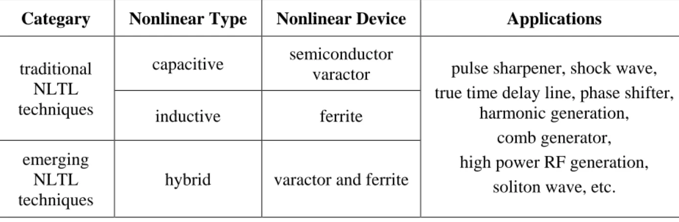
Table 1.1: Comparison of traditional and emerging passive nonlinear devices. ... 2
Table 1.2: Comparison of traditional and emerging nonlinear transmission line (NLTL) techniques. ... 25
Table 2.1: Description of circuits reported in Fig. 2.2 ... 34
Table 2.2: Value of equivalent model elements shown in Fig. 2.12. ... 59
Table 3.1: Comparison with the state-of-the-art work of electronic impedance tuner... 75
Table 4.1: Studies of power-handling capacity and nonlinearity of EIS. ... 93
Table 4.2: Final dimension of non-uniform distributed EIS. Unit: capacitor: pF; impedance: Ω; distance: mm. ... 103
LIST OF FIGURES
Figure 1.1: Energy band diagram of PN junction diode. ... 3
Figure 1.2: IV characteristic of conventional PN junction diode. ... 4
Figure 1.3: Junction capacitance-voltage characteristic of PN junction diode. ... 5
Figure 1.4: Point-Contact diode. (a) Construction and constituents and (b) p-region around point contact [1]. ... 6
Figure 1.5: Schottky diode. (a) Point-contact type, (b) deposited metal type [1]. ... 7
Figure 1.6: Energy band diagram for ideal Schottky barrier junction [2]. ... 7
Figure 1.7: Equivalent circuit of Schottky diode. ... 8
Figure 1.8: (a) Equivalent circuits of PIN diode; Simplified equivalent circuit (b) under forward bias and (c) under reverse bias [1, 2]. ... 10
Figure 1.9: Diagram of current and voltage waveforms of SRD [2]. ... 11
Figure 1.10: Equivalent circuit of SRD [2]. ... 12
Figure 1.11: Energy bands of tunnel diode at zero-bias condition [1]. ... 13
Figure 1.12: Current-voltage characteristic of tunnel diode. ... 13
Figure 1.13: Current-voltage characteristic of backward diode. ... 14
Figure 1.14: Operation mechanism of double-barrier RTD. Energy bands for three different bias (a)-(c); (d) IV curve of RTD. ... 15
Figure 1.15: Schematic diagram of IMPATT diode. ... 18
Figure 1.16: (a) Cross-sectional view and (b) equivalent circuit of resistive contact MEMS switch [2]. ... 20
Figure 1.17: (a) Cross-sectional view and (b) equivalent circuit of capacitive contact MEMS switch [2]. ... 21
Figure 1.18: Description of the device (sketch on the right not to scale). Elliptical pillars have a typical section of 85nm x 220nm [27]. ... 22
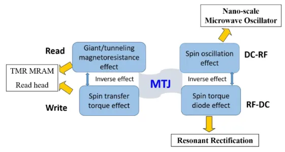
Figure 1.20: Spin torque diode effect. ... 24
Figure 1.21: Measurements and modeling results of differential resistance of devices obtained by taking the first derivative of voltage with respect to current. ... 24
Figure 1.22: IV characteristic of spindiode. Transitions between the two magnetic states of a spindiode are obtained for an applied voltage of 600 mV for AP and -600 mV for P-to-AP. ... 25
Figure 1.23: Circuit diagram of varactor-loaded NLTL. ... 26
Figure 1.24: Equivalent LC circuit of varactor-loaded NLTL. ... 26
Figure 1.25: (a) Cross sectional diagram and (b) 3D model of the ferrite-loaded NLTL [48]. ... 27
Figure 1.26: (a) Characteristics of nonlinear inductance and capacitance; (b) variation of delay and characteristic impedance with bias [72]. ... 29
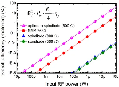
Figure 2.1: Maximum rectification efficiency that can be expected from state-of-the-art commercial rectifying devices. ... 32
Figure 2.2: State of the art microwave rectifier circuits (measurements). Color/shape of the scatters indicate on which nonlinear device a circuit of interest is based (see Table 2.1). Rectifiers that do not include matching circuit losses are not reported here. ... 33
Figure 2.3: Efficiency link of a rectifying circuit, from RF power to dc power. M stands for matching efficiency,
pis the efficiency associated with parasitic losses, 0is the efficiency of conversion that takes place in the nonlinear device (core conversion), and
DC transfer_ is the efficiency of dc power transfer from the nonlinear device to the dc load. (A full rectenna would also include the antenna radiation efficiency and dc/dc converter efficiency). The efficiency link is illustrated in Fig. 2.7 for SMS7630 diode. ... 35Figure 2.4: Model of a nonlinear component used in the analysis of this section. ... 37
Figure 2.5: I (V) curve of Skyworks SMS7630 low barrier Schottky diode (red dots) and M/A-COM MAE1317 high barrier Schottky diode ... 41 Figure 2.6: Differential resistance of the devices obtained by taking the first derivative of the voltage with respect to the current (Data calculated from the spice model). Under high
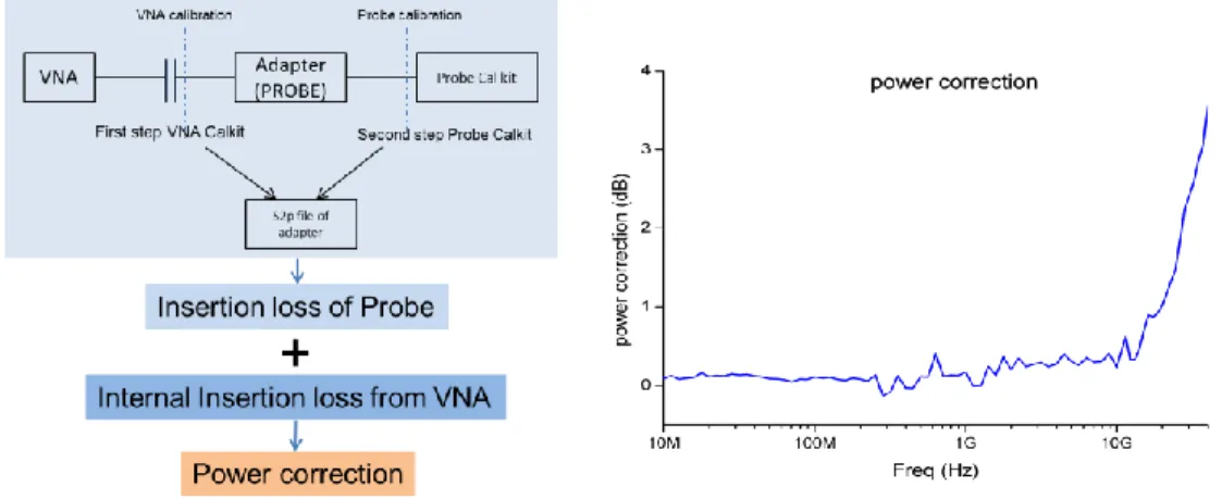
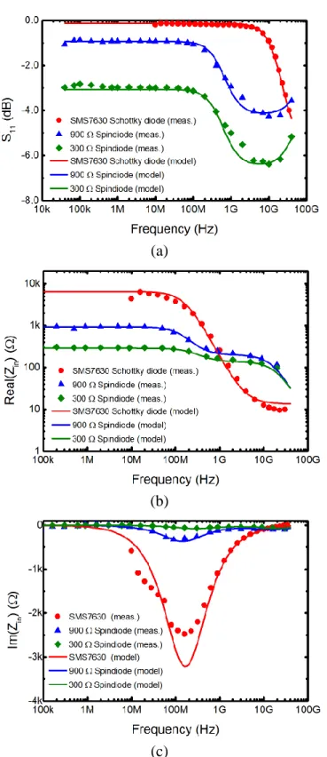
bias (> 100mA), the differential resistance is very close to the series resistance (𝑅𝑠). Also, under low bias (< pA), the value tends to the Zero Bias Resistance (ZBR). Note that in reality, differential resistance does not reach value higher than few hundreds of kilo-Ohm due to leakage current in the device. ... 42 Figure 2.7: Study of the losses in a rectifying circuit based on the SMS7630 diode. Result are given considering a perfect matching and no circuit losses based on circuit simulation (ADS). The low power analytical model described in section 2.1 is plotted with boxes. Frequency is 2.45GHz and output load is 1 kΩ. ... 42 Figure 2.8: Photograph describing the Schottky diode MACOM MA4E13 (left) and the on-wafer spindiode (right) from Everspin Technologies. Three pads are used for measurement purposes using a Ground-Signal-Ground (GSG) RF probe. The spindiode area is less than 0.015µm² and is therefore not visible on the microscope image. Its location is indicated by a black dot. ... 44 Figure 2.9: The frame and front panel of the developed program for spin diode measurement. ... 45 Figure 2.10: Schematic diagram of the setup based on Vector Network Analyzer that is used to measure voltage coefficient, the voltmeter is assigned to measure the non-resonant rectification through a bias-T. ... 45 Figure 2.11: Power calibration with de-embedding technique and power correction. ... 46 Figure 2.12: Equivalent MTJ model with nonlinear description of junction resistance and high frequency parasitic components. Test pads effect is not shown in this model. ... 47 Figure 2.13: Real and imaginary parts (Re(Z) and Im(Z), respectively) of the impedance for two MTJs with different junction areas (a) 0.02 and (b) 0.0096 μm2 in both AP and P states. The points with error bar denote the experimental data while the solid lines represent the simulation data using the model. ... 49 Figure 2.14: (a) - (d) Parametric study of interfacial resistance and interfacial capacitance with error bar in both AP and P state. (e) Calculated geometrical capacitance for all of the samples with different bit area. Circle and cross denote the samples with short axis 63 nm and 85 nm, respectively, while star and triangle denote the samples with short axis 100 nm and 120 nm, respectively. ... 50
Figure 2.15: (a) 3-D electromagnetic model of test pads, in which the wave port is defined as port 1, and the lumped port is defined as port 2. (b) Equivalent circuit model in ADS. (c) Comparison of S-parameters from two simulations. ... 51 Figure 2.16: (a) Matched sensitivity calculated from measurement of rectified voltage and injected power, considering the uncertainty from VNA and volt-meter. (b) Stacked area chart of power distribution analysis for the 0.02 μm2 MTJ sample, the gray part stands for the power reflected towards the generator, the orange part represents the power passing through the nonlinear junction resistance and the green part represents the power consumed in the series resistance Rs and interfacial resistance Ri. ... 53 Figure 2.17: Extracted parasitic factor is used to evaluate the performance of MTJs at microwave frequencies. The points denote the experimental data of the 0.02 μm2 MTJ sample while solid lines are from simulation using the equivalent model. ... 54 Figure 2.18: Analysis of (a) junction resistance (b) voltage sensitivity when frequency tends to zero hertz, and (c) 3 dB cutoff frequency for all of samples in both AP and P state. The points are from measurements, the blue dash line is just a guide for the eyes. ... 54 Figure 2.19: (a) Complete model for MTJ including test pads effect. (b) Simplified model in order to analyze cutoff frequency. ... 55 Figure 2.20: Comparison of (a) S11, (b) real part and (c) imaginary part of impedance between two spindiodes with different junction resistances and a commercial SMS7630 Schottky diode. During measurement, power entering the nonlinear device was kept below – 40 dBm. ... 57 Figure 2.21: Efficiency related to the parasitic losses. Data shown are calculated as the square of measured responsivity, normalized to low frequency value, with a compensation of insertion losses. ... 58 Figure 2.22: Calculated dc responsivity from I(V) measurements results. The point located at
zero-bias indicates a low frequency low power measurements to validate the responsivity extraction. ... 59 Figure 2.23: Complex model of MTJ [130]. ... 61
Figure 2.24: Low power diode efficiency under the matched conditions and the load condition j L
R R . Data were calculated based on the measurement of responsivity, ZBR and parasitic
efficiency at 30 GHz... 61
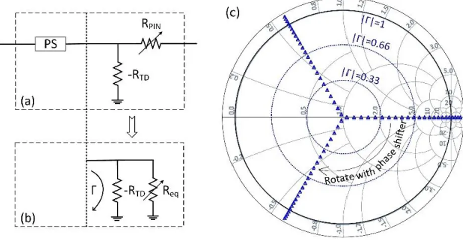
Figure 3.1: Diagram of electronic tuner: it consists of a wideband NLTL-based phase shifter and an impedance tuning circuit. ... 64
Figure 3.2: (a) Ideal circuit of the proposed topology; (b) Simplified circuit to generate impedance values; (c) Operation principle illustrated on Smith chart. ... 64
Figure 3.3: (a) Tunneling diode model with Symbolically Defined Devices (SDD), (b) I(V) curve and extracted resistance of tunneling diode MBD5057-E28X from MACOM Technology Solutions. ... 66
Figure 3.4: (a) SPICE model for PIN diode under forward bias; (b) Equivalent series resistance Rs of PIN diode SMP1320 from Skyworks Solutions Inc. ... 66
Figure 3.5: LC model of unit cell of NLTL. ... 67
Figure 3.6: LC model of unit cell of NLTL with loss. ... 69
Figure 3.7: Diagram of design procedure of NLTL-based phase shifter. ... 70
Figure 3.8: Design results of NLTL-based phase shifter. ... 71
Figure 3.9: Photo of the fabricated electronic impedance tuner. ... 72
Figure 3.10: Measured phase difference of the NLTL-based phase shifter. ... 73
Figure 3.11: Measured 25740 impedance states for the proposed electronic impedance tuner at (a) 1.5 GHz, (b) 2 GHz, (c) 2.5 GHz, (d) 3 GHz, (e) 4 GHZ, and (f) 5 GHz. The blue circle in (a) and (f) stands for the reflection coefficient equals to 1. ... 73
Figure 4.1: Topology of non-uniform EIS consists of an adjusting circuit and a distributed circuit. ... 79
Figure 4.2: Illustration of the effect of the adjusting circuit. Impedance distribution on Smith chart when PIN diode is (a) ON, and (b) OFF; (c) the total effect of the adjusting circuit on the improvement of Smith chart coverage. ... 79
Figure 4.3: (a) Predefined 1116 impedance points on Smith chart; (b) measured impedance points; (c) selected measured points; and (d) selected predefined points. ... 81 Figure 4.4: Impedance movement after (a) loading capacitance on the capacitive part of Smith chart, (b) loading with C N / 4 (N = 12), (c) loading with capacitance on the inductive part of Smith chart; (d) Required constant reflection coefficient circle. ... 83 Figure 4.5: Lower and upper boundaries of loading capacitance. ... 83 Figure 4.6: (a) Transmission response and (b) loss feature of EIS with fBragg of 3 GHz, 4 GHz and 5 GHz. Only the conductive loss and dielectric loss are taken into consideration in the total loss. The ripples in transmission response are because of the mismatching at this impedance state. Note that it is only the response of the impedance state with all the PIN diode turned ON. ... 84 Figure 4.7: The investigation of (a) Smith chart coverage as well as (b) mean loss of the EIS with different number of sections while keeping fBragg as 4 GHz. Mean loss is the average loss for the selected impedance points. Reactive parasitic parameters from commercial PIN diode and capacitor are not taken into consideration in the loss. ... 85 Figure 4.8: Nonlinearity of (a) Rs (IF) and (b) CT (Vr) characteristics of PIN diode SMP1320. IMD test for both (c) OFF and (d) ON states. Dots denote measurement while line denotes theoretical predictions. ... 87 Figure 4.9: Four different scenarios to use EIS: (a) Calibration with VNA; (b) Load-Pull characterization system; (c) Noise measurement; (d) TMN for reconfigurable PA or antenna. ... 89 Figure 4.10: The division of Smith chart to calculate the uniformity factor. ... 91 Figure 4.11: Traditional topology of distributed electronic impedance synthesizer. ... 92 Figure 4.12: Diagram for voltage distribution analysis. (a) Equivalent circuit of (m-1)th section; Thevenin equivalent circuit (b) at node m-1 with open termination; (c) at node m with open termination; (d) at node m with load. ... 95
Figure 4.13: Equivalent unit circuit model with PIN diode at (a) ON state, and (b) OFF state. Loading capacitor is still considered as ideal capacitor in order to keep the calculation concise. The biasing circuit is not shown in the model. ... 95 Figure 4.14: Diagram of optimization process using PSO. ... 97 Figure 4.15: Fabricated uniform and non-uniform circuits, biasing wires are not shown. (a) Circuit 1: 12 section uniform distributed topology without adjusting circuit. (b) Circuit 2: 12 section uniform distributed topology with one section of adjusting circuit. (c) Circuit 3: 12 section non-uniform distributed topology with one section of adjusting circuit. (d) Circuit 4: New 13 section non-uniform distributed EIS with one section of adjusting circuit. ... 100 Figure 4.16: (a) Comparison of measured and theoretically calculated Smith chart coverage for four fabricated circuits. ... 101 Figure 4.17: Equivalent circuit model of a unit circuit when PIN diode is turned (a) ON and (b) OFF. ... 101 Figure 4.18: Comparison of measured and theoretical S parameters for impedance states with all PIN diodes are turned (a) ON and (b) OFF. Dots denotes measurement, while solid line denotes theory. ... 104 Figure 4.19: (a) All 16384 measured impedance points; (b) Selected points for the calculation of Smith chart coverage. ... 105 Figure 4.20: (a) Measured and (b) theoretical impedance distribution at 1.2 GHz; (c) Measured and (d) theoretical impedance distribution at 1.5 GHz; (e) Measured and (f) theoretical impedance distribution at 1.8 GHz; (g) Measured and (h) theoretical impedance distribution at 2.1 GHz; (i) Measured and (j) theoretical impedance distribution at 2.4 GHz. The blue circle represents the constant VSWR=15 circle (|Γ|=0.875). ... 108 Figure 4.21: The comparison of measured and theoretically calculated uniformity factor. ... 109 Figure 4.22: Comparison of required Γ (black dash line), estimated maximum Γ (red solid line), theoretical maximum Γ (orange solid line with circle marker), and measured maximum Γ (blue solid line with triangle marker). ... 109
Figure 4.23: (a) Theoretical and (b) measured loss for the selected impedance points at 1.5 GHz; (c) Comparison of theoretical and measured mean loss over frequency. ... 110 Figure 4.24: Comparison of theoretical and simulated voltage distribution along the transmission line under average power of 0.5 watt for the (a) highest Г state (|Γ|=0.9) and (b) lowest Г state (|Γ|=0.01). ... 111 Figure 4.25: Simulated relationship of (a) P1 dB and (b) IIP3 with the maximum peak voltage along the transmission line for 20 impedance points under input power of 0.5 watt. Solid line is the linear fitting curve of the selected 20 points, while the dash line is the extension of the fitting curve. ... 112 Figure 4.26: Noise figure of the proposed non-uniform EIS at 1.5 GHz for 816 selected impedance states. ... 114 Figure 5.1: Equivalent circuit model of fully distributed hybrid NLTL per unit length. ... 116 Figure 5.2: Equivalent LC circuit model of unit cell of periodically loaded hybrid NLTL. ... 118 Figure 5.3: Permeability tensor elements and effective permeability versus magnetic bias. ... 121 Figure 5.4: Gyromagnetic resonance frequency versus external magnetic bias. ... 122 Figure 5.5: Effective permeability versus external magnetic bias at different operation frequency.
... 123 Figure 5.6: Effective permeability versus operation frequency at 0.44 tesla magnetic bias condition.
... 123 Figure 5.7: (a) Free space measurement [196], (b) air-filled coaxial line configuration [192], (c) waveguide configuration [185]. ... 124 Figure 5.8: (a) Measured S-parameters, (b) extracted impedance, (c) extracted permittivity and (d) extracted permeability. ... 125 Figure 5.9: Diagram of setup of air-filled coaxial line. ... 126 Figure 5.10: (a) windowed and (b) windowed real part of time domain impedance, (c)
Figure 5.11: Frequency domain response of impedance with and without time domain smoothing technique. The gray region indicates the truncated frequency range. ... 133 Figure 5.12: Extracted permittivity with and without time domain smoothing technique. The gray region indicates the truncated frequency range. ... 133 Figure 5.13: Extracted permeability with and without time domain smoothing technique. The gray region indicates the truncated frequency range. ... 134 Figure 5.14: Extracted effective permittivity at three frequencies for NLTL with varactor. ... 135 Figure 5.15: Extracted effective permittivity at three frequencies for YIG-based circuit. ... 136 Figure 5.16: Calculated characteristic impedance of hybrid NLTL when tuning the internal magnetic bias and reverse voltage bias. ... 137 Figure 5.17: Calculated phase velocity of hybrid NLTL when tuning the internal magnetic bias and reverse voltage bias. ... 138
LIST OF SYMBOLS AND ABBREVIATIONS
ADS Advanced Design SystemAP Anti-parallel
BST Barium strontium titanate C(V) Capacitance-voltage
CMOS Complementary Metal-Oxide-Semiconductor Transistor CPW Coplanar waveguide
CW Continuous wave dc Direct current DUT Device under test
EIS Electronic impedance synthesizer FCC Federal Communications Commission FMR Ferromagnetic resonance
FOM Figures of merit GaAs Gallium arsenide
GMR Giant magnetoresistance GSG Ground-Signal-Ground
GPIB General Purpose Interface Bus HB Harmonic Balance
HFSS High Frequency Structural Simulator IIP3 Input third-order intercept point IMD Intermodulation Distortion IMPATT IMPact Avalanche Transit Time IP3 Third-order intercept point I(V) Current-voltage
LC Inductance-capacitance
MEMS Microelectromechanical Systems MIM Metal-Insulator-Metal
MMIC Monolithic microwave integrated circuit MPH Microwave power harvesting
MPT Microwave power transfer MR Magnetoresistance
MRAM Magnetic random access memory MTJ Magnetic tunnel junction
NLTL Nonlinear transmission line
NVNA Nonlinear Vector Network Analyser
P Parallel
PA Power amplifier PCB Printed circuit board PIN P-Intrinsic-N
PSO Particle Swarm Optimization RF Radio frequency
RTD Resonant tunneling diode SDD Symbolically Defined Devices SRD Step recovery diode
ST-FMR Spin-torque-driven ferromagnetic resonance TED Transferred electron device
TMN Tunable matching networks TMR Tunnel magnetoresistance VNA Vector Network Analyser VSWR Voltage standing wave ratio WPT Wireless power transfer YIG Yttrium Iron Garnet ZBR Zero-bias resistance
CHAPTER 1
INTRODUCTION
Modern wireless and communication systems are heavily dependent on nonlinear circuits such as power amplifier (PA), mixer, multiplier, oscillator, switch, etc., the core of which are passive nonlinear devices (e.g. diodes) or active nonlinear devices (e.g. transistors). The term “nonlinear” intuitively means that the output signals and input signals are not in a linear relationship, it essentially indicates that one parameter is nonlinear with voltage or current. It should be noted that it is different from the nonlinearity of frequency responses, for instance, dispersion.
In this work, we focus on passive nonlinear devices. One purpose of this thesis is to provide a way for the readers to understand and choose proper nonlinear devices in accordance with different applications. Traditional nonlinear devices in terms of the categories of resistive, capacitive and inductive are firstly investigated in the following.
As listed in Table 1.1, the resistive devices include conventional PN junction diode, Point-Contact diode, Schottky diode, PIN diode, Step-Recovery diode (SRD), Metal-Insulator-Metal (MIM) diode, Tunnel diode (Esaki diode), Backward diode, Resonant Tunneling diode (RTD), Gunn diode, IMPATT diode, etc. [1, 2], among which the last five diodes present a differential negative resistance region in their current-voltage (I(V)) characteristics. The basic physical construction, operation principles as well as characteristics and applications for various types of diode are explained and compared.
The capacitive nonlinear devices include semiconductor and ferroelectric ceramics, whereas the inductive nonlinear devices usually use ferrite and other magnetic materials. Emerging nonlinear devices includes microelectromechanical system (MEMS) devices and spindiodes.
Nonlinear transmission line (NLTL) is a transmission line periodically loaded with nonlinear devices. Traditional NLTL technique uses either capacitive nonlinear devices (varactor, BST, PZT etc.) or inductive nonlinear devices (saturated ferrite). Emerging hybrid NLTL technique uses both nonlinear capacitive and inductive devices.
Table 1.1: Comparison of traditional and emerging passive nonlinear devices.
Categary Nonlinear Type Nonlinear Device Specialty Applications
traditional nonlinear
devices
resistive
PN junction diode detector, rectifier, modulator, switch, demoudulator circuit, etc.
point-contact diode mixer, detector, etc
Schottky diode detector, mixer, rectifier, etc.
PIN diode switch, attenuator, phase shifter, limiter, modulator, etc.
step-recovery diode short pulse generator, frequency multiplier, comb generator, etc.
MIM diode Mixer, rectifier, etc.
tunnel diode
negative resistance
oscillator, amplifier, mixer, detector, etc.
backward diode detector, rectfier, switch, etc.
RTD Oscillator, switch, etc.
Gunn diode Oscillator, amplifier, radar speed gun,
etc.
IMPATT diode power generation, etc.
capacitive
semiconductor varactor
VCO, parametric amplifier, harmonic generator, frequency multipliers, mixer,
microwave signal synthesizers, tunable circuit, etc.
BST
phase shifter, capacitor, DRAM, etc. PZT
inductive ferrite
tunable filter, oscillator, amplifier, circuilator, isolators, phase shifter, bandstop filter, magnet recording, etc. emerging
nonlinear devices
MEMS devices phase shifters, tunable filters, impedance tuners, oscillators, mixer, switch, etc.
MTJ MRAM, oscillator, rectifier, etc.
1.1 Traditional RF and microwave nonlinear devices
1.1.1 Resistive nonlinear devices
1.1.1.1 Conventional PN junction diode Construction
The conventional PN junction diode is the most basic and simplest solid state electronic device. It is constructed by the combination of P-type and N-type of semiconductors [1, 2]. By doping an
intrinsic semiconductor with acceptor impurities, a P-type semiconductor is formed, in which holes are the majority carriers while electrons are the minority carriers. The term P-type denotes the positive charge of the hole. As opposed to P-type semiconductors, N-type semiconductors are formed by doping an intrinsic semiconductor with donor impurities, in which free electrons have a more massive concentration than holes. The term N-type refers to the negative charge of the electron.
Figure 1.1: Energy band diagram of PN junction diode. Operation principle and characteristics
As depicted in Fig. 1.1, a PN junction will be formed when a P-type semiconductor is placed in contact with a N-type semiconductor. The density gradient at both sides of the PN junction results in the free holes in P-type side that diffuse across the interface and recombine when they reach N-type side, and leave behind the fixed negatively charged acceptor ions. Similarly, it also results in the free electrons that diffuse from N-type side to P-type side, and leave behind the fixed positively charged donor ions. The negatively and positively charged ions will create an electrostatic potential barrier, which will prevent the diffusion of free charge carriers. A depletion layer will be formed when an equilibrium state will be reached, and no free charge carriers will exist in this layer. The extra energy that is required to overcome the barrier is called the barrier potential, which depends on the semiconductor material, doping level as well as temperature, and is about 0.7 V for silicon and 0.3 V for germanium.
Opposite to the diffusion current that is caused by the majority carriers, the drift current is due to the minority carriers that are moving across the junction and accelerated by the barrier potential. In
the unbiased condition, the net current is zero since the drift current and diffusion current are equal to each other.
Ohmic effects
In the forward bias condition, the P-type and N-type semiconductors are connected with the positive and negative electrode of the voltage source, respectively. The external voltage can push the majority carriers (holes) in the P-type side and the majority carriers (electrons) in the N-type side toward and then neutralize the depletion layer so that the width of the depletion layer is reduced. There is almost no current when the external voltage is less than the barrier potential since the free electrons and holes cannot overcome the barrier. As shown in the I(V) characteristic of PN junction diode in Fig. 1.2, with the increases of the forward bias, the depletion zone decreases, eventually results in an electrical resistance reduction. The relationship of IV characteristic of PN junction diode can be expressed as [2]
( ) ( 1) s q V IR nKT s I I e (1.1)
where Is is the reverse saturation current, q is the electron charge, V is the external bias, Rs is the series resistance of PN junction, n is ideality factor, K is Boltzmann constant, and T is absolute temperature.
In the reverse bias condition, the P-type and N-type semiconductors are connected with the negative and positive electrode of the voltage source, respectively. The reverse bias pulls the holes in the P-type side and electrons in the N-P-type side away from the junction, which increases the width of the depletion layer, so that results in a high resistance allowing a small current across the junction. As shown in Fig. 1.2, when the reverse bias increases beyond a critical level, the depletion region breaks down and current begins to flow, and it is called the avalanche effect.
Junction capacitance
Two types of capacitance mechanisms are involved in PN junction, namely depletion capacitance and diffusion capacitance, respectively, as shown in the capacitance-voltage (C(V)) characteristic of a PN junction diode in Fig. 1.3. The depletion capacitance is caused by the impurity atoms, and it dominates under the reverse bias condition. It can be calculated as [2]
0 0 (1 ) j C C V V (1.2)
where C0 is the zero-bias capacitance, V is the reverse bias voltage, V0 is built-in potential, γ is a constant, it is 1/2 for an abrupt junction, 1/3 for a graded junction, and 1 to 2 for a hyperabrupt junction. The diffusion capacitance is caused by the injected minority charge, and it dominates under the forward bias condition. It is proportional to the minority carrier lifetime, therefore related to the switching characteristic of the PN junction diode.
Application
The PN junction diodes can be found in the applications of detector, rectifier, modulator, switch, demodulation circuit, clamping circuit, clipping circuit, clamping circuit, etc. [2]
1.1.1.2 Point-Contact diode Construction
Similar to conventional PN junction, Point-Contact diode is also one of the most basic forms of diodes. It has been developed during the Second World War, and is often used as mixer or detector. As depicted in Fig. 1.4, it is made by a cat whisker metal wire placed on a piece of N-type semiconductor [1, 2]. During the formation of a Point-Contact diode, a relatively high current will pass through the cat whisker wire to the semiconductor, part of the metal will migrate into the semiconductor, a small P-type region will be formed in the vicinity of the point contact, thus a PN junction is formed which behaves the same as a conventional PN junction.
Figure 1.4: Point-Contact diode. (a) Construction and constituents and (b) p-region around point contact [1].
Operation principle
The operation mechanism of Point-Contact diode is quite similar to a conventional PN junction diode. However, the characteristics are different under forward and reverse bias conditions, mainly because of the small contact between the cat whisker and the semiconductor. The resistance of Point-Contact diode in the forward bias condition is larger than the conventional PN junction diode, while the capacitance in the reverse bias condition is smaller. The very low junction capacitance
leads to a better switching ability than a conventional PN diode, thus ideal for many RF applications. However, the small junction also limits the power handling of a high current [1].
Applications
With the advantages of fast switching and the small junction capacitance due to small junction area, Point-Contact diode is suitable for high-frequency applications, such as mixer, detector, etc. [1]. 1.1.1.3 Schottky diode
Construction
The Schottky diode can be considered as a variation of point-contact diode, it can be manufactured in different forms, in which the simplest form is a point-contact diode (Fig. 1.5(a)). As shown in Fig. 1.5(b), the metal-semiconductor junction in the deposited metal Schottky diode is a surface rather than a point contact [1]. A large contact area between the metal and the semiconductor enables a low forward resistance and low capacitance.
Figure 1.5: Schottky diode. (a) Point-contact type, (b) deposited metal type [1]. Operation principle and chracteristics
In a metal, the energy gap between the valence band and conduction band is too small, so that it is conductive. By contrast, no free electron exists at the Fermi level in the semiconductor because the Fermi level lies within the energy gap. When a metal contacts with a semiconductor, a Schottky junction is formed, and the Fermi levels must align, the energy band diagrams for the Schottky junction is illustrated in Fig. 1.6 [2]. Since the work function of the metal is greater than that of the semiconductor, an electrostatic barrier is formed, which enables a Schottky diode to have the rectifying properties.
The current-voltage characteristics of a Schottky diode is similar to that of a PN junction diode. However, there are still some differences: by using the same semiconductor material, the reverse leakage current of a Schottky diode is higher, and the reverse breakdown voltage is lower than a PN junction diode. While at a specific forward current, the forward voltage for a Schottky diode is lower than a PN junction diode.
Equivalent circuit model
The equivalent circuit model of PN junction diode is shown in Fig. 1.7 [2, 3]. Cj and Rj represent the nonlinear junction capacitance and junction resistance, respectively. Rs denotes the total series resistance that includes the resistance of the epitaxial layer and the substrate, Ls denotes the series inductance, and Cp represents the packaging capacitance.
Figure 1.7: Equivalent circuit of Schottky diode. Applications
Similar to the point-contact diode, the Schottky diodes can be used in applications requiring high switching speed, high power and high frequency capacity. They have the following advantages [1]: (i) Low turn-on voltage due to the high current density, it is 0.2 - 0.3 V for a Silicon Schottky diode that is similar to a germanium PN junction diode. The less waste of energy makes them suitable for the applications that require high efficiency; (ii) High frequency capacity and fast recovery time
due to almost no minority carrier charge storage. Unlike the conventional PN junction diode that relies on the recombination of holes or electrons when they move to the other side of semiconductor, Schottky diode is a majority carrier device; (iii) Low noise generation; (iv) Low forward resistance; (v) Low junction capacitance due to the small contact area. The reduction of RC time constant makes them faster than the conventional PN junction diodes, which enables them suitable for many applications requires fast speed. The characteristics of low parasitic parameters and fast recovery time make them suitable for high frequency applications.
1.1.1.4 PIN diode Construction
PIN stands for P-Intrinsic-N, it is a PN junction device. Located between the P-type and N-type semiconductors, a minimally doped thicker layer or an intrinsic semiconductor is inserted, so that a high resistivity is presented. PIN diodes are usually constructed on Silicon due to its better power-handling capability, however, GaAs can be chosen if higher speed is required [1].
Operation principle and characteristics
When a PIN diode is forward biased, holes and electrons are injected from P-type and N-type region into the intrinsic region (I-region), respectively. Instead of combining immediately, a finite quantity of charges will remain in the I-region. The quantity of charges relies on the recombination time or carrier-lifetime as well as the forward bias current. The thick intrinsic layer increases the transit time for electrons to cross the I-region, resulting in the accumulation of electrons in the I-region. PIN diode acts as a traditional rectifying device up to about 100 MHz, and beyond this frequency, the storage of charges in the I-region makes the diode act as a variable resistance[1].
When PIN diode is reverse biased, the reverse current flows until the I-region is depleted of charges. The switching time or recovery time is defined as the time required to remove the charges stored in the I-region due to the forward bias. When PIN diode is used as switch, the switching time can be understood as the time to switch from a low-impedance state (forward bias) to a high-impedance state (reverse bias) [1].
Figure 1.8: (a) Equivalent circuits of PIN diode; Simplified equivalent circuit (b) under forward bias and (c) under reverse bias [1, 2].
Equivalent circuit model
The equivalent circuit of PIN diode is described in Fig. 1.8(a) [2], it mainly consists of two sets of elements in series: the first part is similar to a PN junction, it includes diffusion capacitance Cd in parallel with junction resistance Rj and junction capacitance Cj; while the second part consists of the undepleted I-region resistance Ri and capacitance Ci. Besides the core parts, Ls denotes the lead inductance, Rs represents the resistance of the bulk semiconductor and the contacts, Cp denotes the packaging capacitance, Cf represents fringing capacitance of the structure which can be neglected as compared to other capacitances.
Although the model shown in Fig. 1.8(a) can describe the physical model, it is not practical in the circuit design. It can be simplified for both forward bias and reverse bias conditions. Under the forward bias condition, the diffusion capacitance Cd is large so that shorts out the junction parameters. The charge carriers will be injected into the I-region, the Ci will vanish so that only Ri left. The equivalent circuit for the forward bias condition is simplified as Fig. 1.8(b) [1, 2, 4, 5], Rt is the total RF resistance (Rs plus Ri), which is a current-controlled resistance.
Under the reverse bias condition, the diffusion capacitance Cd vanishes, and the junction resistance Rj becomes large, only Cj remains. The Ri-Ci part will vanish if the reverse bias is high enough to deplete the I-region. The equivalent circuit for a reverse bias condition will be simplified as Fig. 1.8(c) [1, 2, 4, 5].
Applications
The presence of the intrinsic layer provides two benefits for the reverse bias condition: high breakdown voltage so as to have high power handling capacity, small junction capacitance due to
the separation between P-type and N-type semiconductors. The benefits make PIN diode useful for high frequency and high power rectification application. Under the forward bias condition, the I-region is controlled by the amount of injected charge carriers, which makes the possibility to control the large RF signal with a small level of dc excitation. It is extensively used in the low loss and low distortion applications, for instance, RF switches, attenuators, phase shifters, limiters and amplitude modulator, etc. [1, 2].
1.1.1.5 Step-Recovery diode (SRD) Construction
A SRD is usually constructed upon the PIN structure, although in principle it can be constructed on any diode structure. The difference with PIN diode is that the SRD is fabricated with gradually decreased doping level as the close of the junction, which results in fewer charge carriers stored in the I-region so as to have shorter switching time [1, 2]. This advantage makes SRD suitable for applications that require fast switching.
Operation principle and characteristics
The operation of a SRD relies on the charges storage and extraction characteristics in the semiconductor. As illustrated in Fig. 1.9, in the positive conduction region (forward bias), the SRD operates like a normal diode, the RF current will follow the RF voltage waveform, the charges will be stored in the I-region of the diode. In the negative portion of the RF voltage cycle (reverse bias), the charges start to extract from the I-region. Once the free charges are removed from the I-region, the RF current suddenly reduces to zero in a very short time. The rapid vanish of current in time domain stands for rich harmonics in frequency domain.
Figure 1.10: Equivalent circuit of SRD [2]. Equivalent circuit model
The equivalent circuit of the SRD can be modeled by combining the forward- and reverse-biased circuit with a switch, as shown in Fig. 1.10, in which the series resistance Rs denotes the voltage drop across the diode [2]. The switch is closed under the forward bias condition, the circuit consists of a relatively large diffusion capacitance Cf, accounting for the large charge storage in the I-region, in shunt with a resistance Rf. Under the reverse bias condition, the switch is still closed until all the charges are extracted from the diffusion capacitance Cf, the circuit also includes the depletion layer capacitance Cr.
Applications
Due to the fast switching times characteristic, the SRD is suitable for the applications of short pulse generator, high-efficiency high-order frequency multiplier, comb generator, etc. [1, 2].
1.1.1.6 Tunnel diode (Esaki diode) Construction
Tunnel diode, also called Esaki diode, has a junction that enables tunneling transport, classically use P-type and N-type semiconductors. The semiconductors are heavily doped with impurity, resulting in a depletion layer thin enough for majority carriers to cross by tunneling [1]. Since it is the movement of majority carriers, the operation of tunnel diode is faster than conventional PN junction diode. Different from the conventional transit time concept, the time of tunneling is proportional to quantum transition probability.
Figure 1.11: Energy bands of tunnel diode at zero-bias condition [1]. Operation principle and characteristics
Fig. 1.11 illustrates the energy bands of tunnel diode at the zero-bias condition [1]. Only when the filled state at N-side and empty state at P-side are aligned at the same level, tunneling will occur. The current-voltage characteristic of a tunnel diode is presented in Fig. 1.12. When the applied forward bias increases, electrons start to tunneling from N-side to P-side, because the filled state at N-side starts to align at the same level with an empty state at P-side. When they are aligned exactly, the maximum current will be reached, after that the current starts to decrease until a very low level. With the further increases of bias, ordinary injection current starts to increase exponentially, which is similar to a PN junction diode.
Applications
Tunnel diode has advantages of high speed, low operation voltage, low noise generation, high peak current-to-valley current ratio, low cost and lightweight. It exhibits a negative resistance under the forward bias condition, thus can be used in microwave oscillators and amplifiers. It also can be used in microwave mixers, detectors, and binary memory.
1.1.1.7 Backward diode
The backward diode, is also a form of PN junction diode. The operation mechanism is similar to the tunnel diode, the difference is that backward diode operates by tunneling only under the reverse current condition. In the backward diode, doping level in one side of the junction is less than the other, the doping profile gives a freedom to modify some characteristics from the tunnel diode [6]. Operation principle and characteristics
Under the reverse bias, the tunneling effect of the backward diode is similar to the tunnel diode, while under the forward bias the tunneling effect reduces and it is similar to a conventional PN junction diode [6]. In other words, its name comes from the fact that the diode can be used backward.
As can be seen from Fig. 1.13, the forward IV curve is similar to a conventional PN junction diode. Zener breakdown starts at a low reverse bias voltage, the voltage remains relatively constant and is independent of the reverse current. It should be noted that the negative resistance region is not presented in the IV curve, because the tunneling phenomenon is only incipient.
Applications
The backward diode has a strong nonlinearity at a small signal region, and it does not have a charge storage effect so that it can be used as a detector and rectifier at high frequency (more than 40 GHz) with weak signals, and it also can be used for high speed switching applications [6].
1.1.1.8 Resonant tunneling diode (RTD)
Resonant Tunneling Diode (RTD) is a two-terminal quantum device, it consists of a quantum well locating between two quantum barriers. It works by the resonant tunneling effect so that negative differential resistance regions are often present in the current-voltage characteristics, which enables many high-speed applications. An RTD can be fabricated with a variety of semiconductor materials and different resonant tunneling structures [7, 8].
Operation principle and characteristics
Fig. 1.14 illustrates the operation mechanism of a double-barrier RTD [7, 8]. The charge carriers in the quantum well only can present at discrete energy states. As the bias of RTD increases, the first confined state is close to Fermi level, the current increases, as shown from point A to B in Fig. 1.14(d). As the bias further increases, the first confined state becomes lower than Fermi level and fall into the bandgap, the current decreases, as shown from point B to C in Fig. 1.14(d). When the second confined state is close to Fermi level, the current will increase again, as shown from point C to D in Fig. 1.14(d).
Figure 1.14: Operation mechanism of double-barrier RTD. Energy bands for three different bias (a)-(c); (d) IV curve of RTD.
Applications
Since the quantum tunneling effect through the thin barriers and quantum well is very fast, RTD is capable of enabling high-speed and high-frequency applications, such as oscillators and switching devices at terahertz frequencies [7, 8].
1.1.1.9 MIM Diode Construction
Metal-Insulator-Metal (MIM) diode is similar to a semiconductor diode, it consists of an insulating layer sandwiched two layers of metal [9-11]. It is based on the tunneling mechanism. The insulating layer should be thin enough in the order of tens of atom layers for the tunneling. The fabrication process of thin film deposition for an insulating layer with a few nanometers thickness was achieved in the 1960s, the simple materials and fabrication technology make the MIM diode more competitive with other techniques. Multiple insulating barriers can be built in MIM diode to overcome the thermal voltage limitation of a Schottky diode [9, 12].
Operation principle and characteristics
Two operation mechanisms involve in a MIM diode, namely quantum tunneling and thermal activation (also called Schottky effect) [9, 13]. The geometry of the insulating layer, such as thickness, barrier height as well as temperature, will determine the domination of each mechanism. Tunneling will dominate only when the barrier is high and thin enough. The two mechanism can be sorted out by the measurements for MIM diodes with two barrier thicknesses at two different temperatures [14].
Applications
MIM diode can be used in the high-speed applications due to the tunneling mechanism and very low junction capacitance, for instance, a mixer at 148 THz [15]. It also could be used in the rectifier, the state-of-the-art MIM diode with multiple insulating layers has already presented very similar zero-bias current responsivity with the Schottky diode [9].
1.1.1.10 Gunn diode Construction
A Gunn diode is a type of transferred electron device (TED), it operates on the principle of Gunn effect that is discovered by physicist J.B. Gunn in 1963 [16]. It presents a negative resistance region. Unlike other semiconductor diode consisting of P- and N-type semiconductor materials, Gunn diode is composed of only N-type semiconductor material, therefore, it is not a unidirectional device. A Gunn diode consists of two heavily doped materials on the terminals, and a thin layer of lightly doped material in the middle [1].
Operation principle and characteristics
In Gunn diode, the conduction electrons transfer between different energy levels with the influence of the electric field, it is also referred to as TED. When the bias at the two terminals of the Gunn diode increases, the current increases. At a certain bias level, the resistivity of the thin middle layer increases, which results in the drop of the current. In other words, the Gunn diode presents a negative differential resistance region, in which the increases of the bias will cause a decrease in current [1].
Applications
The property of negative resistance allows the Gunn diode can be used in the amplification application at microwave frequency, such as amplifier, oscillator, etc. Gunn diode oscillator can be used in airborne collision avoidance radar, anti-lock brakes, radar speed guns, motion detector, air traffic control, millimeter-wave radio astronomy receivers [16].
1.1.1.11 IMPATT diode Construction
IMPATT (IMPact Avalanche Transit Time) diodes are semiconductor devices that use the properties of avalanche effect and transit time of semiconductors, also referred to as avalanche transit time devices. As illustrated in Fig. 1.15, IMPATT diode is made from a heavily doped N-type semiconductor layer (N+ layer), beside which another lightly doped layer (N layer) is deposited epitaxially. At the other terminal, P-type semiconductor layer is heavily doped (P+ layer) [1]. IMPATT diodes can be fabricated with Si, GaAs or InP. The Si-based IMPATT diode can work up
to above 200 GHz with high output and is cheaper due to the simple fabrication process. By contrast, the GaAs-based IMPATT diode has higher efficiency and lower noise than others.
Figure 1.15: Schematic diagram of IMPATT diode. Operation principle and characteristics
Although the structure of IMPATT diodes are similar to traditional Schottky or PIN diodes, the operation principle is quite different. Similar to a Schottky diode, it will break down at a certain level of reverse bias, the IMPATT diodes operate in this breakdown region and based on avalanche effect. When a certain level of reverse bias is applied, a high potential gradient is generated across the PN junction due to the narrow gap, which results in the acceleration of minority carriers. The accelerated carriers will collide with the crystal lattice, as a result more carriers will be freed and accelerated. This process will cause avalanche breakdown due to the fast multiplication of carriers [1, 17].
Applications
With the advantage of high-power capability, IMPATT diodes are used for solid-state microwave and millimeter wave power generation. Compared to Gunn diodes, IMPATT diodes are more efficient and have higher output power with lower power supply [1].
1.1.2 Capacitive nonlinear devices
1.1.2.1 VaractorA varactor is a type of PN junction, having the junction capacitance optimized for a reverse bias scenario. It presents a variable capacitance with the control of the reverse bias [1, 2].
![Figure 1.11: Energy bands of tunnel diode at zero-bias condition [1]. Operation principle and characteristics](https://thumb-eu.123doks.com/thumbv2/123doknet/2352824.36647/39.918.194.730.102.430/figure-energy-bands-tunnel-condition-operation-principle-characteristics.webp)