1 SUPPORTING INFORMATION
Structure Controlled Long-Range Sequential Tunneling in
Carbon-Based Molecular Junctions
Amin Morteza Najarian
1,2, Richard L. McCreery
1,2†1 Department of Chemistry University of Alberta
Canada,T6G 2R3
2 National Institute for Nanotechnology National Research Council Canada
Canada, T6G 2G2 † Corresponding author Tel.: 780-641-1760 Email: [email protected]
Content:
1. Junction fabrication2. Electrical measurements and JV curves
3. Linearity of ln J for Fluorene devices with various abscissas 4. UV-Vis absorption spectra of molecules
5. JV and lnJ vs V1/2 curves for NAB, AQ and BTB
6. Temperature dependence of JV responses 7. Schottky and Poole-Frankel mechanisms
2 1. Junction fabrication
Cross-bar molecular junction fabrication has three main steps: bottom contact fabrication, molecular layer grafting, and top contact deposition:
1.1 Bottom contact
Pyrolized photoresist film (PPF) electrode fabrication is described in detail elsewhere.1 Briefly, positive photoresist (AZ 4330) was spin coated on each sample, followed by a soft bake at 80 °C and then photolithography was carried out with a UV exposure. Development was done in a 1:3 dilution of AZ developer: water. Resulting four lines with 500 μm width were pyrolyzed in a 1-inch tube furnace by heating under a flow of forming gas (5% H2, balance N2) to 1050 °C for 1 hour. After cooling in flowing forming gas, the PPF surface consists of sp2 carbon similar to glassy carbon with RMS roughness lower than 0.5 nm.
1.2 Molecular layer grafting
Electrochemical reduction of diazonium species on the surface is used for grafting molecular layer on the surface of bottom contact (PPF). A conventional three-electrode electrochemical cell with Ag/Ag+ electrode as reference and Pt wire as a counter electrode was used for grafting. The solution was 1 mM diazonium salt of the molecule (AQ, NAB, FL) dissolved in acetonitrile containing 0.1 M tetrabutylammonium hexafluorophosphate (TBAPF6) as supporting electrolyte. The thickness of grafted molecular layer was controlled by sweeping the potential from 0.4 to −1.3 V (vs. Ag/Ag+) at 50 mV/s for repeated cycles. After modification, the sample was rinsed with acetonitrile and dried using a stream of nitrogen.
3
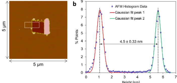
Measurement of molecular layer thickness was done using AFM “scratching” technique, using the same procedure described previously.2, 3 The example of the AFM measurement is shown in Figure S1. Thickness measurements were done adjacent to one of the junctions of each sample. First, contact mode was applied to scratch a trench (1 x 1 µm) in the molecular layer, then a 5 x 5 µm tapping mode image was then obtained in the area surrounding and including the trench (Figure S1-a). A histogram generated from the height data was fitted by two separate Gaussian functions (for the two different height distributions), with the height determined as the difference between the centers of the two functions and the uncertainty given as the quadrature addition of the two best-fit
σ values. Thicknesses mentioned in Table S1 are determined in the same way.
Figure S1. (a) AFM Tapping mode 5 x 5 µm tapping mode image of a 1 x 1 μm “trench” made in
a PPF/FL layer using contact mode AFM. (b) Histogram of heights determined within the white rectangle of the AFM image. Uncertainty in thickness is the quadrature addition of the two Gaussian σ values.
Electrochemical parameters used for deposition of molecular layers of AQ, FL and NAB are listed in Table S1. Parameters for BTB grafting are reported previously. 4
5 μm
5
μ
m
4
Table S1. Electrochemical parameters for grafting of molecule on the surface of PPF
Molecule Sweep range (V vs. Ag/Ag+) No. of cycles Scan rate (mV/s) Thickness (nm) Fluorene 0.4 – (-0.35) 6 50 2.3 ± 0.3 0.4 – (-0.40) 6 50 2.9 ± 0.3 0.4 – (-0.45) 7 50 3.4 ± 0.2 0.4 – (-0.50) 7 50 3.9 ± 0.4 0.4 – (-0.60) 8 50 4.1 ± 0.3 0.4 – (-0.70) 8 50 4.5 ± 0.3 0.4 – (-0.75) 8 50 5.0 ± 0.4 0.4 – (-0.80) 8 50 5.5 ± 0.4 0.4 – (-0.90) 8 50 6.1 ± 0.4 0.4 – (-1.0) 8 50 7.1 ± 0.5 0.4 – (-1.10) 10 50 7.6 ± 0.5 0.4 – (-1.20) 10 50 8.0 ± 0.7 0.4 – (-1.30) 10 50 8.6 ± 0.6 Anthraquinone 0.4 – (-0.20) 6 50 2.2 ± 0.3 0.4 – (-0.25) 6 50 2.9 ± 0.3 0.4 – (-0.30) 6 50 3.4 ± 0.4 0.4 – (-0.35) 8 50 3.9 ± 0.4 0.4 – (-0.40) 8 50 4.3 ± 0.4 0.4 – (-0.50) 8 50 5.5 ± 0.5 0.4 – (-0.55) 8 50 6.2 ± 0.5 0.4 – (-0.60) 8 50 7.1 ± 0.6 0.4 – (-0.65) 8 50 8.0 ± 0.5 0.4 – (-0.70) 8 50 8.9 ± 0.6 0.4 – (-0.75) 8 50 9.5 ± 0.6 0.4 – (-0.80) 8 50 10.6 ± 0.5 NAB 0.4 – (-0.30) 6 40 3.2 ± 0.3 0.4 – (-0.35) 6 40 4.1 ± 0.3 0.4 – (-0.4) 6 40 4.5 ± 0.4 0.4 – (-0.45) 8 40 5.1 ± 0.4 0.4 – (-0.5) 8 40 5.9 ± 0.5 0.4 – (-0.65) 8 40 7.4 ± 0.6 0.4 – (-0.80) 10 40 10.1 ± 0.6 0.4 – (-0.90) 10 40 11.9 ± 0.7
5
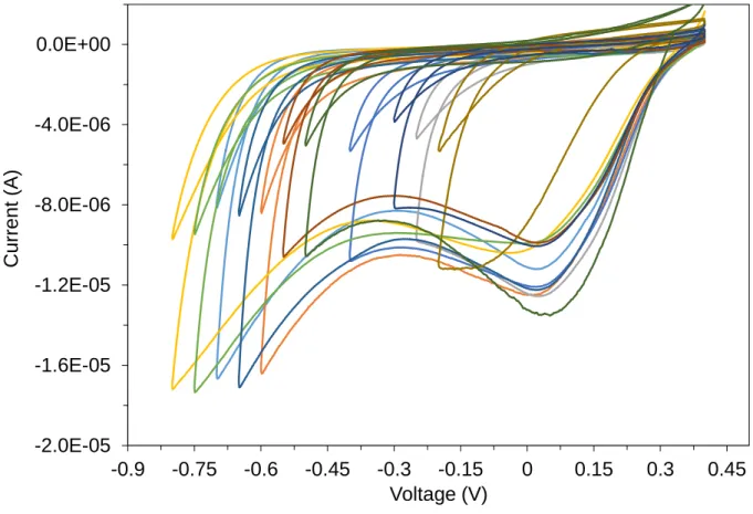
First two cycle of corresponding cyclic voltammograms for grafting of Anthraquinone molecular layer with parameters listed in Table S1 are shown in Figure S2.
Figure S2. Cyclic voltammograms during grafting of Anthraquinone on the surface or PPF, with
a variation of negative potential limit causing AQ layers with different thicknesses. -2.0E-05 -1.6E-05 -1.2E-05 -8.0E-06 -4.0E-06 0.0E+00 -0.9 -0.75 -0.6 -0.45 -0.3 -0.15 0 0.15 0.3 0.45 Curr e n t (A) Voltage (V)
6 1.3 Top contact deposition
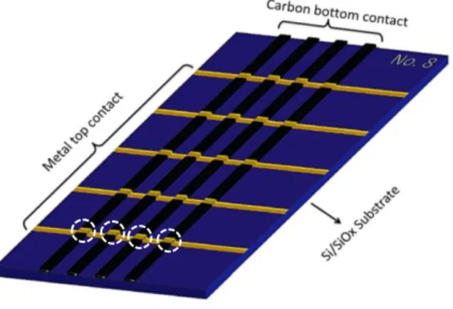
The top contact electrode was comprised of electron beam deposition of 10 nm eC and 15 nm Au through a physical shadow mask with 0.25 mm openings oriented perpendicular to the bottom contact, which results in a crossbar junction of 0.125 mm2 area. Deposition was done in an electron beam evaporator (Kurt J. Lesker PVD75) with typical pressure below 7 × 10⁻⁶ Torr in starting point of deposition. Deposition rate was 0.01 nm/sec for
eC and 0.03 nm/sec for Au. Characteristics of eC are investigated previously.5 The schematics of the final fabricated chip is shown in Figure S3. As indicated in the Figure with white circles, bottom four or six junctions are measured for all cases.
Figure S3. Schematics of fabricated chips. White circles identify PPF/molecule/eC/Au molecular
junctions
2. Electrical measurements and JV curves
All current–voltage curves were obtained using a Keithley 2602A source-meter in 4-wire mode. Measurements are all done in the air except temperature dependence measurement that they are done in a vacuum chamber with pressure below 10-5 Torr. The home-made program is used to acquire the data in order to have dynamic NPLC
7
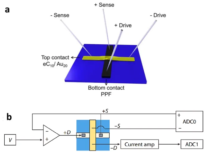
from 25 to 0.001 during the measurement based on the sensitivity required. Figure S3-a shows the schematics of final fabricated chips. The dimension of each sample is 1.8 in 1.2 cm. Figure S4 shows the connections used for 4-wire mode measurement. +Drive and +Sense are connected to PPF electrode (bottom contact) and –Drive and –Sense is connected to eC/Au electrode (top contact).
Figure S4. (a) Schematics of 4-wire mode electrical connection. (b) Schematics of 4-wire mode
electrical measurement setup. ADC1 stands for the analog-to-digital channel for current and ADC0 monitors voltage that has a differential input.
b
a
8 2.1 Fluorene JV curves with standard deviation
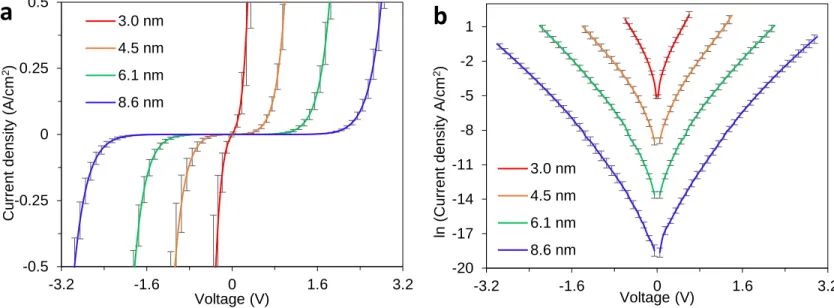
As reported previously, relative standard deviations (RSD) for the current density measured for a series of independent molecular junctions made with the procedures outlined above are in the range of 10-30%. 2, 5, 6 JV curves for MJs with four different thicknesses of Fluorene in linear and semilogarithmic scale are shown in Figure S5 panel a and panel b, respectively. Error bars are standard deviations of current density for four measured junctions on a given chip shown in Figure S3.
Figure S5. (a) JV curves for different fluorene thicknesses, with each curve representing the
average of four junctions on a single sample. Yield for tested junctions was 100% of nonshorted junctions and error bars represent ± standard deviation for four junctions of each thickness. (b) Semilogarithmic plot of JV curves shown in panel a.
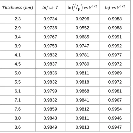
3 Linearity of lnJ for Fluorene devices with various abscissas
The JV curves for fluorene MJs shown in Figure 2 and 3 of the main text were subjected to linear least square fits for plots of ln J vs V, ln (J/V) vs V1/2 and ln J vs V1/2
-20 -17 -14 -11 -8 -5 -2 1 -3.2 -1.6 0 1.6 3.2 ln (Cur ren t de ns ity A /c m 2) Voltage (V) 3.0 nm 4.5 nm 6.1 nm 8.6 nm -0.5 -0.25 0 0.25 0.5 -3.2 -1.6 0 1.6 3.2 Cur ren t de ns ity ( A /c m 2) Voltage (V) 3.0 nm 4.5 nm 6.1 nm 8.6 nm
a
b
9
for all thirteen FL thicknesses, yielding the correlation coefficients (𝑅2) cited in the main text and listed in Table S2.
Table S2: R2 for Fluorene data shown in Figure 2b of the main text, following least square fit to the abscissa indicated.
As it is apparent from Table S2, 𝑙𝑛𝐽 vs 𝑉1/2 functional form for all thicknesses have the
best (highest) 𝑅2. The resulting slopes and intercepts for the case of 𝑙𝑛𝐽 vs 𝑉1/2 are provided in table S3. 𝑇ℎ𝑖𝑐𝑘𝑛𝑒𝑠𝑠 (𝑛𝑚) 𝑙𝑛𝐽 𝑣𝑠 𝑉 ln (𝐽⁄ ) 𝑣𝑠 𝑉𝑉 1/2 𝑙𝑛𝐽 𝑣𝑠 𝑉1/2 2.3 0.9734 0.9296 0.9988 2.9 0.9736 0.9552 0.9988 3.4 0.9767 0.9685 0.9991 3.9 0.9753 0.9747 0.9992 4.1 0.9832 0.9781 0.9977 4.5 0.9837 0.9780 0.9972 5.0 0.9836 0.9811 0.9969 5.5 0.9832 0.9818 0.9972 6.1 0.9799 0.9868 0.9981 7.1 0.9832 0.9841 0.9967 7.6 0.9859 0.9812 0.9954 8.0 0.9843 0.9811 0.9946 8.6 0.9849 0.9813 0.9947
10
Table S3: Slopes and intercepts for plots of lnJ vs V1/2 for Fluorene MJs
Thickness (nm) Intercept (b) Slope (a) 𝑅2
2.3 -4.45 10.623 0.9985 3.0 -6.40 10.668 0.9984 3.4 -7.74 10.584 0.9989 3.8 -9.46 10.788 0.9991 4.1 -10.58 11.233 0.9977 4.5 -11.74 11.234 0.9972 5.0 -13.55 11.633 0.9969 5.5 -15.19 11.838 0.9972 6.1 -16.91 11.995 0.9981 7.1 -19.43 12.267 0.9967 7.6 -20.79 12.699 0.9954 8.0 -21.62 12.614 0.9946 8.6 -22.70 12.970 0.9947
4 UV-Vis absorption spectra of molecular layers
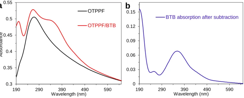
Polished quartz wafers (Technical Glass Products, Inc.) were diced into 1.8 x 1.2 cm chips to serve as substrates. The details for fabrication of optically transparent PPF (OTPPF) is described elsewhere.7 Briefly, a commercially available photoresist (AZ-P4330-RS) was diluted (12 % by volume) using propylene glycol methyl ether acetate, then this solution was spin coated onto quartz slides at 6000 rpm for 60 sec. The slides were pyrolyzed in a 1-inch tube furnace by heating under a flow of forming gas (5% H2, balance N2) to 1050 °C for 1 hour. All UV-Vis absorption spectra were obtained with a Perkin-Elmer Lambda 1050 dual beam spectrometer. The absorption spectra of the optically transparent PPF (OTPPF) films were then obtained, with a typical result shown in Figure S6-a, black curve. The same OTPPF substrate was then modified with molecular layers
11
with different thickness. Procedure for grafting molecular layer is the same as described in section 1.2. An example of the absorbance spectrum obtained for a layer of BTB on OTPPF is shown in Figure S6-a, red curve. Figure S6-b shows the subtraction of the unmodified OTPPF spectrum from the red curve of 6a, to clearly show the absorbance of the BTB molecular layer. The same procedure was used for all other molecules and UV-Vis shown in main text and below.
Figure S6. (a) UV-Vis absorption spectra for optically transparent PPF (black) and OTPPF
modified with a BTB layer (red). (b) OTPPF/BTB spectrum after subtraction of unmodified OTPPF spectrum.
For comparison of the UV-Vis results for the monomer of the molecules in the solution, Figure S7 shows spectra for AQ, BTB, FL, and NAB monomer in acetonitrile. Main peaks are indicated in the Figure and they can be compared to the numbers in Figure 5d and Table 1 in the main text.
0.3 0.35 0.4 0.45 0.5 0.55 190 290 390 490 590 A bs orbanc e Wavelength (nm) OTPPF OTPPF/BTB 0 0.03 0.06 0.09 0.12 0.15 190 290 390 490 590 Wavelength (nm)
BTB absorption after subtraction
12
Figure S7. UV-Vis absorption spectra for the indicated monomeric molecules in acetonitrile
solution, with concentrations near 1 x 10⁻⁴ M. Spectra were normalized to their absorbance maxima to permit comparison.
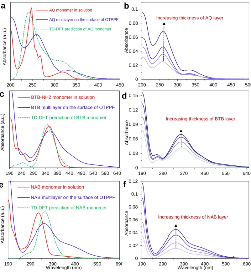
For comparison to the UV-Vis results for Fluorene in Figure 5a of the main text, Figure S8-a, c and e show overlays of monomer in solution, multilayer on OTPPF, and TD-DFT spectra for AQ, BTB, and NAB, respectively. Figure S8-b, d and f show how the absorbance of the grafted molecule on the surface of OTPPF change with increasing the thickness of the molecular layer.
0
0.2
0.4
0.6
0.8
1
1.2
220
260
300
340
380
420
460
500
N
orm
aliz
ed
abs
orbnc
e
(a.
u.
)
Wavelength (nm)
AQ
Fl
NAB
BTB-NH2
5.00 eV
4.73 eV
3.78 eV
3.49 eV
13
Figure S8. Overlays of UV-Vis spectra of molecule’s monomer in solution (ACN), multilayer on
OTPPF, and TD-DFT (B3LYP 6-31G) spectra for (a) AQ, (c) BTB, and (e) NAB. The optical absorbance of the grafted molecules on the surface of OTPPF with increasing molecular layer thickness for (b) AQ, (d) BTB, and (f) NAB.
0 0.02 0.04 0.06 0.08 0.1 200 250 300 350 400 450 500 A bs orbanc e
Increasing thickness of AQ layer
200 250 300 350 400 450 A bs orbanc e (a.u .) AQ monomer in solution
AQ multilayer on the surface of OTPPF
TD-DFT prediction of AQ monomer 0 0.03 0.06 0.09 0.12 0.15 190 280 370 460 550 640 A bs orbanc
e Increasing thickness of BTB layer
190 240 290 340 390 440 490 540 590 640 A bs orbanc e (a.u .) BTB-NH2 monomer in solution
BTB multilayer on the surface of OTPPF TD-DFT prediction of BTB monomer 190 290 390 490 590 690 A bs orbanc e (a.u .) Wavelength (nm)
NAB monomer in solution
NAB multilayer on the surface of OTPPF TD-DFT prediction of NAB monomer
0 0.02 0.04 0.06 0.08 0.1 0.12 190 290 390 490 590 690 A bs orbanc e Wavelength (nm)
Increasing thickness of NAB layer
b
a
c
d
14 5. JV curves for NAB, AQ and BTB
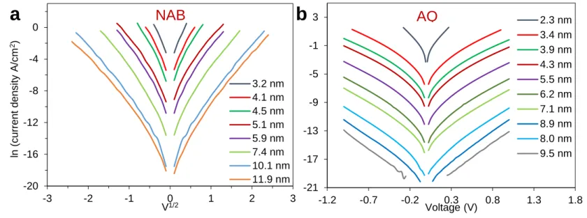
AQ and NAB junctions in a range of ~ 2 to 11 nm are fabricated to be compared with FL junctions. Figure S9-a and -b shows JV curves in semilogarithmic scale for NAB and AQ, respectively. The JV curves of BTB junctions were reported previously 4.
Figure S9. JV curves in semilogarithmic scale for different thicknesses of (a) NAB, (b) AQ.
The direct comparison between different molecules is shown in Figure S10. lnJ is plotted
vsV1/2 for four molecules in a range of ~ 2 to 11 nm. For all thicknesses and molecules are shown in the Figure S10, 𝑅2 values are better than 0.99.
-20 -16 -12 -8 -4 0 -3 -2 -1 0 1 2 3 ln (c urr en t d en s ity A /c m 2) V1/2 3.2 nm 4.1 nm 4.5 nm 5.1 nm 5.9 nm 7.4 nm 10.1 nm 11.9 nm -21 -17 -13 -9 -5 -1 3 -1.2 -0.7 -0.2 0.3 0.8 1.3 1.8 Voltage (V) 2.3 nm 3.4 nm 3.9 nm 4.3 nm 5.5 nm 6.2 nm 7.1 nm 8.9 nm 8.0 nm 9.5 nm
NAB
AQ
a
b
15
Figure S10. lnJ vs V1/2 for different thicknesses of (a) BTB, (b) NAB, (c) AQ, (d) FL.
-20 -15 -10 -5 0 0.1 0.45 0.8 1.15 1.5 1.85 ln(c urr en t de ns ity A /c m 2) V1/2 2.3 nm 3.4 nm 3.9 nm 4.3 nm 5.5 nm 6.2 nm 7.1 nm 8.0 nm 8.9 nm 9.5 nm 10.6 nm -20 -16 -12 -8 -4 0 0.15 0.55 0.95 1.35 1.75 V 1/2 2.3 nm 2.9 nm 3.4 nm 3.9 nm 4.1 nm 4.5 nm 5.0 nm 5.5 nm 6.1 nm 7.1 nm 7.6 nm 8.6 nm -20 -15 -10 -5 0 0.25 0.6 0.95 1.3 1.65 2 ln (c urr en t d en s ity A /c m 2) V1/2 4.5 nm 5.2 nm 6.9 nm 8.1 nm 10.4 nm 12.8 nm -21 -16 -11 -6 -1 0.25 0.6 0.95 1.3 1.65 2 V1/2 3.2 nm 4.1 nm 4.5 nm 5.1 nm 5.9 nm 7.4 nm 10.1 nm 11.9 nm
BTB
NAB
AQ
FL
d
c
a
b
16 6. Temperature dependent experiments
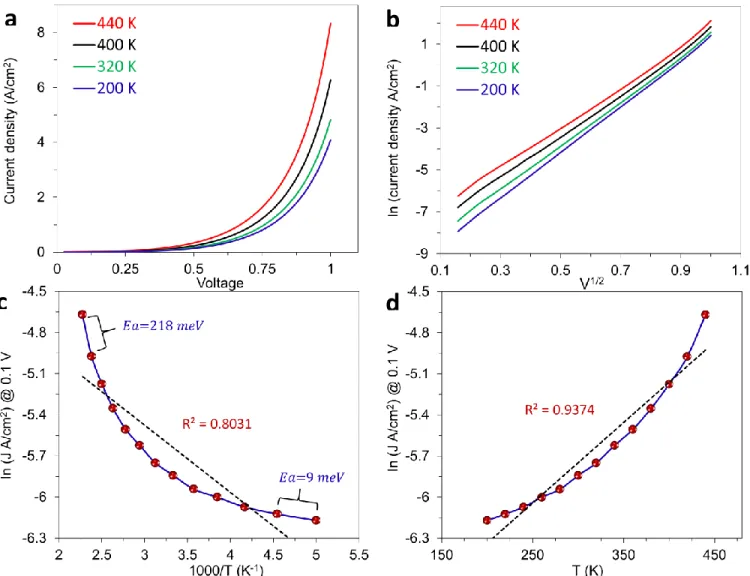
The similar analysis to Figure 4 of the main text for two other thicknesses of Fluorene junctions (3.8 and 7.6 nm) is shown in the Figure S11 and S12.
Figure S11. (a) JV curves for PPF/FL3.8/eC10/Au20 junction at four temperatures from 200 to 440 K in vacuum. (b) ln J vs V1/2 plots for curves in panel a. (c) Arrhenius plots at 0.1, with apparent activation energies for high and low T segments. (d) ln J vs T at 0.1 V. R2 for linear fits of the lines are indicated.
a
c
b
d
17
Figure S12. (a) JV curves for PPF/FL7.6/eC10/Au20 junction at four temperatures from 200 to 440 K in vacuum. (b) ln J vs V1/2 plots for curves in panel a. (c) Arrhenius plots at 0.1, with apparent activation energies for high and low T segments. (d) ln J vs T at 0.1 V. R2 for linear fits of the lines are indicated.
Apparent activation energies in different thickness, applied voltage bias and temperature range for Fluorene junctions are listed in Table S4.
a
b
d
c
18
Table S4: Apparent activation energies for Fluorene junctions
Thickness Voltage 𝐸𝑎 𝑚𝑒𝑉 (200 − 220 𝑇) 𝐸𝑎 𝑚𝑒𝑉 (280 − 300 𝑇) 𝐸𝑎 𝑚𝑒𝑉 (360 − 380 𝑇) 𝐸𝑎 𝑚𝑒𝑉 (420 − 440 𝑇) 3.8 nm 0.1 V 8.8 33.1 83.2 218.1 0.5 V 3.5 17.2 64.3 161.0 1.0 V 2.8 15.3 39.1 142.4 5.5 nm 0.1 V 8.5 28.9 61.0 133.1 0.5 V 5.7 22.7 37.9 110.7 1.0 V 3.7 14.7 36.6 110.5 1.5 V 0.54 14.8 40.1 140.3 7.6 nm 0.1 V 13.0 83.9 186.5 408.1 0.5 V 42.9 43.4 67.8 423.5 1.0 V 21.2 68.9 166.3 352.5 1.5 V 14.7 54.7 139.0 398.7 2.0 V 10.7 57.5 104.1 420.3 2.5 V 0 26.1 60.4 323.6
In order to have a direct comparison in temperature dependence between different thicknesses of Fluorene junction, Figure S13 shows the overlay of ln J vs Temperature for 3.8, 5.5 and 7.6 nm of Fluorene molecular layer at 𝑉 = 0.1 V.
19
Figure S13. ln J vs T at 0.1 V for fluorene junction at different thickness. Slopes and intercepts
for linear fits of the lines are indicated.
ln J vs Temperature for BTB and AQ at constant voltage with different thicknesses are shown in the Figure S14.
Figure S14. (a) lnJ vs T for AQ junctions at indicated thickness and voltage (b) ln J vs T for BTB
at indicated thickness and voltage -13 -11.5 -10 -8.5 -7 -5.5 250 300 350 ln ( curr en t de nsi ty A /cm 2) T (K) 11 nm @ 1.65 V 7.5 nm @ 0.4 V 5.5 nm @ 0.2 V 4.0 nm @ 0.1 V
AQ
-3 -2.5 -2 -1.5 -1 -0.5 0 0.5 180 230 280 330 380 T (K) 8.1 nm @ 1.5 V 10.4 nm @ 1.5 VBTB
y = 0.0127x - 17.2 y = 0.0062x - 11.2 y = 0.0059x - 7.5 -16 -14 -12 -10 -8 -6 -4 120 220 320 420 520 ln (J A/cm 2 ) @ 0.1 V T (K) 3.8 nm 5.5 nm 7.6 nma
b
20 7. Schottky and Poole-Frenkel mechanisms
Linearity of lnJ with V1/2 in a wide range of applied voltage is apparent from Figure S10 for four molecules at different thicknesses. This behavior is often associated with Schottky emission at interfaces or Poole-Frankel transport between coulombic “traps”. Schottky and Pool-Frankel are field dependent charge transport mechanisms, in a sense that at constant field for different thicknesses of the molecular layer, there should be constant conductivity. Figure S15-a shows lnJ of Fluorene junctions versus E1/2 for a range of thicknesses. The lines are not parallel anymore like Figure 3 in the main text and Figure S10 but still, they don’t converge to the single line. In order to make it clear, Figure S15-b shows the corresponding attenuation plot at constant applied field.
Figure S15. (a) ln J vs E1/2 plots for curves for Fluorene junctions with thickness indicated in nm. (b) Attenuation plot at the constant field for the line shown in panel a at 𝐸 = 0.25, 1 and 2 V/nm, with the slopes (β) indicated.
It is apparent from the Figure S15-b that there is an exponential dependence between current density and thickness at the constant field, and the attenuation slope (β) is field
-21 -17 -13 -9 -5 -1 3 0 0.1 0.2 0.3 0.4 0.5 0.6 0.7 ln (Cur ren t de ns ity A /c m 2) E1/2 2.3 2.9 3.4 3.9 4.1 4.5 5 5.5 6.1 7.1 8.6 -20 -16 -12 -8 -4 0 4 1 2.5 4 5.5 7 8.5 10 ln J @ c on s tan t fi el d
Molecular layer thickness (nm)
β= 1.87 nm-1 @ 1 V/nm
β= 1.34 nm-1 @ 2 V/nm
β= 2.42 nm-1 @ 0.25 V/nm
21
dependent. With attention to the equation 1 and 2 for Schottky emission and P-F mechanism, it means that the barrier height (𝜙0)and dielectric constant(𝜀) are changing with thickness: Schottky equation:
𝑙𝑛𝐽 = 𝑙𝑛𝐴𝑇2− (𝜙0−( 𝑞 4𝜋𝜀𝜀0) 1 2⁄ 𝑘𝑇 ) 𝐸 1/2
(eq 1) Pool-Frankel equation: ln (𝐽⁄ ) = 𝑙𝑛𝑁𝐸 0𝑞𝜇 − (𝜙0−( 𝑞 𝜋𝜀𝜀0) 1/2 𝑘𝑇 ) 𝐸 1/2 (eq 2)
Where, 𝐴 is the Richardson constant, 𝜙0barrier height, 𝜀0 the permittivity of vacuum, 𝑘 the Boltzmann constant, and 𝑞 the electron charge. 𝜇 and 𝑁0 are the mobility of carrier and the number of traps at zero field, and they are assumed constant at 1 × 10⁻⁶ cm/V.s and
1 × 10¹⁷ e/cm3, respectively. The fitting was done with two variable, barrier height (𝜙
0)
and dielectric constant (𝜀). The obtained values from the fitting of Schottky and Pool-Frankel are listed in Table S5 and S6, respectively.
Table S5. Parameters obtained by fitting of Pool-Frankel mechanism to experimental data.
Thickness (nm) Barrier height 𝜙0 (eV) Dielectric constant (ϵ) R2 Activation energy (𝐸𝑎 𝑚𝑒𝑉) b @ 0.1 𝑉 @ 0.5 𝑉 @ 1.0 𝑉 2.3 -0.04 78.86 0.9296 -104 a -152 a -189 a 2.9 0.01 47.30 0.9552 -61 a -117 a -158 a 3.4 0.03 59.48 0.9685 -26 a -92 a -141 a 3.9 0.07 45.03 0.9753 16 -56 a -110 a 4.1 0.12 28.94 0.9781 50 -36 a -100 a 4.5 0.14 28.43 0.9781 72 -11 a -73 a 5.0 0.23 15.10 0.9801 143 35 -46 a 5.5 0.23 18.83 0.9818 154 62 -7 a
22
a When the barrier height is small, even low applied bias can make the sign of effective barrier
height negative in Pool-Frankel equation, which obviously doesn’t have physical meaning.
b Activation energies are calculated based on the fitted barrier height and dielectric constant.
Table S6. Parameters obtained by fitting of Schottky mechanism to experimental data
a Activation energies are calculated based on the fitted barrier height and dielectric constant
6.1 0.28 15.33 0.9868 198 101 28 7.1 0.34 12.24 0.9841 258 157 82 7.6 0.38 10.51 0.9810 288 183 104 8.0 0.40 9.53 0.9800 316 208 128 8.6 0.42 8.59 0.9813 334 225 143 Thickness (nm) Barrier height ϕ0 (eV) Dielectric constant (ϵ) 𝑅2 Activation energy (𝐸𝑎 𝑚𝑒𝑉) a @ 0.1 𝑉 @ 0.5 𝑉 @ 1.0 𝑉 2.3 0.54 8.21 0.9988 447 339 258 2.9 0.59 6.79 0.9988 497 389 308 3.4 0.62 5.68 0.9991 532 425 345 3.9 0.66 4.90 0.9992 574 466 384 4.1 0.69 4.16 0.9977 600 487 402 4.5 0.72 3.80 0.9972 630 517 432 5.0 0.77 3.19 0.9801 674 556 468 5.5 0.81 2.79 0.9969 714 595 505 6.1 0.86 2.45 0.9972 758 636 546 7.1 0.92 2.03 0.9967 820 696 604 7.6 0.96 1.76 0.9954 852 724 628 8.0 0.98 1.69 0.9946 874 747 651 8.6 1.00 1.49 0.9947 899 768 670
23
Apart from the physically unreasonable values of fitted barrier height and dielectric constant, the trend of changing parameters with thickness could be more important. The fitting analysis shows the significant decrease in dielectric constant with increasing thickness for both P-F and Schottky mechanism. Dielectric constant for the Fluorene junctions were measured experimentally by means of impedance spectroscopy. The result shown in Figure S16, indicate opposite trend for changing dielectric constant with thickness.
Figure S16. Dielectric constant measured by impedance spectroscopy for Fluorene junctions
versus thickness of Fluorene molecular layer.
From the wide range of barrier heights and dielectric constants required to fit the experimental results to either Schottky or Poole-Frenkel mechanisms, we conclude that these mechanisms are invalid for the carbon-based aromatic devices discussed in this report.
y = 0.59 x + 1.27
2.5 3.5 4.5 5.5 6.5 2.5 3.5 4.5 5.5 6.5 7.5 8.5 Dielectric constan t Thickness (nm)24 References:
1. Ru, J.; Szeto, B.; Bonifas, A.; McCreery, R. L. Microfabrication and Integration of Diazonium-Based Aromatic Molecular Junctions. ACS Appl. Mater. Interfaces 2010, 2, 3693-3701. 2. Sayed, S. Y.; Fereiro, J. A.; Yan, H.; McCreery, R. L.; Bergren, A. J. Charge Transport in Molecular Electronic Junctions: Compression of the Molecular Tunnel Barrier in the Strong Coupling Regime. Proc. Natl. Acad. Sci. 2012, 109, 11498-11503.
3. Anariba, F.; DuVall, S. H.; McCreery, R. L. Mono- and Multilayer Formation by Diazonium Reduction on Carbon Surfaces Monitored with Atomic Force Microscopy "Scratching". Anal. Chem. 2003, 75, 3837-3844.
4. Yan, H.; Bergren, A. J.; McCreery, R.; Della Rocca, M. L.; Martin, P.; Lafarge, P.; Lacroix, J. C. Activationless Charge Transport across 4.5 to 22 Nm in Molecular Electronic Junctions. Proc. Natl. Acad. Sci. 2013, 110, 5326-5330.
5. Morteza Najarian, A.; Szeto, B.; Tefashe, U. M.; McCreery, R. L. Robust All-Carbon Molecular Junctions on Flexible or Semi-Transparent Substrates Using "Process-Friendly" Fabrication. ACS Nano 2016, 10, 8918-8928.
6. Yan, H.; Bergren, A. J.; McCreery, R. L. All-Carbon Molecular Tunnel Junctions. J. Am. Chem. Soc. 2011, 133, 19168-19177.
7. Tian, H.; Bergren, A. J.; McCreery, R. L. Ultravioletvisible Spectroelectrochemistry of Chemisorbed Molecular Layers on Optically Transparent Carbon Electrodes. Appl. Spectrosc. 2007, 61, 1246-1253.