KxNa1-xNbO3 perovskite thin films grown by pulsed laser deposition
on R-plane sapphire for tunable microwave devices
B. Aspea,b, F. Cisséa,b, X. Castelb, V. Demangea, S. Députiera, S. Olliviera, V. Bouqueta, L. Joannyc, R. Sauleaub, M. Guilloux-Virya,c
a
Univ Rennes, CNRS, ISCR – UMR 6226, F-35000 Rennes, France
b
Univ Rennes, CNRS, IETR – UMR 6164, F-35000 Rennes, France
c
Univ Rennes, CNRS, ScanMAT - UMS 2001 F-35000 Rennes, France
corresponding authors:
Barthélemy Aspe: email adress: barthelemy.aspe@univ-rennes1.fr
ORCID identifier: 0000-0001-8927-4013 phone number: +33 (0) 2 23 23 65 70
Maryline Guilloux-Viry: email adress: maryline.guilloux-viry@univ-rennes1.fr ORCID identifier: 0000-0001-7773-1643
phone number: +33 (0) 2 23 23 56 55
Abstract
KxNa1-xNbO3 thin films with x = 0.5 and x = 0.7 were deposited by pulsed laser deposition
onto R-cut sapphire substrates to be suitable for microwave applications. The 500-800 nm-thick films present a preferential (100) orientation. The ω-scans show a weak mosaicity (full-width-at-half-maximum equal to 0.36° and 0.60° for x = 0.5 and x = 0.7, respectively). In addition to this texture, the in-plane ordering evidenced by X-ray diffraction φ-scan for the (100) orientation is in agreement with an epitaxial-like growth in spite of the high lattice mismatch between KxNa1-xNbO3
and sapphire. The dielectric characteristics and the frequency tunability at microwave frequencies were obtained from coplanar waveguide devices (transmission lines and stub resonators). For the K0.5Na0.5NbO3 and K0.7Na0.3NbO3 compositions, high dielectric permittivity εr values of 360 and
250, and loss tangent tanδ values of 0.36 and 0.43 without biasing were retrieved from the transmission lines measurements at 10 GHz, respectively. Frequency tunabilities of 15 % and 12 % have been assessed under 80 kV/cm biasing from stub resonator measurements for the K0.5Na0.5NbO3 and K0.7Na0.3NbO3 compositions, respectively. K0.5Na0.5NbO3 composition is
therefore a promising solution for miniaturized tunable devices at microwave frequencies.
Keywords: ferroelectrics; thin films; tunable devices; microwave frequencies.
1. Introduction
From the last decade, a great interest is devoted to multifunctional oxides that present a wide range of properties, and offer new opportunities in the development of efficient devices. In this frame, ferroelectric materials, which exhibit also piezoelectric behavior, have been extensively studied due to their numerous applications in sensors, micro-electro-mechanical systems (MEMS) and memory devices [1–4]. Nowadays, wireless applications require advanced miniature and tunable microwave devices [5–7]. Besides the standard reconfigurable devices based on radiofrequency micro-electro-mechanical systems (RF-MEMS) or solid-state components, integration of ferroelectric materials brings an alternative solution. Indeed ferroelectric thin films exhibit a high dielectric permittivity εr which can be controlled by an external static electric field,
promoting both miniaturized and reconfigurable microwave devices. Besides the most popular ferroelectric materials, namely BaxSr1-xTixO3 (BST) [8, 9] and PbZr1-xTixO3 (PZT) [10, 11], the
lead-free potassium niobate family presents relevant features [12–14].
Currently, among the lead-free ferroelectric materials, a specific attention is paid to the perovskite-type oxide KxNa1-xNbO3 (KNN). The KNN compositions belong to a solid solution
between the ferroelectric KNbO3 (orthorhombic, space group (SG): Bmm2, JCPDS file #
01-071-2171) and the antiferroelectric NaNbO3 (orthorhombic, SG: P21ma, JCPDS file # 01-077-0873)[15,
16]. Through the solid-solution, the KNN compounds present various crystalline symmetries. Only 2
2 % atomic of K is sufficient to modify the structure of NaNbO3 [17]. At room temperature, for x
lying between 0.48 and 0.83, the KNN compounds have a primitive monoclinic cell with am ≈ cm ≈
4 Å > bm, and β slightly higher than 90°. The phases can also be described by a larger A-centered
orthorhombic cell (i.e. a0 ≈ c0 ≈ 4√2 Å) [18, 19]. Tellier et al. and Handoko et al. have shown that
the lattice parameters am and cm increase with the potassium content. This increase is explained by
the larger K+ radius (1.33 Å) against the Na+ one (0.97Å) [18, 19].
The KNN oxide exhibits (i) high Curie temperature (Tc≈ 400°C) depending upon its
composition [17, 20], (ii) high values of dielectric permittivity εr (between 100 and 500 at 100 kHz
[15]), and (iii) high piezoelectric coefficient d33 (up to 300 pC/N [21]). This range in Tc value is
valuable to ensure the strong thermal stability of the targeted microwave devices operating at room temperature. Recent studies were reported at microwave frequencies on KNN ceramics and thin films [22–26]. As expected, the dielectric permittivity varies according to the bulk composition from εr = 92 for K0.2Na0.8NbO3 to εr = 124 for K0.5Na0.5NbO3 at 10 GHz [23]. On one hand,
Peddigari et al. reported values of εr = 287 and loss tangent tanδ = 0.01 at 10 GHz on
K0.5Na0.5NbO3 thin films [25]. On the other hand, Kim et al. reported the value tanδ = 0.23 at
20 GHz on K0.5Na0.5NbO3 thin films (εr value not available) with a capacitance tunability of 22 % at
20 GHz under an external biasing field Ebias = 200 kV/cm [26]. According to these preliminary
studies, compositions with the lowest potassium/sodium ratio are not identified as promising candidates for microwave applications. This explains why the K0.5Na0.5NbO3 composition has been
first selected here. Moreover, its proximity with the reported morphotropic phase boundary [27], defined as continuous-phase transitions between two crystalline structures, augurs well for interesting ferroelectric properties at microwave frequencies [28]. A second composition with a higher potassium/sodium ratio (K0.7Na0.3NbO3)has also been studied here.
The main objective of the present work is to investigate the microwave response of tunable devices based on KNN thin films. Two compositions K0.5Na0.5NbO3 and K0.7Na0.3NbO3 were
investigated in detail. The microstructure and the crystalline characteristics of the thin films grown by pulsed laser deposition on R-plane sapphire substrates were determined and the related KNN-based tunable device performances at microwave frequencies were compared.
2. Experimental details
2.1. Elaboration of KNN thin films by pulsed laser deposition (PLD)
The ceramic targets were prepared from KNN powders first synthesized by a solid state reaction at 940°C for 4 hours in air from sodium carbonate Na2CO3 (RP NORMAPUR 99.8%), anhydrous
potassium carbonate K2CO3 (ACROS Organics 99 %) and niobium oxide Nb2O5 (Alfa Aesar
99.5%) powders mixed in a planetary ball-mill for 1 hour at a 400 rotations per minute speed (PM100, Retsch). In a second step, the powders were K-enriched with a potassium nitrate KNO3
powder, to balance the loss of potassium during the laser deposition due to its volatility. Afterwards the powders were uniaxially pressed into 25 mm-diameter targets and annealed up to 500°C in air for 3 hours.
The KNN thin films were deposited by the pulsed laser deposition (PLD) technique from two KNN targets. By controlling the K/Na ratio of the home-made targets, two thin film compositions were prepared: K0.5Na0.5NbO3 (KNN50/50) and K0.7Na0.3NbO3 (KNN70/30). Each thin film was
grown on R-plane sapphire (11�02) Al2O3 (10 mm × 10 mm × 0.5 mm) single crystal previously
cleaned in acetone and isopropanol ultrasonic baths for 5 min each. Despite the strong mismatch with the perovskite-like structures, sapphire substrate fits well within microwave applications, thanks to its convenient dielectric characteristics (εr ≈ 10 and tanδ ≈ 10-4 at 10 GHz and room
temperature). Moreover sapphire substrate is highly stable in air and moisture atmosphere, then well suitable for further lithography and wet etching processes. A KrF excimer laser (Coherent company, pulse duration 20 ns, λ=248 nm) set at an energy of 210 mJ, a fluence of 2-3 J.cm-2 and a 4 Hz working frequency, was used to ablate the KNN ceramic targets. The KNN films were grown onto
sapphire substrates heated at 650°C and located at 55 mm in front of the selected target, under a 0.3 mbar oxygen pressure. The expected deposition rate being close to 15 nm/min, a deposition time of 40 minutes was used to obtain a thin film thickness of about 600 nm.
2.2. KNN thin film characterizations
The structural characteristics were investigated by X-ray diffraction (XRD) by using a
θ−2θ diffractometer (D8 Advance, BRUKER) with a monochromatized Cu Kα1 wavelength
(λ=1.54056 Å) and a texture diffractometer (D8 Discover, BRUKER) giving access to the θ−2θ, ω-scan and ϕ-ω-scan modes. The surface morphology was observed at 10 kV by ω-scanning electron microscopy (SEM, JSM 7100F, JEOL) coupled with an energy dispersive X-ray spectroscopy detector (EDS, SDD X-Max 50mm2, Oxford Instruments) to determine the thin film composition. A 5 nm–thick carbon layer was deposited before SEM observation to ensure optimal element detection and especially the potassium element detection that we have observed to be highly sensitive to charge accumulation effect. Each film thickness was measured by SEM on a transverse section obtained from a fracture along an edge.
2.3. KNN microwave devices
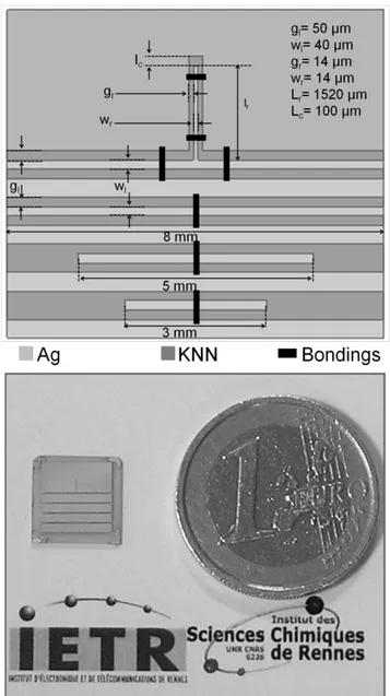
The dielectric characteristics and the frequency tunability of the KNN thin films were investigated using coplanar waveguide (CPW) devices designed with a 3-D commercial electromagnetic software (Ansys HFSSTM). Three 50-Ω transmission lines (8 mm, 5 mm and 3 mm long) with a width wl = 40 µm surrounded by a gap gl = 50 µm (Figure 1) were implemented to
retrieve the KNN dielectric characteristics, namely the dielectric permittivity εr and the loss tangent
tanδ, from the microwave measurements. A CPW quarter-wavelength open-ended stub resonator was also designed to operate in X-band (Figure 1). Its resonance frequency Fr depends upon the
stub length Lr and the effective permittivity εeff of the heterostructure, as follows:
𝐹𝐹
𝑟𝑟=
4𝐿𝐿𝑟𝑟�𝜀𝜀𝑐𝑐 𝑒𝑒𝑒𝑒𝑒𝑒(1) where c is the speed of light in vacuum. The devices were fabricated from a 2 µm-thick silver overlayer / 5 nm-thick titanium underlayer deposited by RF magnetron sputtering at room temperature. The silver thickness is three times larger than the skin depth value (δ = 0.64 µm) at 10 GHz. Note that the ultra-thin titanium film is used here only to ensure the strong adhesion of the silver metallization onto the ferroelectric oxide. Standard photolithography and wet etching processes were implemented to pattern the devices. Gold wire bondings (15 µm-diameter and 250 µm-length) were used to enforce the equipotential condition on both CPW grounds and prevent from the excitation of parasitic slotline mode.
Microwave measurements at room temperature were carried out through a probe station coupled to a vector network analyzer (VNA 8510C, Hewlett Packard) from 1 GHz to 20 GHz under an external DC bias voltage range from 0 V to 150 V, which corresponds to a maximal static electric field Ebias equal to 80 kV/cm for the stub resonator and 27 kV/cm for the transmission lines.
The measured gap dimensions (gr ≈ 18 µm and gl ≈ 54 µm) are slightly larger than the nominal ones
(Figure 1) due to the inherent overetching of the wet etching process used. Further details are reported elsewhere [29].
Fig. 1 Layout, dimensions and picture of the CPW devices
3. Results and discussion
3.1. Composition, microstructure and structural properties of the KNN thin films
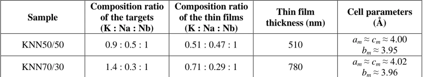
The volatility of potassium, which is higher than that of sodium [30], greatly influences the global stoichiometry of the thin films at the end of the deposition process. Consequently, as described in the experimental details section, the two home-made targets have been K-enriched. The EDS analyses of the targets and of the related thin films (Table 1) depict this volatility. Even after a strong enrichment of the target, the K0.5Na0.5NbO3 thin film may exhibit a slight lack of
alkaline elements with a ratio of (K+Na)/Nb typically in the range ∼ 0.95-1. This lack of alkaline elements may lead to an oxygen deficiency for charge compensation. The related oxygen vacancies may be responsible for decreasing the piezoelectric and dielectric properties in some ferroelectric oxides [31]. Here, the reported compositions are average values obtained from three measurements performed on different areas of each sample. The achievement of a standard deviation lower than 2% is affording evidence tending to prove the good homogeneity and reproducibility of the deposition method used. Nevertheless the overall accuracy of EDS technique itself is usually considered close to 10%, especially in the case of resistive materials in thin films. These results enable us to confirm the so-called KNN50/50 thin film composition close to K0.5Na0.5NbO3 and that
of the KNN70/30 thin film close to K0.7Na0.3NbO3.
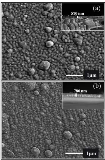
Figure 2 displays the regular morphology of the thin films. The homogeneous shape of the grains and their arrangement suggest a preferred orientation. Some outgrowths currently observed at the surface of thin films deposited by PLD, especially with not highly densified targets, are visible with a lateral size that is still submicronic. The KNN50/50 sample exhibits a thickness slightly lower than the targeted value: 510 nm against ∼ 600 nm (Figure 2a) in contrast with the KNN70/30 sample which presents a thickness equal to 780 nm (Figure 2b). The thickness difference between the two compositions has been systematically obtained with other samples (not shown here).
Sample
Composition ratio of the targets (K : Na : Nb)
Composition ratio of the thin films
(K : Na : Nb) Thin film thickness (nm) Cell parameters (Å) KNN50/50 0.9 : 0.5 : 1 0.51 : 0.47 : 1 510 am ≈ cm ≈ 4.00 bm ≈ 3.95 KNN70/30 1.4 : 0.3 : 1 0.71 : 0.29 : 1 780 am≈ cm≈ 4.02 bm≈ 3.96
Table 1 Composition, thickness and measured cell parameters of the thin films versus the target composition
Fig. 2 SEM images of the surface morphology and cross-sections (in inset) of (a) KNN50/50 and (b) KNN70/30 thin films
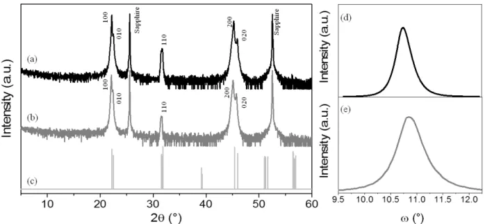
The XRD patterns of the KNN50/50 and KNN70/30 samples are depicted in Figures 3a and 3b using the monoclinic indexation and displayed with a logarithmic intensity scale. A powder XRD pattern available from the database (JCPDS file # 00-061-0315) is displayed as reference in Figure 3c [18]. It is worth noting that deficiency in alkaline elements often leads to the presence of the unwanted K4Nb6O17 phase (JCPDS file # 01-076-0977), leading to a peak at 2θ ≈ 10° on XRD
patterns [32]. For our samples, all the peaks are purely indexed in the KNN phase, demonstrating the absence of such secondary phases. The two peaks at 2θ ≈ 22° correspond to the diffraction of the (100) and (010) KNN planes. A strong (100) orientation is observed on both KNN50/50 and KNN70/30 films with a second weaker (110) orientation at 2θ ≈ 32°. The relative intensities of the (100), (010) and (110) peaks are similar for both samples. The orientation factors of the (100) peak,
computed by the Lotgering method [33], comparing the relative intensity of the peaks from the experimental XRD patterns (Figures 3a and 3b) to the powder XRD patterns available from the database, are equal to 0.93 and 0.90 for the KNN50/50 and KNN70/30 films, respectively. Therefore both samples can be considered as structurally alike. The slight shift of the KNN70/30 2θ peaks towards large angles is attributed to the lattice parameters increase with K amount increase in the compounds (Table 1). These results are in agreement with the cell parameter values reported by Tellier et al. and Hondoko et al. of am = 4.004 Å and cm = 3.944 Å for K0.5Na0.5NbO3,
and am = 4.01 Å and cm = 3.97 Å for K0.7Na0.3NbO3 [18, 19].
Fig. 3 Θ-2Θ X-ray diffraction patterns displayed with a logarithmic intensity scale of (a) KNN50/50 thin film, (b) KNN70/30 thin film (c) K0.5Na0.5NbO3 powder retrieved from the database JCPDS file
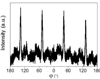
# 00-061-0315 [18]; ω-scans on the (100) peak of (d) KNN50/50 and (e) KNN70/30 thin films To further investigate the crystalline quality of the samples, ω-scans on the (100) peak (Figures 3d and 3e) were recorded. The full-width-at-half-maximum (FWHM) is equal to 0.36° and 0.60° for the KNN50/50 and KNN70/30 samples, respectively. Those values are a good indication of the well-textured thin films. The ω-scan on the (11�02) sapphire substrate gives FWHM = 0.02° for comparison. The φ-scans were also performed on the KNN {110} planes (Figure 4). They present four distinctive peaks at 90° apart from one another, which indicate an in-plane ordering
which refers to an epitaxial-like growth for this orientation, besides a significant background noise corresponding to the texture. This result is in good agreement with the microstructure previously observed by SEM (Figures 2a and 2b). Though examples of epitaxial growth of perovskite on sapphire exist [34, 35], such crystalline growth was unexpected due to the large mismatch between the KNN perovskite phase and the R-plane sapphire (∼14%) and, at our knowledge, has not been reported yet.
Fig. 4 φ-scans performed on the KNN {110} planes typical of KNN50/50 and KNN70/30 thin films deposited on sapphire substrate
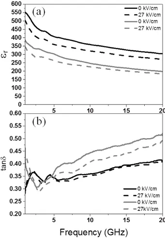
3.2. KNN dielectric characteristics
The dielectric characteristics (εr, tanδ) of the KNN thin films were retrieved from the
measured reflection (S11) and transmission (S21) coefficients of the CPW transmission lines (Figure
5) [29, 36]. Without biasing, KNN50/50 exhibits a permittivity value εr = 360 at 10 GHz against
250 for KNN70/30. Permittivity value of KNN50/50 is higher than those previously reported on Dy2O3-doped KNN thin films (εr = 307 at 10 GHz [37]) and on pure K0.5Na0.5NbO3 thin films
grown on Pt/Ti/SiO2/Si (εr = 287 at 10 GHz [25]). The higher permittivities measured in the present
study can be attributed to the crystalline orientation, i.e. epitaxial-like growth, of our samples, compared with the KNN polycrystalline growth mentioned by Peddigari et al. [25]. The loss is also
higher than that expected for this kind of materials: tanδ = 0.36 for KNN50/50 and tanδ = 0.43 for KNN70/30 without biasing at 10 GHz, whereas Peddigari et al. reported tanδ = 0.014 at 10 GHz for the Dy2O3-doped KNN thin films [37] and tanδ = 0.010 at 10 GHz for the annealed KNN thin films
[25]. As PLD technique induces outgrowths into KNN thin films (Figures 2a and 2b), the interface quality between the metallic transmission lines and the KNN films may have an impact on the retrieved tanδ values. This contribution to the measured loss, not present in the split post dielectric resonator (SPDR) [38] technique, could explain the tanδ values measured in the present study. Indeed our results can be compared with those reported by Kim et al. [26], i.e. tanδ = 0.23 at 20 GHz measured on a coplanar interdigitated capacitor. Under Ebias = 27 kV/cm, the dielectric
permittivity decreases from 360 to 320 for KNN50/50 and from 250 to 220 for KNN70/30 at 10 GHz, demonstrating the tunability of such compositions under biasing. The important decrease of the dielectric permittivity from 1 to 5 GHz with and without biasing is attributed to the freezing of the polar domain motion, whereas tanδ fluctuations in this frequency range are attributed in part to the metal skin depth loss [29].
Fig. 5 Measured frequency dependence of (a) dielectric permittivity εr and (b) intrinsic loss tanδ
with and without biasing; Black line: KNN50/50; Grey line: KNN70/30
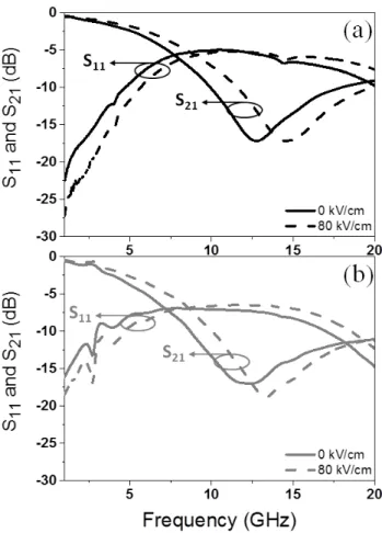
Resonance frequencies Fr (frequency value at the minimum S21, see Figure 6) of the CPW
stub resonators printed on the KNN50/50 and KNN70/30 samples were measured under various bias voltage values. The fine tuning of the KNN dielectric permittivity value under bias voltage controls Fr. The frequency tunability T (Figure 7) is computed from the Fr values under Ebias, as
follows:
𝑇𝑇(%) = |𝐹𝐹𝑟𝑟(𝐸𝐸𝑏𝑏𝑏𝑏𝑏𝑏𝑏𝑏=0)−𝐹𝐹𝑟𝑟(𝐸𝐸𝑏𝑏𝑏𝑏𝑏𝑏𝑏𝑏)|
𝐹𝐹𝑟𝑟(𝐸𝐸𝑏𝑏𝑏𝑏𝑏𝑏𝑏𝑏=0) × 100 (2)
The maximum external DC electric field applied is Ebias = 80 kV/cm. The shift of the resonance
frequency from 12.7 GHz (without biasing) to 14.6 GHz (Ebias max.) and from 12.0 GHz (without
biasing) to 13.4 GHz (Ebias max.) leads to a frequency tunability equal to 15% and 12% for the
KNN50/50 and KNN70/30 samples, respectively. More detailed results on tunability values under
various bias voltages are reported in Figure 7. Clearly the highest tunability is reached with the KNN50/50 sample, especially when the applied bias voltage is high.
Fig. 6 Measured reflection coefficient S11 and transmission coefficient S21 with and without biasing
on the stub resonator printed on (a) KNN50/50 and (b) KNN70/30
Fig. 7 Frequency tunability under biasing. KNN50/50; KNN70/30; the black and grey dotted lines are guide eyes
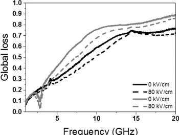
The global loss (GL) of the resonant devices was also computed from S11 and S21 magnitude
values at their specific resonance frequency Fr, as follows:
𝐺𝐺𝐺𝐺 = 1 − |𝑆𝑆11|2− |𝑆𝑆21|2 (3)
GL is plotted in Figure 8 from 1 to 20 GHz with and without Ebias for both samples. The computed
values without biasing for KNN50/50 (GL= 0.59) and KNN70/30 (GL= 0.76) are of the same order of magnitude, with a slightly higher value for KNN70/30. The decrease of GL under biasing (Table 2) is consistent with the related loss tanδ decrease for the KNN 70/30 sample. Regarding the KNN50/50 one, tanδ steadiness under biasing explains the non-variation of the GL.
Fig. 8 Global loss variation versus frequency with and without biasing; Black line: KNN50/50; Grey line: KNN70/30
Table 2 Dielectric permittivity εr, loss tangent tanδ, and tunability T of the KNN50/50 and
KNN70/30 samples at 10 GHz; global loss GL is computed at the stub resonator resonance frequency
An additional factor, other than composition, could induce the higher global loss exhibited by the KNN70/30 sample. Indeed, we have observed in a previous work that the use of a thicker ferroelectric film increases comparatively the global loss [39]. Therefore the global loss achieved on
Ebias = 0 kV/cm Ebias = 27 kV/cm Ebias = 80 kV/cm Ebias = 80 kV/cm
Sample εr tanδ GL εr tanδ GL T (%)
KNN50/50 360 0.36 0.59 320 0.35 0.51 15 KNN70/30 250 0.43 0.76 220 0.40 0.68 12
the 780 nm-thick KNN70/30 sample is consistent with that of the 510 nm-thick KNN 50/50. On the other hand, the frequency tunability is usually enhanced by a thicker film [39], contrasting with the results obtained here, which supports an effect due to the composition. The similar crystalline characteristics of both samples (see section §3.1) point also the discussion at the KNN composition itself. KNN50/50 with a composition close to the morphotropic phase boundary provides advanced performance, especially higher dielectric permittivity and higher frequency tunability at microwave frequencies (εr = 360 at 10 GHz and T = 15%). This value of tunability, while lower than that
reported by Kim et al. (T = 22% [26]) is relevant in regards to the moderate biasing used (Ebias =
80 kV/cm against 200 kV/cm in [26]). This tunability can also be compared with that reported in the KTaxNb1-xO3 (KTN) system, which from a chemical point of view, remains close to that of the KNN
system. Even though lower, the result is still relevant considering the KNN Curie temperature (Tc ≈
400°C) and therefore the greater thermal stability at room temperature that is expected. For comparison, the highest frequency tunability of the KTN-based devices (T = 44% under Ebias = 70
kV/cm at ∼10 GHz [29]) was obtained with a composition marked by a Curie temperature close to room temperature (Tc ≈ 90°C), improving thereby its reconfigurability but also its sensitivity to
temperature variation.
Nevertheless, some attempts need to be undertaken to decrease further KNN loss. Previous solutions have already been investigated on ferroelectric oxide materials, such as doping [40], crystalline quality improvement by the use of seed layer [41], extrinsic loss decrease by the use of ferroelectric/dielectric multilayers [42], as well as confining the ferroelectric layer in the efficient regions of the microwave devices [43].
4. Conclusion
This study presents the elaboration, the dielectric characterization and the performance at microwave frequencies of tunable ferroelectric KNN devices based on two compositions, namely
K0.5Na0.5NbO3 and K0.7Na0.3NbO3. It has been shown that structurally ordered thin films of KNN
perovskite on R-plane sapphire are achievable and greatly reproducible with different compositions using PLD technique. The highly oriented films with some in-plane order suggest an epitaxial-like growth, despite the strong mismatch between the two lattices (∼14%). The characterization of the KNN films at microwave frequencies demonstrates the higher performance at room temperature of the K0.5Na0.5NbO3 composition, close to the morphotropic phase boundary. A dielectric permittivity
εr = 360 at 10 GHz without biasing associated with a frequency tunability T = 15% under a
moderate bias voltage promotes the strong interest of such films as lead-free ferroelectric material for future tunable microwave devices.
5. Acknowledgment
The authors are grateful for the financial support of the Direction Générale de l’Armement (DGA) and the Région Bretagne (PhD research Grant of B.A, project ARMin). This work was also supported by the European Union through the European Regional Development Fund (ERDF), the Ministry of Higher Education and Research, the Région Bretagne, the Département des Côtes d’Armor and Saint-Brieuc Armor Agglomération, through the CPER Projects 2015-2020 MATECOM and SOPHIE / STIC & Ondes. ScanMAT, UMS 2001 CNRS-University of Rennes 1, received a financial support from the Région Bretagne, the Département d’Ille et Vilaine and the European Union (CPER-FEDER 2007–2014, Présage Nos. 39126 and 37339, and CPER SCANMAT 2015-2020). C. Derouet is warmly acknowledged for technical assistance for X-Ray diffraction.
6. References
1. Polla DL (1995) Microelectromechanical systems based on ferroelectric thin films. Microelectron Eng 29:51–58 . doi: 10.1016/0167-9317(95)00114-X
2. Muralt P (2000) Ferroelectric thin films for micro-sensors and actuators: a review. J Micromechanics Microengineering 10:136–146 . doi: 10.1088/0960-1317/10/2/307
3. Östling M, Koo S-M, Zetterling C-M, Khartsev S, Grishin A (2004) Ferroelectric thin films on silicon carbide for next-generation nonvolatile memory and sensor devices. Thin Solid Films 469–470:444–449 . doi: 10.1016/j.tsf.2004.09.030
4. Setter N, Damjanovic D, Eng L, Fox G, Gevorgian S, Hong S, Kingon A, Kohlstedt H, Park NY, Stephenson GB, Stolitchnov I, Taganstev AK, Taylor DV, Yamada T, Streiffer S (2006) Ferroelectric thin films: Review of materials, properties, and applications. J Appl Phys 100:051606 . doi: 10.1063/1.2336999
5. Chang K, Hsieh L-H (2004) Microwave ring circuits and related structures, 2nd ed. J. Wiley, Hoboken, N.J
6. Cruickshank DB (2011) Microwave materials for wireless applications. Artech House, Boston ; London
7. Petosa A (2012) An overview of tuning techniques for frequency-agile antennas. IEEE Antennas Propag Mag 54:271–296 . doi: 10.1109/MAP.2012.6348178
8. Gevorgian S (2009) Ferroelectrics in microwave devices, circuits and systems. Springer London, London
9. Li H-Y, Chen H-P, Chen S-C, Tai C-H, Fu J-S (2012) A tunable slot loop antenna using interdigitated ferroelectric varactors. Antennas and Propagation Society International Symposium (APSURSI), 2012 IEEE:1–2 . doi: 10.1109/APS.2012.6348537
10. Bedair SS, Pulskamp JS, Meyer CD, Mirabelli M, Polcawich RG, Morgan B (2012) High-performance micromachined inductors tunable by lead zirconate titanate actuators. IEEE Electron Device Lett 33:1483–1485 . doi: 10.1109/LED.2012.2207700
11. Qiu JX, Judy DC, Pulskamp JS, Polcawich RG, Kaul R, Crowne F (2009) Characterization of nonlinear behavior in a tunable phase shifter using ferroelectric PZT thin-film capacitors and its effect on system performance. Microwave Symposium Digest, 2009. MTT '09. IEEE MTT-S International:341–344 . doi: 10.1109/MWMTT-SYM.2009.5165703
12. Rödel J, Jo W, Seifert KTP, Anton E-M, Granzow T, Damjanovic D (2009) Perspective on the development of lead-free piezoceramics. J Am Ceram Soc 92:1153–1177 . doi: 10.1111/j.1551-2916.2009.03061.x
13. Li J-F, Wang K, Zhu F-Y, Cheng L-Q, Yao F-Z (2013) (K,Na)NbO3-based lead-free
piezoceramics: Fundamental aspects, processing technologies, and remaining challenges. J Am Ceram Soc 96:3677–3696 . doi: 10.1111/jace.12715
14. Wu J, Xiao D, Zhu J (2015) Potassium–sodium niobate lead-free piezoelectric materials: Past, present, and future of phase boundaries. Chem Rev 115:2559–2595 . doi: 10.1021/cr5006809 15. Egerton L, Dillon DM (1959) Piezoelectric and dielectric properties of ceramics in the system
potassium-sodium niobate. J Am Ceram Soc 42:438–442 . doi: 10.1111/j.1151-2916.1959.tb12971.x
16. Megaw HD, Wells M (1958) The space group of NaNbO3 and (Na0.995K0.005)NbO3. Acta
Crystallogr 11:858–862 . doi: 10.1107/S0365110X58002437 18
17. Ahtee M, Glazer AM (1976) Lattice parameters and tilted octahedra in sodium–potassium niobate solid solutions. Acta Crystallogr Sect A 32:434–446 . doi: 10.1107/S0567739476000983
18. Tellier J, Malic B, Dkhil B, Jenko D, Cilensek J, Kosec M (2009) Crystal structure and phase transitions of sodium potassium niobate perovskites. Solid State Sci 11:320–324 . doi: 10.1016/j.solidstatesciences.2008.07.011
19. Handoko AD, Goh GKL (2010) Hydrothermal synthesis of sodium potassium niobate solid solutions at 200°C. Green Chem 12:680 . doi: 10.1039/b923840a
20. Shirane G, Newnham R, Pepinsky R (1954) Dielectric properties and phase transitions of NaNbO3 and (Na,K)NbO3. Phys Rev 96:581–588 . doi: 10.1103/PhysRev.96.581
21. Saito Y, Takao H, Tani T, Nonoyama T, Takatori K, Homma T, Nagaya T, Nakamura M (2004) Lead-free piezoceramics. Nature 432:84–87 . doi: 10.1038/nature03028
22. Abadei S, Cho C-R, Grishin A, Gevorgian S (2001) Low frequency characterisation of laser ablation deposited thin Na0.5K0.5NbO3 (NKN) films for microwave application. Ferroelectrics
263:173–179 . doi: 10.1080/00150190108225195
23. Gao L, Zhou W, Luo F, Zhu D, Yang Z (2016) Microwave dielectric properties of potassium sodium niobate ceramics with different K/Na ratios. Ceram Int 42:19105–19109 . doi: 10.1016/j.ceramint.2016.09.071
24. Gao L, Zhou W, Luo F, Zhu D (2017) Dielectric properties in the microwave range of K0.5Na0.5NbO3 ceramics. J Electron Mater 46:123–129 . doi: 10.1007/s11664-016-4853-2
25. Peddigari M, Sindam B, Raju KCJ, Dobbidi P (2015) Optical and microwave dielectric properties of phase pure (K0.5Na0.5)NbO3 thin films deposited by RF magnetron sputtering. J
Am Ceram Soc 98:1444–1452 . doi: 10.1111/jace.13502
26. Kim J-Y, Grishin AM (2006) Niobate-tantalate thin films microwave varactors. Thin Solid Films 515:619–622 . doi: 10.1016/j.tsf.2005.12.212
27. Tennery VJ, Hang KW (1968) Thermal and X-ray diffraction studies of the NaNbO3-KNbO3
system. J Appl Phys 39:4749–4753 . doi: 10.1063/1.1655833
28. Ahart M, Somayazulu M, Cohen RE, Ganesh P, Dera P, Mao H, Hemley RJ, Ren Y, Liermann P, Wu Z (2008) Origin of morphotropic phase boundaries in ferroelectrics. Nature 451:545– 548 . doi: 10.1038/nature06459
29. Simon Q, Corredores Y, Castel X, Benzerga R, Sauleau R, Mahdjoubi K, Le Febvrier A, Députier S, Guilloux-Viry M, Zhang L, Laurent P, Tanné G (2011) Highly tunable microwave stub resonator on ferroelectric KTa0.5Nb0.5O3 thin film. Appl Phys Lett 99:092904 . doi:
10.1063/1.3626040
30. Hicks WT (1963) Evaluation of vapor-pressure data for mercury, lithium, sodium, and potassium. J Chem Phys 38:1873–1880 . doi: 10.1063/1.1733889
31. Ang C, Yu Z, Cross LE (2000) Oxygen-vacancy-related low-frequency dielectric relaxation
and electrical conduction in Bi:SrTiO3. Phys Rev B 62:228–236 . doi:
10.1103/PhysRevB.62.228
32. Rousseau A, Laur V, Guilloux-Viry M, Tanné G, Huret F, Députier S, Perrin A, Lalu F, Laurent P (2006) Pulsed laser deposited KNbO3 thin films for applications in high frequency
range. Thin Solid Films 515:2353–2360 . doi: 10.1016/j.tsf.2006.04.010
33. Lotgering FK (1959) Topotactical reactions with ferrimagnetic oxides having hexagonal crystal structures—I. J Inorg Nucl Chem 9:113–123 . doi: 10.1016/0022-1902(59)80070-1 34. Rousseau A, Laur V, Députier S, Bouquet V, Guilloux -Viry M, Tanné G, Laurent P, Huret F,
Perrin A (2008) Influence of substrate on the pulsed laser deposition growth and microwave behaviour of KTa0.6Nb0.4O3 potassium tantalate niobate ferroelectric thin films. Thin Solid
Films 516:4882–4888 . doi: 10.1016/j.tsf.2007.09.029
35. Peng W, Bouquet V, Députier S, Simon Q, Guilloux-Viry M, Perrin A (2007) Effect of thin KNbO3 seed layers on pulsed laser deposited ferroelectic KTa0.65Nb0.35O3 films for microwave
tunable application. Integr Ferroelectr 93:126–132 . doi: 10.1080/10584580701756383
36. Carlsson E, Gevorgian S (1999) Conformal mapping of the field and charge distributions in multilayered substrate CPWs. IEEE Trans Microw Theory Tech 47:1544–1552 . doi: 10.1109/22.780407
37. Peddigari M, Patel V, Bharti GP, Khare A, Pamu D (2017) Microwave dielectric and nonlinear optical studies on radio-frequency sputtered Dy2O3-doped KNN thin films. J Am Ceram Soc
100:3013–3023 . doi: 10.1111/jace.14846
38. Krupka J (2003) Precise measurements of the complex permittivity of dielectric materials at microwave frequencies. Mater Chem Phys 79:195–198 . doi: 10.1016/S0254-0584(02)00257-2 39. Moussavou A-G (2008) Couches minces ferroélectriques KTa1-xNbxO3(KTN) : Applications à
la reconfigurabilité de dispositifs hyperfréquences et des antennes BIE. PHD thesis, Université de Rennes 1
40. Simon Q, Bouquet V, Peng W, Le Floch J-M, Houndonougbo F, Députier S, Weber S, Dauscher A, Madrangeas V, Cros D, Guilloux-Viry M (2009) Reduction of microwave dielectric losses in KTa1−xNbxO3 thin films by MgO-doping. Thin Solid Films 517:5940–5942
. doi: 10.1016/j.tsf.2009.04.022
41. Le Floch J-M, Houndonougbo F, Madrangeas V, Cros D, Guilloux-Viry M, Peng W (2009) Thin film materials characterization using TE modes cavity. J Electromagn Waves Appl 23:549–559 . doi: 10.1163/156939309787612293
42. Corredores Y, Le Febvrier A, Castel X, Sauleau R, Benzerga R, Députier S, Guilloux-Viry M, Mekadmini A, Martin N, Tanné G (2014) Study of ferroelectric/dielectric multilayers for tunable stub resonator applications at microwaves. Thin Solid Films 553:109–113 . doi: 10.1016/j.tsf.2013.11.068
43. Corredores Y, Simon Q, Benzerga R, Castel X, Sauleau R, Le Febvrier A, Députier S, Guilloux-Viry M, Zhang L, Tanné G (2014) Loss reduction technique in ferroelectric tunable
devices by laser microetching. Application to a CPW stub resonator in X-band. IEEE Trans Electron Devices 61:4166–4170 . doi: 10.1109/TED.2014.2360846