HAL Id: tel-02860830
https://pastel.archives-ouvertes.fr/tel-02860830
Submitted on 8 Jun 2020
HAL is a multi-disciplinary open access archive for the deposit and dissemination of sci-entific research documents, whether they are pub-lished or not. The documents may come from teaching and research institutions in France or abroad, or from public or private research centers.
L’archive ouverte pluridisciplinaire HAL, est destinée au dépôt et à la diffusion de documents scientifiques de niveau recherche, publiés ou non, émanant des établissements d’enseignement et de recherche français ou étrangers, des laboratoires publics ou privés.
Conception de contacts oxydes et de pérovskites à
cations mixtes pour des cellules solaires hautement
efficaces
Pengjiu Wang
To cite this version:
Pengjiu Wang. Conception de contacts oxydes et de pérovskites à cations mixtes pour des cellules solaires hautement efficaces. Autre. Université Paris sciences et lettres, 2018. Français. �NNT : 2018PSLEC019�. �tel-02860830�
THÈSE DE DOCTORAT
de l’Université de recherche Paris Sciences et Lettres
PSL Research University
Préparée à l’École Nationale Supérieure de Chimie de Paris
COMPOSITION DU JURY :
Président du jury e
Pr. Christel LABERTY-ROBERT Professeur Sorbonne Université,
Pr. Fabrice GOUBARD
Professeur Université de Cergy-Pontoise, Rapporteur
Pr. Nicolas MERCIER
Professeur Université d’Angers, Rapporteur
Dr. Samir FARHAT
Ma tre de Conférences Université Paris 13, î Examinateur
Dr. Thierry PAUPORTÉ
Directeur de Recherche CNRS, Directeur de thèse
Soutenue par
Pengjiu WANG
le 25 Septembre 2
0
18
h
Ecole doctorale
n°
ED 388Ecole doctorale de Chimie Physique et de Chimie Analytique de Paris Centre
Spécialit
é
Chimie Physique
Dirigée par Thierry PAUPORTÉ
h
tion
p
Conce
Design
oxide
contacts
highly
and
efficient
mixed
solar
cation
cells
hybrid
perovskites
for
of
s
efficace
ent
m
te
u
ha
solaires
les
u
cell
des
r
u
o
p
ixtes
m
cations
à
rovskites
pé
de
et
oxydes
contacts
de
ACKNOWLEDGEMENTS
It would not have been possible to write this doctoral thesis without the help and support of the kind people around me. Though many individuals aided me, I would like to highlight and thank in particular the following people.
I would like to acknowledge the China Scholarship Council for financing supporting to me.
I would like to express my deepest appreciation to my thesis director, Dr. Thierry Pauporté. I would like to thank him for his guidance and advice during these past three years of research, investigation and his help in writing publications. I am grateful for his patience and endless support while correcting my thesis manuscript.
I would like to thank Pr. Fabrice Goubard and Pr. Nicolas Mercier for accepting to be my reviewers, as well as Pr. Christel Labery-Robert and Pr. Samir Farhat for being my examiners.
I am deeply grateful to all my colleagues and friends for their help, their support, for all the great times we shared, and the many scientific discussions. I would like to thank in particular Post-doctor Zhipeng Shao, Shuping liu, Zhonghan Zhang, and Fan Sun, as well as Dr. Hengjun Chen, Zhengyu Yang, Tao Zhu, Maria Ulfa, Alexandra Szemjonov, Sana Koussi, and many others.
Lastly I would like to thank my family for all their love and encouragement. My parents, who raised me with love and always supported me. Besides, I want especially to thank my queen YanYAN, you are my Polaris, tell me where to go.
Résumé
Hormis l’énergie nucléaire et géothermique, le soleil est à l’origine de la quasi-totalité des sources d’énergie renouvelables et fossiles utilisées par l’humanité pour ses besoins alimentaires, domestiques et industriels. Cetteenergieprovientdela réaction de fusion des noyaux d'hydrogène en une réaction en chaîne continue produisant des noyaux d'hélium. Ceci entraîne une légère perte de masse qui se convertit en énergie - moitié sous forme de lumière, moitié sous forme de particules appelées neutrinos. Cette énergie inépuisable est la plus abondante et prometteuse pour la transition énergétique.
Le photovoltaïque (PV) (la conversion de l’énergie solaire en électricité) a connu des progrès continus depuis les années 50 avec le développement des cellules au silicium cristallin, des cellules en couches minces, et, plus récemment, des cellules solaires à colorant et organiques. La dernière famille de cellules solaires PV apparue est basée sur des composés semiconducteurs halogénés de structure pérovskite. Ces composés ont un caractère hybride organique-inorganique et ont pour formule générale ABX3, X étant un halogénure et B l’ion plomb. Ce sont des semiconducteurs
fortement absorbant dans le domaine du proche UV-visible. ils possèdent une bande interdite de transition directe qui peut être modulée dans une large gamme en ajustant la composition de la pérovskite. Ces cellules utilisent aussi des contacts solides de part et d’autre de la pérovskite, un contact capte les trous photogénérés et un oxyde semiconducteur de type n (typiquement TiO2) capte les électrons. Le rendement de
photoconversion des cellules solaires à pérovskites (PSC) a connu une augmentation hors-norme depuis leur apparition il y a quelques années, passant de 3,8% à 22,7%.
Dans cette thèse, nous nous sommes appliqués à optimiser la couche bloquante des trous (BL) de TiO2 et à développer des pérovskites à cations monovalents
multiples (A dans ABX3) pour l’application. Nous avons finalement obtenu des PSC
très stables, reproductibles et de très haut rendement de photoconversion.
Le Chapitre 1 est une revue bibliographique de différentes technologies de cellules solaires, des composants des cellules de type PSC ainsi que des principales
techniques de caractérisation des cellules photovoltaïques.
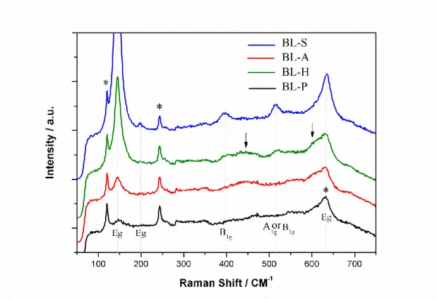
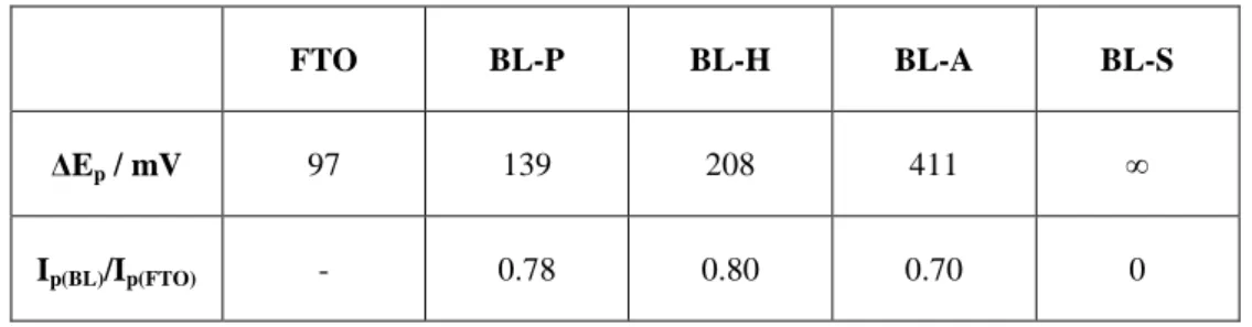
Dans le Chapitre 2, nous avons étudié les paramètres qui rendent les couches bloquantes de TiO2 efficaces. Plusieurs BLs ont été préparées par la technique de
pyrolyse-spray et par spin-coating. Nous avons trouvé que les premières étaient minces, très compactes et parfaitement couvrantes. Par spectroscopie Raman, nous avons montré qu’elles étaient constituées d’anatase pure et la voltamétrie cyclique a montré qu’elles étaient parfaitement bloquantes. Les couches préparées par spin-coating étaient poreuses, contenaient des craquelures et des trous et n’étaient pas complètement bloquantes. De plus elles étaient moins cristallisées que celles préparées par pyrolyse spray et contenaient de la phase rutile. Nous avons aussi utilisé la spectroscopie d’impédance pour étudier les différents phénomènes de transfert et d’accumulation de charges se déroulant dans le dispositif sous éclairement et comment ils sont influencés par la BL.
Dans le chapitre 3, nous avons étudié le phénomène de cristallisation spontanée de la pérovskite FAMA (FA0.87MA0.13Pb(I0.87Br0.17)3 avec FA le cation formamidinium
et MA le action methylammonium) par le contrôle de la concentration de supersaturation de la solution de précurseur. Nous avons développé deux types de dépôts de la pérovskite, le dépôt direct et la technique de dépôt à chaud (hot-casting). La technique de dépôt direct sans étape d’induction de la cristallisation par égouttement par un anti-solvant a permis d’obtenir une phase α pure. Elle pourrait permettre l’obtention des films homogènes sur une large surface. La technique de hot-casting a permis d’obtenir des couches denses, formées de gros grains et de phase α pure. Ces couches présentaient beaucoup moins de joints de grains ce qui devrait permettre de limiter fortement leur effet néfaste de recombinaison de charges. Cependant, ces couches présentaient des crêtes qui sont à l’origine de défauts et de propriétés photovoltaïques décevantes. Nous avons enfin étudié la préparation de la pérovskite FAMA par la technique d’égouttement (dripping) d’un antisolvant pour induire la crystallisation et finalement obtenir des dispositifs PV très performants et reproductibles. L’étude de 30 cellules a donné les paramètre PV moyens suivants : Voc = 1104 mV, Jsc = 23.16 mA/cm2, et FF = 78%, soit un rendement de photoconversion
moyen (PCE) de 19.8%.
De plus, nous avons mené une étude détaillée de l’extraction de charge par les couches adjacentes en utilisant les techniques de mesure de déclin de photoluminescence (PL) (technique TCSPC) et de spectres de PL stationnaires. Nous avons montré que le temps de vie des porteurs de charges et donc le temps d’extraction dépend de la pérovskite et de la couche d’oxyde. La structure planaire TiO2-compact conduit à un trasfert d’électrons peu rapide et est donc peu efficace.
D’un autre côté, la structure TiO2-compact/mesoporeuse/PCBM est beaucoup plus
efficace et permet de générer un photocourant beaucoup plus élevé. Il existe donc une marge d’amélioration pour les dispositifs du côté de cette couche qui collecte et transporte les électrons.
Dans le chapitre 4, nous avons étudié l’ajout de 5% de cation cesium (Cs+) dans la structure pérovskite FAMA. Nous avons étudié les premières étapes de la nucléation et montré que l’ajout de Cs favorise la nucléation hétérogène. Ce changement de composition diminue l’énergie de cristallisation. La présence de Cs améliore la pureté de la pérovskite et favorise l’obtention de la phase α. Nous avons montré que cette grande pureté améliore la stabilité de la pérovskite dans le temps et en température. Nous avons proposé un mécanisme différent de photoluminescence de la pérovskite en presence de Cs. De plus, nous avons aussi testé cette pérovskite à triple cation monovalent avec la couche d’extraction électronique TiO2-compact/mesoporeuse/PCBM. Avec cette configuration, les cellules ont atteint
un Jsc très élevé de 24.61 mA/cm2
Finalement, nous avons obtenu des dispositifs de rendement tr s éè levé , s reproductible et stable avec la pérovskite Cs5FAMA. Pour les cellules record, nous avons mesuré : Voc = 1104 mV, Jsc =24.19 mA/cm2, et FF = 77.4%, soit un PCE de 20.67 %. Le suivi sur 5 minute de la puissance maximale élivrées d adonnéun rendement stable de 20.6%. Les paramètres photovoltaïques moyens mesurés pour 40 cellules étaient de Voc = 1106 mV, Jsc = 23.84 mA/cm2, FF = 76%, donnant un PCE de 20.2 %.
Abstract
In sun, hydrogen and helium be lighted to generate atomic nuclei combine and release heavier energy by fusion reaction. Human beings never give up grabbing renewable energy from sun. Photovoltaic devices always deem the best candidate for a renewable energy.
Since the 50’s, photovoltaics is a field in continuous development, from the earlier developed crystalline silicon to thin film solar cells, and then to the more recent dye-sensitized solar cells (DSSCs) and organic solar cells. Recently, a new family of very promising solar cells, derived from DSSCs, appeared based on new absorber materials, the hybrid perovskites (HPs). In perovskite solar cells (PSCs), organic and inorganic hybrid perovskites with a general formula ABX3replaces the pigment in
DSSCs, and exhibits an extremely high optical absorption coefficient and a tunable band gap via composition change. Meanwhile, to improve the device stability, traditional liquid electrolyte is replaced by a solid state hole transporting materials (HTM). Based on these advanced improvements, the power conversion efficiency (PCE) of PSC has rapid increased from 3.8% to certified 22.7% within a few years. In this thesis, we have optimized the TiO2 hole blocking layer (BL) and we have
investigated multiple monovalent cation (A in ABX3) perovskite compounds for PSC
application. Finally we realized a series of stable, reproducible and highly efficient PSCs.
Chapter 1 is a bibliographic review of solar cells and PSC components as well as a description of the main techniques employed for the device characterizations. In the chapter 2, we have investigated the key parameters that render the TiO2 BL efficient in
PSCs. Several BLs have been prepared using the aerosol spray pyrolysis and the spin-coating techniques. We found that the sprayed BLs present thin, highly compact, full-covering characters. They exhibited the pure anatase phase characters by Raman spectroscopy, and realized perfectly blocking effect via cyclic voltammetry. On the other hand, the spin-coated layers were porous, contained cracks and pinholes and were not fully blocking. They were less crystallized than the sprayed layers. Besides,
we developed the use of the impedance spectroscopy technique to investigate the various processes taking place in the cells under illumination and how they are influenced by the BL.
In the chapter 3, we have investigated the promotion of spontaneous crystallization and growth of FAMA (FA0.87MA0.13Pb(I0.87Br0.17)3 with FA the formamidinium cation
and MA the methylammonium one) perovskite by the control the supersaturation concentration of the precursor solution. We developed two kinds of perovskite deposited techniques, the simply direct film-forming and the hot-casting method. The direct film-forming without dripping process realized high purity perovskite α-phase and could be used for deposition at the large scale. The hot-casting technology realized a dense, big-grain, and pure phase perovskite layer, in order to further decrease grain boundaries and eliminate its detrimental effect on the charge carriers recombinations. Due to the morphological ridge structures of the hot-casted perovskite, these layers did not demonstrate excellent photovoltaic properties. Then we adopted an anti-solvent dripping step to trigger crystallization and finally realized high efficiency and highly reproducible perovskite photovoltaic devices. The investigation of 30 FAMA photovoltaic devices exhibited the following average photovoltaic parameters; Voc = 1104 mV, Jsc = 23.16 mA/cm2, and FF = 78%, from which it resulted an average power conversion efficiency (PCE) of 19.8%.
In addition, we have carried out a detailed investigation of the charge extraction for the various layers by time-resolved photoluminescence (TCSPC technique) and steady-state photoluminescence (PL) spectroscopy. We obtained reasonable conclusions about the effect of the perovskite composition on the charge carrier injection kinetics and separation. We explained that the planar structure of TiO2-compact ETL usually not attain excellent photovoltaic properties due to slow
charges injection. We found that the TiO2-compact/mesoporous/PCBM ETL achieved
much more efficient electron injection. Then we concluded that the finding of a new electron transport material that could improve electron injection could breakthrough a new solar cells record.
cation (Cs+) into the dual cation FAMA perovskite. Our analysis of the early stage nucleation kinetics before heating treatment has shown that the addition of Cs promotes the heterogeneous nucleation compared to FAMA. It indicated that the crystallization Gibbs free energy of the system was decreased. The XRD patterns comparison between Cs5FAMA and FAMA perovskite showed that the Cs cation introduction into the perovskite matrix reduces the possibility of phase segregation and promotes the purity of the photoactive black α-phase. The higher phase purity further prevents perovskite phase decomposition under the high temperature operational conditions. It is a key element to make sure that solar cells can operate in a stable manner. Based on energy band theory, we propose a photoluminescence mechanism for Cs5FAMA and predict that Cs5FAMA belongs to direct semiconductors. In addition, we designed a new electron extraction layer of TiO2-compact/mesoporous/PCBM, this configuration cells achieved a very high Jsc of 24.61 mA/cm2.
Finally, we achieved high efficiency, reproducible, and stable devices with Cs5FAMA perovskite. These photovoltaic devices exhibited at best an open circuit voltage Voc = 1104 mV, a short circuit current Jsc =24.19 mA/cm2, and a fill factor FF = 77.4%, resulting in a PCE of 20.67 %. The maximum power point tracking for 5 minutes of the cells produced a steady-state PCE of 20.6%. The average photovoltaic parameters were Voc = 1106 mV, Jsc = 23.84 mA/cm2, FF = 76%, and PCE of 20.2 % for 40 piece of independent devices.
I
Contents
General introduction ... 1 Chapter 1 Context ... 3 1.1 Introduction ... 3 1.1.1 Solar energy ... 31.1.2 Standard solar spectral irradiance ... 4
1.2 Several kinds of photovoltaic solar cells ... 5
1.2.1 Silicon solar cells ... 6
1.2.2 Dye-sensitized solar cells ... 9
1.3 Perovskite solar cells ... 11
1.3.1 Developing of Perovskite solar cells ... 11
1.3.2 The perovskite component ... 13
1.3.3 Structure of perovskite solar cells ... 15
1.3.3.1 The electron transport layer ... 16
1.3.3.2 The perovskite layer ... 16
1.3.3.3 The hole transporting layer ... 18
1.3.3.4 The back contract electrode ... 20
1.4 Characterization and analysis of Perovskite solar cells ... 20
1.4.1 Solar cell’s characterization ... 20
1.4.2 Materials characterization in PSC ... 22
References ... 23
Chapter 2. TiO2 electron transport layer (ETL) Optimization and achievement of high efficiency MAPI perovskite solar cells by two-step deposition method. ... 32
2.1 Introduction ... 32
2.2 Experiments ... 33
2.3 Results and discussion ... 34
2.4 Conclusion ... 52
References ... 55 Chapter 3. Formamidinium and methylammonium dual organic cations hybrid
II
perovskite solar cells ... 61
3.1 Introduction ... 61
3.2 Experiments ... 62
3.3 Results and discussion ... 66
3.3.1 Preparation of high purity FAMA perovskite by direct film-forming method ... 66
3.3.2 Big-sized grains of FAMA perovskite prepared by hot-casting method ... 72
3.3.3 High efficiency FAMA perovskite by anti-solution method. ... 76
3.4 Conclusion ... 87
References ... 89
Chapter 4 Multiple cations lead trihalide perovskite for solar cells with higher stability, reproducibility and highest efficiency. ... 91
4.1 Introduction ... 91
4.2 Experiments ... 92
4.3 Results and discussion ... 94
4.3.1 The nucleation kinetics of perovskite ... 95
4.3.2 Nature of fluorescence mechanism in Cs5FAMA perovskite ... 96
4.3.3 Discussion on the phase changes in perovskite ... 99
4.3.4 Discussion on the perovskite thermo-stability ... 102
4.3.5 The charge carriers lifetimes ... 105
4.3.6 Design and discussion of the charge extraction layers ... 106
4.3.7 The properties of Cs5FAMA perovskite solar cells ... 110
4.4 Conclusion ... 118
References ... 120
General conclusion and perspectives ... 123
List of figures ... 126
List of tables ... 132
1
General introduction
The sun is a huge ball of very hot gas, mostly composed of hydrogen and helium, which supplies a huge, continuous, renewable and cheap energy to the earth. Human beings never give up grabbing renewable energy from sun. In photovoltaic devices, this energy can be converted into electricity that can be conveniently employed and stored.
Since the 50’s, photovoltaics is a field in continuous development, from the first developed crystalline silicon to thin film solar cells, and then to the more recent dye-sensitized solar cells (DSSCs) and organic solar cells. Recently, a new family of very promising solar cells, derived from DSSCs, appeared based on new absorber materials, the hybrid (organic and inorganic) perovskites (HPs). In perovskite solar cells (PSCs), compounds with a general formula ABX3 replaces the pigment in DSSCs,
and exhibits an extremely high optical absorption coefficient and a tunable bandgap via composition change. Meanwhile, to improve the device stability, traditional liquid electrolyte is replaced by a solid-state hole transporting material (HTM). Based on these advanced improvements, the power conversion efficiency (PCE) of PSCs has steadily and rapidly increased from 3.8% to certified 22.7% within a few years. In this thesis, we have optimized the TiO2 hole blocking layer (BL) and we have
investigated multiple monovalent cation (A in ABX3) perovskite compounds for PSC
application. Finally we realized a series of stable, reproducible and highly efficient PSCs.
Chapter 1 is a bibliographic review of solar cells and PSC components, as well as a description of the main techniques employed for the device characterizations. In addition, we further introduce perovskite solar cells development and revolution in the past few years, including the progress achieved in the various functional layers, cells structure, and some other hot-point studies of PSCs.
2
blocking layer (BL) efficient in PSCs. Several BLs have been prepared using the aerosol spray pyrolysis and the spin-coating techniques. Besides, we develop the use of the impedance spectroscopy technique to investigate the various processes taking place in the cells under illumination and how they are influenced by the BL. The optimal TiO2 blocking layer was employed to get relatively high efficiency
CH3NH3PbI3 photovoltaic devices.
In Chapter 3 we will develop two kinds of perovskite deposition techniques avoiding a dripping step: the simple direct film-forming and the hot-casting methods. The direct film-forming without dripping process could be used for deposition at the large scale. The hot-casting technology realized a dense, big-grain, and pure phase perovskite layer. In this Chapter 3 we investigate the promotion of spontaneous crystallization and growth of FAMA (FA0.83MA0.17Pb(I0.83Br0.17)3 (with FA the
formamidinium cation and MA the methylammonium one) perovskite by the control the supersaturation concentration of the precursor solution. In the last section, we will adopt an anti-solvent dripping step to trigger crystallization and finally realize high efficiency perovskite photovoltaic devices.
In Chapter 4, the effect of adding 5% of Cs cation into the dual cations FAMA perovskite will be studied. We will analyze the early period nucleation kinetic of these materials before heating treatment, and discuss mixed-phases (other non-photoactive phases) that affect both FAMA and Cs5FAMA perovskite solar cells. Undesired mixed-phases in the FAMA perovskite will be identified. We will study the photoluminescence mechanism in FAMA and Cs5FAMA and study the charge injection to the adjacent charge collecting layers. Based on these fundamental data, high efficiency, reproducible, and stable devices with Cs5FAMA perovskite will be prepared.
3
Chapter 1 Context
1.1 Introduction
1.1.1 Solar energy
The sun is a huge ball of very hot gas, mostly composed of hydrogen and helium. The two light hydrogen nuclei combine to produce a fusion reaction which releases a helium nuclei and energy due to a slight mass loss. “A tiny loss of mass produces a huge liberation of energy” making our earth so wonderful and unbelievable. Without the sun, there would be no life on earth. We depend on the sun for obtaining energy all the time.
The traditional source of energy is coming from fossil fuels. At the same time, a mass combustion brings the terrible environmental damages, the particles matter (PM 2.5) increasing in air[1] and global warming caused by the continuous increasing of CO2 in
the atmosphere.[2] In addition the globe energy crisis problem is coming, lacking of fossil fuel will be more and more prominent as time goes on.[3]
Therefore, the sustainable and renewable energies such as wind, photovoltaics, hydropower and others will play an increasing role in the future. The report
‘Renewable Energy Capacity Statistics 2015’ released by the International Renewable Energy Agency, provides the most comprehensive, up-to-date information on renewable energy capacity around the world (see Figure 1.1).[4] It presents trends in the development of the renewable energy sector, noting that over 100 GW of new renewable power capacity has been added every year since 2011.
4
Figure 1.1 Renewable power capacity and cumulative capacity, from the report Renewable Energy Capacity Statistics 2015 by International Renewable Energy Agency (IRENA).
1.1.2 Standard solar spectral irradiance
The actual solar spectrum received by a photovoltaic device will vary due to the weather, season, time of day and location. Therefore, the standard spectra are defined to allow the performance comparison of photovoltaic devices from different manufactures and research laboratories.
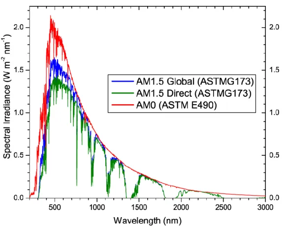
The spectra are standardized by the American Society of Testing and Materials Group (ASTMG). Figure 1.2 provides three main standardized spectra.[5] The standard spectrum for space applications is referred to as Air Mass zero (AM0), based on ASTM standard E 490. It has an integrated power of 1366.1 W/m2. Due to the absorption and scattering when sunlight passes through the atmosphere, the solar spectral irradiance is decreased. Two standards are defined for terrestrial use, based on ASTM standard G173-03. The AM1.5 Global spectrum is designed for flat plate modules and has an integrated power of 1000 W/m2 (100 mW/cm2). The AM1.5 Direct (circumsolar) spectrum is defined for solar concentrator work. It includes the direct beam from the sun plus the circumsolar component in a 2.5 degrees disk around the sun. The direct plus circumsolar spectrum has an integrated power density of 900 W/m2.
5
Since perovskite photovoltaic devices aim at being used on earth and without concentration, the cells prepared during this thesis were measured under standard AM1.5 G solar illumination.
Figure 1.2 Reference solar irradiation spectra according to the standards by the American Society of Testing and Materials.
1.2 Several kinds of photovoltaic solar cells
Photovoltaic solar cells are harvest sunlight devices which can absorb sunlight energy and convert it to electrical energy. Generally speaking, sunlight excites charge carriers or excitons in the corresponding absorber materials, the charge carriers are then separated to achieve the accumulation of electrons on one side and holes on the other side, then the charges are separated to produce a current.
Depending on the absorber materials, photovoltaic solar cells are divided into various technologies such as silicon solar cells [6, 7], dye-sensitized solar cells[8, 9], organic solar cells (such as polymer solar cells)[10, 11]. The perovskite solar cells, based on hybrid perovskite absorber materials, are newcomers and the most advanced
6
promising technology.[12] In the following, we will introduce several main families of photovoltaic devices.
1.2.1 Silicon solar cells
The first generation of photovoltaic solar cells is mainly based on crystalline silicon solar cells. It represents the main photovoltaic products on the commercial market at present (more than 90% of the market share).[13] However, the growth of crystalline silicon requires a high temperature melting which increases their fabrication cost and requires high energy consumption.[14] Therefore silicon solar cells have long period of cost recovery time. Fortunately, the silicon photovoltaic material is very stable and can be productive for several decades lasting periods.
Silicon solar cells are based on a p-n homojunction which produces a built-in electric field. It is noteworthy that the p-n homojunction is a characteristic for silicon solar cells, which is different to the dye-sensitizer solar and perovskite solar cells discussed in the following.
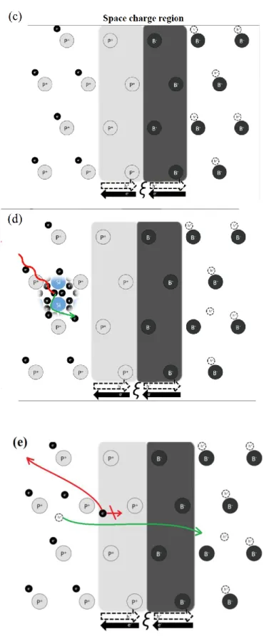
The understanding of the charge carrier separation and functioning mechanism is very necessary. The silicon absorber can be produced as two types of semiconductor materials, p-type and n-type, depending on doping. When the silicon lattices are doped by boron (or by another element of the group III column of the periodic table), this element traps the free electrons and release free holes leading to an excess of mobile holes. The semiconductor is then p-type doped. Similarly when silicon lattices are doped by phosphorus (or another element of the group V column), valence electrons have the tendency to be release and the concentration of mobile electrons increases, the semiconductor (SC) is n-type (see Figure 1.3a). All the excess charges are free to move around randomly. When two types semiconductors are contacted each other, a p-n junction is formed. Due to the opposite charges attract each other, excess electrons in the n-type will flow into the p-type to recombine with excess holes, resulting in the electron-hole neutralize and effectively vanish. Similarly, holes also can flow toward the n-type semiconductor (Figure 1.3b). Consequently, electrons and
7
holes randomly defuse and neutralize continuously at the p-n junction. The total number of mobile charges decreases continuously near the p-n junction. It results in a strong built-in electric field (i.e. a space charge region (SCR) where the charges are exhausted) and the charges diffusion process will be stopped (Figure 1.3c). Under sunlight irradiation, electron of silicon is excited near the SCR, produces a hole and starts to move randomly (Figure 1.3d). Due to the presence a strong built electric field in the SCR, the electron will only randomly diffuse in the n-type zone while the hole will drift in the SCR (Figure 3e). Finally, the charge carriers separation is realized. In the closed circuit, the electrons will travel through the external wire and finally reach the p-type zone where they will combine with holes and finally generate a continuous current in the external circuit.
8
Figure 1. 3 Silicon solar cells operating mechanism. (a) Silicon materials doping to form p-type and n-type semiconductor. (b) p-n junction formation. (c) Formation of the built-in electric field. (d) A pair of electron-hole formation after sunlight irradiation. (e) Realized charge carriers separation and current generation.
9
1.2.2 Dye-sensitized solar cells
Dye-sensitized solar cells (DSSCs) are photoelectrochemical cells that have gained a widespread attention because of low-cost production.[15] It is based on a junction formed between a photo-sensitized anode and an electrolyte forming a photoelectrochemical system. The first low cost, high-efficiency dye-sensitized solar cell was reported in 1991 by M. Grätzel’s group.[16] At present, the highest efficiency lies around 13% (11.9% for a certified cell). It has been achieved by using a porphyrin-sensitizer and a liquid electrolyte.[17] Although the liquid electrolyte presents a serious challenge for making DSSCs useable for very long time without degradation, this technology presents a good performance/price ratio that could allow DSSCs to compete with crystalline silicon solar cells by grid parity.[18]
Generally speaking, a typical Dye-sensitized solar cell includes a titanium dioxide nanoparticles photo-anode sensitized to solar light by a dye, an opposite electrode and an electrolyte containing a redox couple system and additives.[19, 20] The specific DSSC photovoltaic device architecture is shown in Figure 1.4.[21]
10
In here, with the help of Figure 1.5, we explain the DSSCs operation mechanism in detail. It will help following discussions on perovskite solar cells [22] because the first perovskite solar cells were derived from traditional DSSCs.
Charge carriers generation processes: At the beginning, the incident photons are absorbed by the dye-sensitizers anchored onto TiO2 nanoparticle film. Generally, a
Ru-complex photosensitizer (N719) is used as the dye. [23, 24] The photosensitizers are excited under sunlight, the electrons are excited form the ground state (S) to the excited state (S∗). At the same time, the electric charge is transferred to the TiO2 wide
bandgap oxide and it results in the oxidation of the photosensitizer (S+).
S S*
S S+ +
e
-Electrons diffusion processes: The electrons, injected into the conduction band of TiO2, are transported by diffusion between the TiO2 nanoparticles toward the
transparent conducting oxide (TCO) front contact. Finally, the electrons reach the counter-electrode (CE) through the external circuit.
Electrolyte redox reaction: The oxidized photosensitizer (S+) accepts electron from the I− ion redox mediator leading to regeneration of the ground state (S), and two I− ions are oxidized to elementary iodine which reacts with I− to the oxidized state I3−.
S+ +
e
- SThe oxidized redox mediator, I3− diffuses toward the counter electrode and then it is
reduced to I− ions. I3
―
+2
e
- 3I―It is noteworthy that just electrons are transported by diffusion mechanisms in dye-sensitized solar cell. The photogenerated electrons pass through the external circuit and flow into electrolyte where the redox reaction occurs.
11
Figure 1. 5 Dye-sensitized solar cell device working mechanism.[22]
1.3 Perovskite solar cells
1.3.1 Developing of Perovskite solar cells
As discussed above, silicon solar cell has a p-n junction to form a built-in electric field. This electric potential field allows an effective separation of electrons and holes. In the DSSCs, a liquid electrolyte is used as a redox system. However, this electrolyte can be replaced by a solid hole transporting material (HTM), and covered a top metal counter electrode to constitute a solid-state dye-sensitized solar cells (ssDSSCs). In addition, the dye-sensitizer (such as the N719 dye and other pigments) can be replaced by a new inorganic and organic hybrid lead trihalide material (i.e. perovskite) to constitute a new family of solar cells. These photovoltaic devices are called perovskite solar cells (PSCs). Therefore the perovskite solar cells are derived from the DSSCs. However, further studies showed that the mesoporous TiO2 has to be quite
thin (several hundred nm) and the perovskite layer had to be quite thick (several hundred nanometers) for getting record efficiencies. Moreover, earlier studies showed that the mesoporous TiO2 layer could be replaced by a mesoporous layer made of
insulating ZrO2. It has been also shown that planar architectures, without mesoporous
TiO2 layer can work very effectively, just by using a compact thin TiO2 layer, or better,
12
The perovskite solar cells have attracted a widespread attention in recently years. The power conversion efficiency of these devices has followed an unprecedented rapid rise from 3.8% to 22.7% within a few years. Figure 1.6 shows the evolution of the certified record for single junction perovskite solar cells which achieved a 22.7% efficiency in 2017. The rapid development of perovskite solar cells promote to form a independent solar cell branch―perovskite solar cell. The correlative mechanism, theory, and a series of new materials are developing, and the perovskite solar cell is the most cutting-edge research in photovoltaic field, which enforced power conversion efficiency (PCE) rapidly increasing just in the past several years (see Figure 1.7).
Figure 1.6 Chart of perovskite solar cell efficiency records by the National Renewable Energy Laboratory (NREL).[25]
13
Figure 1.7 Performance evolution chart of the best certified research cell efficiencies as published by NREL.[25]
1.3.2 The perovskite component
Historically, the term perovskite was used to describe the materials with the same type of crystal structure as calcium titanium oxide (CaTiO3), which was discovered in 1839
by the mineralogist Gustav Rose (named perovskite in honor of the Russian mineralogist Lev Alexeïevitch Perovski).[26] However, the discovery of organometal halide perovskite, mixing both organic and inorganic components by D. Weber is much more recent (1978).[27, 28] Their chemistry and descriptions have been then developed by several groups, in particular by D.B. Mitzi and co-workers.[29, 30] Depending on their structure, one can distinguish the 3D and 2D halide perovskite compounds. Most of them are direct bandgap semiconductors with a high light absorption coefficient.
The 3-dimensions organic-inorganic hybrid perovskite material has an ABX3 structure,
where A is typically an organic cation (methylammonium, MA+; formamidinium, FA+) but can also be the cesium cation (Cs+). A is 12-fold cuboctahedral coordinated to X anions. B is a divalent metal cation B (Pb2+, Sn2+, Ge2+), and X is an anion (Cl-, Br-, I-).
14
The ideal cubic-symmetry perovskite structure has the B cation in 6 fold coordination, surrounded by the BX6 octahedron anions, and BX6 octahedron are corner-connected
to form a three dimensional framework (see Figure 1.8). Due to the presence of a rather big space in the center of the cubic perovskite structure, small organic cations can fill the formed cage. The most miraculous is that, when the various A cations are adopted, it can distort the perovskite crystal structure and further induces many physical and chemistry properties. Especially, the electronic, magnetic, ferrimagnetism, and ferroelectric properties of the material [31] depend on the details of these distortions, which are important for the application of perovskite material.[32, 33]
In the photovoltaic field, organic-inorganic hybrid perovskite is easy to synthesize at low temperature by processes using solutions. Perovskite have strong panchromatic absorption of sunlight especially in the visible-light wavelength. In addition, perovskite are direct semiconductors with a tunable energy bandgap between 1.2 eV to 2.2 eV by adjusted chemical compositions engineering. Low exciton binding energy is approximate10 meV and long charge carrier diffusion length is around 1 μm, especially in single crystals, which is guaranteed that charge carries can be effective separated. And their charges mobilities are roughly 10 cm2·v-1·s-1. These unique photophysical and optoelectronic properties explain why perovskite solar cells achieved very high power conversion efficiency, low-costing and convenient fabrication.
15
1.3.3 Structure of perovskite solar cells
If the initial structure of the PSC was based on DSSCs (using a liquid electrolyte and perovskite nanocrystals for sensitization), the major breakthroughs in the field were realized in 2012 when a solid HTM (typically Spiro-OMeTAD) was employed to replace the liquid electrolyte (in which the perovskite is dissolved, making the devices unstable) and with the use of rather thick perovskite layers of typically 400 nm thickness.[35] With the development of perovskite solar cells (PSCs), the device structure and configuration also presents a series of evolution and change. For example, the inverted structure PSCs [36, 37, 38], planar PSCs [39, 40], and mesoscopic PSCs [12, 41, 42] have been developed in parallel. In the inverted structure devices, the hole extracting layer is deposited on ITO substrate, the electron extraction layer is prepared on top of the perovskite layer and the back contact is deposited on this layer. It is completely the opposite to the ‘normal’ or standard PSCs structure. Very recently, an inverted structure device has been reported to achieve an efficiency above 20%.[43]
In here, we mainly introduce the ‘normal’ or standard perovskite solar cell structure. As shown in Figure 1.9, these PSCs consist in an electron transporting layer (including a compact hole blocking and a mesoporous layer), a perovskite layer, a hole transporting layer, and a metal back-contact electrode. The energy levels matching for the various functional layers will decide the device structure and the final efficiency.
16
Figure 1.9 Standard structure of perovskite solar cells and functional layer assemblies (the left schematic). Cross section SEM image of a standard perovskite solar cells (right image). The insets are pictures of FAMA and Cs5FAMA –based perovskite solar cells.
1.3.3.1 The electron transport layer
In order to prevent charge carriers recombination on transparent conducting oxide (TCO), one must first avoid the direct contact between the F-doped tin oxide (FTO) and the perovskite. Therefore, a dense metal oxide hole blocking layer is deposited that must completely covers the FTO surface. In addition, through the energy levels matching between the compact metal oxide and the perovskite, promoted electrons must be rapidly injected into the metal oxide conduction band from perovskite. Generally speaking, the electron transporting layer (ETL) of high efficiency PSCs consists in a bilayer structure: a compact layer capped by a mesoporous layer (see Figure 1.9). In the chapter 3 and 4, we will show that, in the case of TiO2, a double
layer ETL can extract more efficiently the photogenerated electrons.
Several techniques have been developed to fabricate the metal oxide ETL. Aerosol spray pyrolysis and spin-coating are the most commonly techniques used.[35][44] The typical thickness of a blocking layer ranges between 20 and 100 nm, which can be controlled by the concentration of the precursor solution and the spin-coating time.[45] The mesoporous TiO2 layers are prepared from a nanoparticle solution at the accurate
concentration, spin-coated on top of the hole blocking layer. In the Chapter 2, we will detail various techniques and precursor solutions for the preparation of the TiO2 hole
blocking layer in PSCs and their effect on the cell performances and functioning.
1.3.3.2 The perovskite layer
Absorber materials for the solar light harvesting must have a broad and strong absorbance over the visible to near infrared region of the solar spectrum. Shockley
17
Queisser efficiency limit theory gives maximum efficiency at the band gap of 1.34 eV.[46]
These bandgap values determine the strength of electrical field which is related to the open circuit voltage of the solar cell. When the bandgap value is too low, a wider solar spectrum will be covered and this absorber material will collect extra current by absorbing more photons. However, it also results in a smaller voltage. On the other hand, a larger bandgap value will generate a lower current (due to a narrower absorption wavelength range for light) and a higher voltage. In this case, to balancing these two effects, the optimal band gap for a single junction solar cell is between about 1.4-1.5 eV.[47]
The organic-inorganic hybrid perovskites have attracted a widespread attention, because their optical bandgap can be varied by changing the A cation, the metal cation and/or the halide anion.
The bandgap of traditional perovskites such as CH3NH3PbI3 and CH3NH3PbI3-xClx
usually used in the literature, is 1.58 eV[47, 48] and 1.55 eV[49], respectively. Later, some research groups found that pure formanidinium (FAPbI3) perovskite also
achieved 14.2% efficiency for a bandgap of 1.48 eV.[47] In addition, one cation that has recently attracted much attention in mixed cation perovskite is the inorganic cesium (Cs+) which ionic radius is 1.81 Å [50, 51]. It is considerably smaller than MA+ (2.70 Å) or FA+ (2.79 Å).[52] In the FA0.9Cs0.1PbI3 perovskite, FA+ is partially
replaced by Cs+, the device PCE was enhanced to 16.5%.[53] Michael Saliba et al. found that the completely inorganic of CsPbI3 perovskite can be crystallized at high
temperature and with a bandgap at around 1.73 eV.[54] Finally the α-CsPbI3 (PSCs)
displayed an highly reproducible efficiency of 11.8%.[55]
Concerning the influence of the metal cation, taking the example of AMI3 (M=Sn, Pb),
the band gap of ASnI3 (1.20 eV) is lower than that of APbI3 (1.58 eV).[56]
Researchers have investigated the influence of the halide anion, the mixed-halide (I1-xBrx) composition also adjusted perovskite bandgap value from 1.48 to 2.3 eV in
FAPb(I1-xBrx).[57]
18
sufficient to induce a preferable crystallization into the photoactive phase of FA perovskite resulting in a more thermally and structurally stable composition than the pure MA or FA compounds.[58, 59] This illustrates that MA can be thought as a “crystallizer” of the black phase FA perovskite.[50, 60, 61, 62] We found the MA/FA mixed perovskite is a research hot spot, because it presents excellent properties and PCE record.[54, 59, 60, 61]
Many deposition techniques of perovskite layers have been developed in the literature. The common film deposition methods are so called one-step precursor solution depositions [63] and the two-step sequential deposition method.[44] Besides, several groups have developed the vacuum-assisted method[64], the hot-casting method [37] and the anti-solvent methods [65, 66]. It is noteworthy that anti-solvent dripping treatment is successfully used to trigger perovskite crystallization. S. Paek et al. studied the effect of various anti-solvents on perovskite crystallization.[67] The dual-source vapor deposition method permits to prepare an extremely uniform perovskite layer. An efficiency of 15.4% was reported by Liu et al.[68] Y. Yang’s group reported a low-temperature vapor-assisted solution process to get perovskite film with full surface coverage, and finally achieved a PCE of 12.1%.[40] Michael Grätzel’s group adopted a vacuum flash-assisted solution process for the perovskite layer preparation and attained high certified PCE of 19.6%.[69]
1.3.3.3 The hole transporting layer
The hole transporting layer (HTL) is another key components in perovskite solar cells. It is used to extract holes and inject holes into the back contact in PSCs. Various materials have been explored as HTM, ranging from low HOMO molecular[70], polymers[71, 72] and inorganic component such as CuI [73] or CuSCN[74]. In a typical perovskite solar cell, the most commonly used hole transporting material (HTM) is 2,2’,7,7’-tetrakis-N,N-di(4-methoxyphenyl)amine-9,9’-spirobifluorene (noted Spiro-OMeTAD). The molecular structure of Spiro-OMeTAD is depicted in Figure 1.10. Spiro-OMeTAD is an amorphous organic p-type semiconductor with a
19
large bandgap (at about 3.0 eV). This compound has a hole mobility in the range of 1 10-5 to 1 10-4 cm2 V-1 s-1 as reported in the literature.[75, 76] The advantage of spiro-OMeTAD is its good ability to pore filling due to the high solubility in toluene and chlorobenzene organic solvents.
Figure 1. 10 Molecular structure of
2,2’,7,7’-tetrakis-N,N-di(4-methoxyphenyl)amine-9,9’-spirobifluorene (Spiro-MeOTAD), utilized as HTM in PSCs.
Pristine spiro-OMeTAD has high resistivity. Therefore, non-doped Spiro-OMeTAD HTM usually cannot achieve high efficiency. Generally speaking, several additives are added to Spiro-OMeTAD solution to improve its rapid holes transporting properties. The common additives are: 4-tert-butylpyridine (TBP), lithium bis(trifluoromethylsulfonyl)imide (LiTFSI) attributed, and tris(2−1H-pyrazol-1-yl)-4-tert-butylpyridine)-cobalt(III)-tris(bis-(trifluoromethylsulfo nyl)imide) (a cobalt complex which directly oxidizes the Spiro-OMeTAD). However, these additives into HTM bring some problems to PSCs. Especially, the 4-tert-butylpyridine (TBP) and Li complex chemicals could react with the counter electrode.[77, 78] In addition, some researchers think that the Spiro-OMeTAD dopants can diffuse into the metal electrode causing irreversible degradation.[79, 80] Therefore, some researchers turn to studying new HTM materials. For example, Yi Hou et al. reported that using Ta-WOx/conjugated polymer PDCBT in the hole
20
extraction layer realizes high efficiency and stable working PSCs.[81] Besides, Neha Arora et al. reported that using configuration of CuSCN/graphene oxide HTL allows the achievement of high efficiency, around 20%, and that the PSCs retain > 95% of their initial efficiency after a 1000 hour of functioning.[82] It is observed that Spiro-OMeTAD maybe not the best candidate for HTM in PSCs.
1.3.3.4 The back contract electrode
The back contact electrode of PSCs usually use silver or gold thin film formed by the thermal evaporation technique. Silver is more used than gold, due to a lower cost. However, the gold back electrode can supply a suitable work function, which promotes the achievement of a high voltage for photovoltaic devices. Compared to the expensive silver and gold contacts, the low-cost carbon materials have attracted some attention especially with the layer preparation by screen printable deposition techniques.[41] Moreover, the carbon layer can work as a water repellent layer to protect the cell from water, and improves the stability of PSCs devices.[83] [84]
1.4 Characterization and analysis of Perovskite solar cells
1.4.1 Solar cell’s characterization
Current-Voltage (J-V curves) characteristics
The solar cells were measured under a one sun illumination provided by a solar simulator (Abet Technology Sun 2000) using a 150 W xenon light source. The light intensity was calibrated with a Si photodiode. Current-voltage characteristics of the cells were obtained by applying an external voltage bias while measuring the current response with a digital sourcemeter (Keithley 2410). The voltage scan rate was 25 mV s-1 and no device preconditioning, such as light soaking or extended forward voltage biasing in the dark, was applied before starting the measurement. The cells were masked with metal mask (0.076 cm2) to fix the active area and reduce the influence of the scattered light. The metal mask was calibrated by using an optical microscope
21
which has permitted to precisely measure the mask active area at 0.076 cm2. The incident light intensity was adjusted to 1000 W/m2 in accordance with standard AM 1.5G specrum (see Figure 1.2) by using a calibrated silicon solar cell.
Stabilized power output and stability measurements
Steady-state power output and stability of solar cells were performed with a Princeton Applied Research (EGG 273A model) potentiostat under the same solar simulator with standard AM 1.5G illumination.The devices were masked (0.076 cm2) under the normal ambient atmosphere. After the opening of the shutter of the solar simulator, the devices were measured with a maximum power point (MPP) tracking routine, under the monitored potentiostat. 30 tracking points were recorded in 60 s. For stabilized power output experiments, the measurement time was 60 s. For photovoltaic devices stability experiments, the measurement time was 300 s.
External quantum efficiency (EQE)
In order to determine the ratio of collected charge to the incident photons, the external quantum efficiency was introduced. The devices were measured with a QuantX-300 apparatus from Newport Corporation equipped with a monochromator and a 150 W xenon lamp. The light beam was chopped at 25 Hz and the wavelength measurement ranged from 300 nm to 900 nm.
Impedance spectroscopy
The impedance spectra were measured at room temperature, between 600 kHz and 30 mHz, using a PGSTAT 30 apparatus from Autolab. All the measured cells had the same contact geometries. The alternating current (AC) signal was 20 mV. All the impedance spectra were measured at room temperature, over a large potential range (typically from 0V to 1V), both in the dark and under a ~1 sun light power provided by a halogen Schott lamp. These spectra were analyzed using the Z-view software from National Instrument.
22
1.4.2 Materials characterization in PSC
X-ray power diffraction
The various pristine perovskite films were measured by an X’Pert Pro diffractometer (Malvern Pananalytical) equipped with ceramic copper anode tube (CuKα, λ = 1.5406
Å). Diffraction patterns were collected for 15 min.The measurements were performed in Bragg-Brentano geometry 2θ =8° to 80°.
Field emission scanning electron microscope (FE-SEM)
Scanning electron microscopy (SEM) was performed on a high-resolution scanning electron microscope (ZEISS Merlin). Secondary electron images were acquired with an EDX detector. Reflecting back scatting electron images were obtained with RBSE detector by split screen technology.
Steady-state photoluminescence spectrum measurements
Photoluminescence spectra were recorded by exciting the perovskite films deposited on various extraction layers at 460 nm with a standard 450-W Xenon CW lamp. The signal was obtained on a spectrofluorometer (Fluorolog FL1065, Horiba Jobin Yvon Technology) in the 620 nm to 850 nm range. The samples were mounted at 60° and the emission recorded at 90° from the incident beam path.
Time-resolved photoluminescence decay spectrum measurements (with single-photon counting, TCSPC technique)
The PL decay experiments were performed under microscope observation (numerical aperture 0.7). The sample was excited by a 470 nm diode laser (Picoquant). The emission was filtered by a 488-nm longpass filter. The emission signal was analyzed by a PerkinElmer SPCM avalanche photodiode combined with a Picoharp acquisition card (500 ps characteristic time of the total system response function) used with the laser in a pulsed mode at a 0.14 µW excitation power (pulse duration 70 ps).
23
Steady-state absorbance spectrum measurements (with time increasing absorbance dynamic spectrum)
The absorption spectra (specular component) of the various layers were measured by a Varian Cary 5000 UV-Vis-NIR spectrophotometer.
For the study of perovskite nucleation kinetics in Chapter 4, the mesoporous TiO2
layer were deposited on FTO glasses and infiltrated with perovskite precursor solution by spin-coating. Immediately, the sample was mounted into a special sample holder, and then the anti-solvent was rapidly injected on perovskite precursor film. The film optical absorption was then monitored at 495 ~ 500 nm wavelengths, and absorbance points were recorded by every single 6 second.
Optical microscopy
Electronic optical microscopy was employed to precisely measure the metal mask surface area to obtain the accurate illuminated solar cell area.
References
1. Peters A, Dockery DW, Muller JE, Mittleman MA. Increased particulate air pollution and the triggering of myocardial infarction. Circulation. 2001;103:2810-5. 2. Shakun JD, Clark PU, He F, Marcott SA, Mix AC, Liu Z, Otto-Bliesner B, Schmittner A, Bard E. Global warming preceded by increasing carbon dioxide concentrations during the last deglaciation. Nature. 2012;484:49.
3. Rubin ES, Chen C, Rao AB. Cost and performance of fossil fuel power plants with CO2 capture and storage. Energy policy. 2007;35:4444-54.
4. IRENA RELEASES WORLD’S MOST COMPREHENSIVE RENEWABLE
ENERGY CAPACITY FIGURES. Available from:
https://irenanewsroom.org/2015/06/14/irena-releases-worlds-most-comprehensive-ren ewable-energy-capacity-figures/.
5. Standard Solar Spectra. Available from: https://www.pveducation.org/pvcdrom/appendices/standard-solar-spectra.
24
6. Wenham S, Green M. Silicon solar cells. Progress in Photovoltaics: Research and Applications. 1996;4:3-33.
7. Goetzberger A, Knobloch J, Voss B. Crystalline silicon solar cells. editorial John Wiley & Sons Ltd. 1998;1.
8. Grätzel M. Dye-sensitized solar cells. Journal of Photochemistry and Photobiology C: Photochemistry Reviews. 2003;4:145-53.
9. Hara K, Arakawa H. Dye‐sensitized solar cells. Handbook of photovoltaic science and engineering. 2003:663-700.
10. Wöhrle D, Meissner D. Organic solar cells. Advanced Materials. 1991;3:129-38. 11. Günes S, Neugebauer H, Sariciftci NS. Conjugated polymer-based organic solar cells. Chemical reviews. 2007;107:1324-38.
12. Grätzel M. The light and shade of perovskite solar cells. Nature materials. 2014;13:838.
13. Green MA. Commercial progress and challenges for photovoltaics. Nat Energy. 2016;1:15015.
14. Tairov YM, Tsvetkov V. Investigation of growth processes of ingots of silicon carbide single crystals. Journal of crystal growth. 1978;43:209-12.
15. Green MA. Third generation photovoltaics: advanced solar energy conversion. Physics Today. 2004;57:71-2.
16. O'regan B, Grätzel M. A low-cost, high-efficiency solar cell based on dye-sensitized colloidal TiO2 films. Nature. 1991;353:737.
17. Mathew S, Yella A, Gao P, Humphry-Baker R, Curchod BF, Ashari-Astani N, Tavernelli I, Rothlisberger U, Nazeeruddin MK, Grätzel M. Dye-sensitized solar cells with 13% efficiency achieved through the molecular engineering of porphyrin sensitizers. Nature chemistry. 2014;6:242.
18. Eshetu GG, Armand M, Ohno H, Scrosati B, Passerini S. Ionic liquids as tailored media for the synthesis and processing of energy conversion materials. Energy & Environmental Science. 2016;9:49-61.
19. Gong J, Liang J, Sumathy K. Review on dye-sensitized solar cells (DSSCs): fundamental concepts and novel materials. Renewable and Sustainable Energy
25 Reviews. 2012;16:5848-60.
20. Hamann TW. The end of iodide? Cobalt complex redox shuttles in DSSCs. Dalton Transactions. 2012;41:3111-5.
21. Tanaka exclusively supply ruthenium dye for dye-sensitized solar cell. Available from:
https://www.printedelectronicsworld.com/articles/4062/tanaka-exclusively-supply-rut henium-dye-for-dye-sensitized-solar-cells.
22. Yun S, Freitas JN, Nogueira AF, Wang Y, Ahmad S, Wang Z-S. Dye-sensitized solar cells employing polymers. Progress in Polymer Science. 2016;59:1-40.
23. Wang Z-S, Kawauchi H, Kashima T, Arakawa H. Significant influence of TiO2 photoelectrode morphology on the energy conversion efficiency of N719 dye-sensitized solar cell. Coordination chemistry reviews. 2004;248:1381-9.
24. Lee KE, Gomez MA, Elouatik S, Demopoulos GP. Further understanding of the adsorption mechanism of N719 sensitizer on anatase TiO2 films for DSSC applications using vibrational spectroscopy and confocal Raman imaging. Langmuir. 2010;26:9575-83.
25. NREL chart (2018) https://www.nrel.gov/pv/assets/images/efficiency-chart.png. 26. Mitzi DB. Templating and structural engineering in organic–inorganic perovskites. Journal of the Chemical Society, Dalton Transactions. 2001:1-12.
27. der Verbindungen TIS. CH3NH3PbX3, ein Pb (II)-System mit kubischer Perowskitstruktur.
28. Weber D. CH3NH3SnBrxI3-x (x= 0-3), ein Sn (II)-System mit kubischer Perowskitstruktur/CH3NH3SnBrxI3-x (x= 0-3), a Sn (II)-system with cubic perovskite structure. Zeitschrift für Naturforschung B. 1978;33:862-5.
29. Mitzi D, Wang S, Feild C, Chess C, Guloy A. Conducting layered organic-inorganic halides containing< 110>-oriented perovskite sheets. Science. 1995;267:1473-6.
30. Kagan C, Mitzi D, Dimitrakopoulos C. Organic-inorganic hybrid materials as semiconducting channels in thin-film field-effect transistors. Science. 1999;286:945-7.
26
31. Frost JM, Butler KT, Walsh A. Molecular ferroelectric contributions to anomalous hysteresis in hybrid perovskite solar cells. Apl Materials. 2014;2:081506.
32. Feng HL, Arai M, Matsushita Y, Tsujimoto Y, Guo Y, Sathish CI, Wang X, Yuan Y-H, Tanaka M, Yamaura K. High-temperature ferrimagnetism driven by lattice distortion in double perovskite Ca2FeOsO6. Journal of the American Chemical Society. 2014;136:3326-9.
33. Aso R, Kan D, Shimakawa Y, Kurata H. Atomic level observation of octahedral distortions at the perovskite oxide heterointerface. Scientific reports. 2013;3:2214. 34. Green MA, Ho-Baillie A, Snaith HJ. The emergence of perovskite solar cells. Nature Photonics. 2014;8:nphoton. 2014.134.
35. Kim H-S, Lee C-R, Im J-H, Lee K-B, Moehl T, Marchioro A, Moon S-J, Humphry-Baker R, Yum J-H, Moser JE. Lead iodide perovskite sensitized all-solid-state submicron thin film mesoscopic solar cell with efficiency exceeding 9%. Scientific reports. 2012;2:591.
36. He Z, Zhong C, Su S, Xu M, Wu H, Cao Y. Enhanced power-conversion efficiency in polymer solar cells using an inverted device structure. Nature Photonics. 2012;6:591.
37. Nie W, Tsai H, Asadpour R, Blancon J-C, Neukirch AJ, Gupta G, Crochet JJ, Chhowalla M, Tretiak S, Alam MA. High-efficiency solution-processed perovskite solar cells with millimeter-scale grains. Science. 2015;347:522-5.
38. Bai Y, Yu H, Zhu Z, Jiang K, Zhang T, Zhao N, Yang S, Yan H. High performance inverted structure perovskite solar cells based on a PCBM: polystyrene blend electron transport layer. Journal of Materials Chemistry A. 2015;3:9098-102.
39. Liu D, Kelly TL. Perovskite solar cells with a planar heterojunction structure prepared using room-temperature solution processing techniques. Nature Photonics. 2014;8:133.
40. Chen Q, Zhou H, Hong Z, Luo S, Duan H-S, Wang H-H, Liu Y, Li G, Yang Y. Planar heterojunction perovskite solar cells via vapor-assisted solution process. Journal of the American Chemical Society. 2013;136:622-5.
27
hole-conductor–free, fully printable mesoscopic perovskite solar cell with high stability. Science. 2014;345:295-8.
42. Park N-G. Organometal perovskite light absorbers toward a 20% efficiency low-cost solid-state mesoscopic solar cell. The journal of physical chemistry letters. 2013;4:2423-9.
43. Luo D, Yang W, Wang Z, Sadhanala A, Hu Q, Su R, Shivanna R, Trindade GF, Watts JF, Xu Z. Enhanced photovoltage for inverted planar heterojunction perovskite solar cells. Science. 2018;360:1442-6.
44. Burschka J, Pellet N, Moon S-J, Humphry-Baker R, Gao P, Nazeeruddin MK, Grätzel M. Sequential deposition as a route to high-performance perovskite-sensitized solar cells. Nature. 2013;499:316.
45. Wang P, Shao Z, Ulfa M, Pauporté T. Insights into the hole blocking layer effect on the perovskite solar cell performance and impedance response. The Journal of Physical Chemistry C. 2017;121:9131-41.
46. Shockley W, Queisser HJ. Detailed balance limit of efficiency of p‐n junction solar cells. Journal of Applied Physics. 1961;32:510-9.
47. Eperon GE, Stranks SD, Menelaou C, Johnston MB, Herz LM, Snaith HJ. Formamidinium lead trihalide: a broadly tunable perovskite for efficient planar heterojunction solar cells. Energy & Environmental Science. 2014;7:982-8.
48. Etgar L, ao P, Xue , Peng , Chandiran A , Liu B, Nazeeruddin M , r tzel M. Mesoscopic CH3NH3PbI3/TiO2 heterojunction solar cells. Journal of the American Chemical Society. 2012;134:17396-9.
49. Lee MM, Teuscher J, Miyasaka T, Murakami TN, Snaith HJ. Efficient hybrid solar cells based on meso-superstructured organometal halide perovskites. Science. 2012:1228604.
50. Yi C, Luo J, Meloni S, Boziki A, Ashari-Astani N, Grätzel C, Zakeeruddin SM, Röthlisberger U, Grätzel M. Entropic stabilization of mixed A-cation ABX 3 metal halide perovskites for high performance perovskite solar cells. Energy & Environmental Science. 2016;9:656-62.
28
Harlang T, Chabera P, Pullerits T, Stepanov A. Organometal halide perovskite solar cell materials rationalized: ultrafast charge generation, high and microsecond-long balanced mobilities, and slow recombination. Journal of the American Chemical Society. 2014;136:5189-92.
52. Amat A, Mosconi E, Ronca E, uarti C, mari P, Nazeeruddin M , r tzel M, De Angelis F. Cation-induced band-gap tuning in organohalide perovskites: interplay of spin–orbit coupling and octahedra tilting. Nano letters. 2014;14:3608-16.
53. Lee JW, Kim DH, Kim HS, Seo SW, Cho SM, Park NG. Formamidinium and cesium hybridization for photo‐and moisture‐stable perovskite solar cell. Advanced Energy Materials. 2015;5:1501310.
54. Saliba M, Matsui T, Domanski K, Seo J-Y, Ummadisingu A, Zakeeruddin SM, Correa-Baena J-P, Tress WR, Abate A, Hagfeldt A. Incorporation of rubidium cations into perovskite solar cells improves photovoltaic performance. Science. 2016;354:206-9.
55. Zhang T, Dar MI, Li G, Xu F, Guo N, Grätzel M, Zhao Y. Bication lead iodide 2D perovskite component to stabilize inorganic α-CsPbI3 perovskite phase for high-efficiency solar cells. Science advances. 2017;3:e1700841.
56. Stoumpos CC, Malliakas CD, Kanatzidis MG. Semiconducting tin and lead iodide perovskites with organic cations: phase transitions, high mobilities, and near-infrared photoluminescent properties. Inorganic chemistry. 2013;52:9019-38. 57. McMeekin DP, Sadoughi G, Rehman W, Eperon GE, Saliba M, Hörantner MT, Haghighirad A, Sakai N, Korte L, Rech B. A mixed-cation lead mixed-halide perovskite absorber for tandem solar cells. Science. 2016;351:151-5.
58. Bi D, Yi C, Luo J, Décoppet J-D, Zhang F, Zakeeruddin SM, Li X, Hagfeldt A, Grätzel M. Polymer-templated nucleation and crystal growth of perovskite films for solar cells with efficiency greater than 21%. Nature Energy. 2016;1:16142.
59. Bi D, Tress W, Dar MI, Gao P, Luo J, Renevier C, Schenk K, Abate A, Giordano F, Baena J-PC. Efficient luminescent solar cells based on tailored mixed-cation perovskites. Science advances. 2016;2:e1501170.
![Figure 1. 4 Device architecture of a typical liquid dye-sensitized solar cell.[21]](https://thumb-eu.123doks.com/thumbv2/123doknet/2720609.64435/20.892.162.728.685.1074/figure-device-architecture-typical-liquid-sensitized-solar-cell.webp)
![Figure 1.6 Chart of perovskite solar cell efficiency records by the National Renewable Energy Laboratory (NREL).[25]](https://thumb-eu.123doks.com/thumbv2/123doknet/2720609.64435/23.892.254.618.459.942/figure-perovskite-efficiency-records-national-renewable-energy-laboratory.webp)
![Figure 1.7 Performance evolution chart of the best certified research cell efficiencies as published by NREL.[25]](https://thumb-eu.123doks.com/thumbv2/123doknet/2720609.64435/24.892.137.784.123.479/figure-performance-evolution-chart-certified-research-efficiencies-published.webp)
![Figure 1. 8 Ball and stick model of generic ABX 3 perovskite structure.[34]](https://thumb-eu.123doks.com/thumbv2/123doknet/2720609.64435/25.892.269.631.852.1114/figure-ball-stick-model-generic-abx-perovskite-structure.webp)