HAL Id: tel-01935468
https://tel.archives-ouvertes.fr/tel-01935468
Submitted on 26 Nov 2018
HAL is a multi-disciplinary open access
archive for the deposit and dissemination of
sci-entific research documents, whether they are
pub-lished or not. The documents may come from
teaching and research institutions in France or
abroad, or from public or private research centers.
L’archive ouverte pluridisciplinaire HAL, est
destinée au dépôt et à la diffusion de documents
scientifiques de niveau recherche, publiés ou non,
émanant des établissements d’enseignement et de
recherche français ou étrangers, des laboratoires
publics ou privés.
Locally Synchronous), Non-Volatile Integrated Circuit
for Space Applications
Jeremy Lopes
To cite this version:
Jeremy Lopes. Design of an Innovative GALS (Globally Asynchronous Locally Synchronous),
Non-Volatile Integrated Circuit for Space Applications. Micro and nanotechnologies/Microelectronics.
Université Montpellier, 2017. English. �NNT : 2017MONTS052�. �tel-01935468�
Préparée au sein de l’école doctorale I2S
∗Et de l’unité de recherche SPINTEC
∗∗, LIRMM, CNES
Spécialité: Systèmes Automatiques et Micro-Électroniques
Présentée par Jeremy Lopes
Conception de Circuit Intégré Innovant
Asynchrone, Non-Volatile pour
Application Spatiale
Soutenue le 18/09/2017 devant le jury composé de :
Pr. Alex Yakovlev Professeur Newcastle University Rapporteur Pr. Jean-Michel Portal Professeur Aix-Marseille Université Rapporteur Pr. Laurent Dusseau Professeur Université de Montpellier Président du Jury Dr. Edith Beigné HDR CEA Examinateur Dr. David Dangla Ingénieur R&D CNES Examinateur Pr. Lionel Torres Professeur Université de Montpellier Directeur de Thèse Dr. Gregory Di Pendina IR CNRS Laboratoire Spintec Co-encadrant
• Gregory Di Pendina - For his support, time and ideas that made this doctorate productive and very stimulating, as well as his support with spintronics.
• Lionel Torres - Who made sure the doctorate was going to plan.
• The members of the jury - Pr. Laurent Dusseau for having agreed to preside this work, Pr. Alex Yakovlev and Pr. Jean-Michel Portal for having agreed to report this work. • Edith Beigné - For her support in the asynchronous domain as well as providing the integrated
test code that was adapted for use in the structure.
• David Dangla - For his support in the radiation domain as well as for the heavy ion testing. • François Duhem - For the time he spent adapting the FPGA tester to be able to drive the chip. • Eldar Zianbetov, Kotb Jabeur & Pierre Vanhauwaert - For their help with all new
pro-grammes I discovered and used during these three years, as well as for their support.
• CEA-LETI/DACLE/LISAN - For the test architecture RTL code and more particularly Jean-Frédéric Christmann, David Coriat & Sylvain Choisnet who were a huge help im-plementing and debugging the integrated test code and elements.
• Kevin Sanchez - For his help with the laser testing.
• Robin Rolland and Michele Portolan - For giving us access to the source codes for their FPGA tester.
• Guillaume Prenat - For his help setting up and helping with the different programmes used during this Ph.D.
• Rachel Mauduit and Catherine Broisin - For their help with all the administration in the CEA.
• Nicolas Serrurier and Caroline Lebrun - For their help with the administration in the LIRMM and the doctoral school inscriptions.
Summary
Today, there are several ways to develop microelectronic circuits adapted for space applications that meet the harsh constraints of immunity towards radiation, whether in terms of technical design or manu-facturing process. The aim of this doctorate is on the one hand to combine several novel techniques of microelectronics to design architectures adapted to this type of application, and on the other hand to incorporate non-volatile magnetic components inherently robust to radiation. Such an assembly would be quite innovative and would benefit without precedent, in terms of surface, consumption, robustness and cost.
In contrast with synchronous circuit designs that rely on a clock signal, asynchronous circuits have the advantage of being more or less insensitive to delay variations resulting for example from variations in the manufacturing process. Furthermore, by avoiding the use of a clock, asynchronous circuits have relatively low power consumption. Asynchronous circuits are generally designed to operate based on events determined using a specific handshake protocol. The basic circuit element of an asynchronous design is a circuit known as a C-element or Muller cell. This circuit includes a volatile latch for storing a state. Thus if the asynchronous circuit is powered down, the data stored by the various C-elements will be lost. An asynchronous pipeline is generally formed in stages, each stage comprising a half buffer formed of several C-elements.
For aviation and/or spatial applications, it would be desirable to provide an asynchronous circuit that is rendered robust against the effects of radiation. Indeed, the presence of ionising particles at high altitudes or in space can induce currents in integrated circuits that may be enough to cause a flip in the binary state held by one or more gates. This may cause the circuit to malfunction, known in the art as a single event upset (SEU). It has been proposed to provide dual modular redundancy (DMR) or triple modular redundancy (TMR) in an asynchronous circuit design in order to provide radiation protection. Such techniques rely on duplicating the circuit in the case of DMR, or triplicating the circuit in the case of TMR, and detecting a discordance between the outputs of the circuits as an indication of the occurrence of an SEU. A problem with the DMR technique is that it does not permit the error to be corrected, and thus when an error is detected, the circuit is simply reset. This adds a time delay, as the processing operation must be restarted. Furthermore, if SEUs occur at a relatively high rate, it may even be impossible for a processing operation to be completed before a reset is required. The TMR technique does allow the error to be corrected, for example by selecting the output value generated by two out of three of the circuits using a majority voter. However, a drawback with the TMR technique is that the surface area and power consumption of the circuit are increased by a factor of three.
The integration of inherently robust non-volatile components, such as Magnetic Tunnel Junctions (MTJ), the main element of MRAM memory, could lead to new ways of data retention in harsh envi-ronments. MTJ devices are constituted of ferromagnetic materials with magnetic properties that are not sensitive to radiation. Data is stored in the form of the direction of the magnetisation and not in the form of an electric charge, which is an essential property for space applications. It is also widely recognised in the field of microelectronics that integrated circuits manufactured on SOI (Silicon On Insu-lator) substrates are more robust to radiation. This is due to the reduced active volume of the individual transistors as well as their isolation in regards to each other. The radiation-induced errors are very localized and therefore cannot be spread from one block to another, thanks to the insulation provided by the manufacturing process. Another important characteristic of SOI is its natural immunity towards latch-ups.
There is thus a need in the art for a circuit having relatively low surface area and power consumption, and that allows recovery following an SEU without requiring a reset and that has non-volatile characteris-tics. The objective of this doctorate is to combine all the above mentioned benefits by regrouping several methods of microelectronic design responding to the constraints of space applications into a novel archi-tecture. A complete circuit has been created, designed, simulated, validated and sent to manufacturing in a 28nm FD-SOI process. This circuit is composed of an adder pipeline and a complex BIST (Build In Self Test). When fabricated, this circuit will be tested. First a functional test will be realised, then laser pules attacks will be performed and finally a heavy ions attack campaign.
Résumé
Aujourd’hui, il existe plusieurs façons de développer des circuits microélectroniques adaptés aux appli-cations spatiales qui répondent aux contraintes sévères de l’immunité contre les radiations, que ce soit en termes de technique de conception ou de processus de fabrication. Le but de ce doctorat est d’une part de combiner plusieurs techniques nouvelles de microélectronique pour concevoir des architectures adaptées à ce type d’application et d’autre part, d’incorporer des composants magnétiques non-volatiles intrinsèquement robustes aux rayonnements. Un tel couplage serait tout à fait novateur et profiterait sans précédent, en termes de surface, de consommation, de robustesse et de coût. Contrairement à la concep-tion de circuits synchrones qui reposent sur un signal d’horloge, les circuits asynchrones ont l’avantage d’être plus ou moins insensibles aux variations temporel résultant par exemple des variations du processus de fabrication. En outre, en évitant l’utilisation d’une horloge, les circuits asynchrones ont une consom-mation d’énergie relativement faible. Les circuits asynchrones sont généralement conçus pour fonctionner en fonction des événements déterminés grâce à un protocole de "poignée de main" spécifique. L’élément de base d’un circuit asynchrone est un bloc connu sous le nom de C-element ou de cellule de Muller. Ce circuit comprend un latch volatile pour le stockage d’un état. Ainsi, si le circuit asynchrone est éteint, les données stockées par les différentes cellules de Muller seront perdues. Un pipeline asynchrone est généralement formé par étapes, chaque étape comprenant une cellule de mémorisation formé de plusieurs cellules de Muller.
Pour les applications avioniques et spatiales, il serait souhaitable de fournir un circuit asynchrone rendu robuste contre les effets des radiations. En effet, la présence de particules ionisantes à haute altitude ou dans l’espace peut induire des courants perturbateurs dans des circuits intégrés qui peuvent être suffisants pour provoquer un basculement à l’état binaire maintenu par une ou plusieurs grilles. Cela peut provoquer un dysfonctionnement du circuit, connu dans l’état de l’art en tant que single event upset (SEU). Il a été proposé de fournir un module redondant double (Dual Modular Redundency : DMR) ou un module redondant triple (Tripple Modular Redundcy : TMR) dans une conception de circuit asynchrone afin de fournir une protection contre les radiations. De telles techniques s’appuient sur la duplication du circuit dans le cas de DMR, ou en triplant le circuit dans le cas de TMR, et en détectant une discordance entre les sorties des circuits comme indication de l’apparition d’une SEU. Un problème avec la technique DMR est qu’il ne permet pas de corriger l’erreur, et donc lorsqu’une erreur est détectée, le circuit est simplement réinitialisé. Cela ajoute une temporisation, car l’opération de traitement doit être redémarrée. En outre, si les SEU se produisent à un taux relativement élevé, il peut même être impossible qu’une opération de traitement soit terminée avant qu’une réinitialisation ne soit requise. La technique TMR permet-elle de corriger l’erreur, par exemple en sélectionnant la valeur de sortie générée par deux des trois blocs d’un circuit voteur majoritaire. Cependant, un inconvénient avec la technique TMR est que la surface et la consommation d’énergie du circuit sont augmentées d’un facteur trois.
L’intégration de composants non-volatils intrinsèquement robustes, tels que les jonctions de tunnel magnétique (JTM), l’élément principal de la mémoire MRAM, pourrait conduire à de nouvelles façons de retenir les données dans des environnements difficiles. Les dispositifs JTM sont constitués de matériaux ferromagnétiques avec des propriétés magnétiques qui ne sont pas sensibles aux rayonnements. Les données sont stockées sous la forme de la direction de l’aimantation et non sous la forme d’une charge électrique, qui est une propriété essentielle pour les applications spatiales. Il est également largement reconnu dans le domaine de la microélectronique que les circuits intégrés fabriqués sur les substrats SOI (Silicon On Insulator) sont plus robustes aux radiations. Ceci est dû à la réduction du volume actif des transistors individuels ainsi qu’à une isolation à l’égard de l’autre. Les erreurs induites par rayonnement sont très localisées et ne peuvent donc pas être réparties d’un bloc à l’autre grâce à l’isolation fournie par le procédé de fabrication. Une autre caractéristique importante du SOI est son immunité naturelle vis-à-vis des courts-circuits du type thyristor, connu sous le nom de latch up.
Il existe donc un besoin dans l’état de l’art pour un circuit ayant une surface et une consommation d’énergie relativement faibles, et qui permet une récupération après un SEU sans nécessiter de réinitia-lisation et qui présente des caractéristiques non-volatiles. L’objectif de ce doctorat est de combiner tous les avantages mentionnés ci-dessus en regroupant plusieurs méthodes de conception microélectronique répondant aux contraintes des applications spatiales dans une nouvelle architecture. Un Circuit complet a été imaginé, conçu, simulé et envoyé en fabrication. Ce circuit est composé d’un pipeline asynchrone d’additionneur et d’un test intégré complexe connu sous le nom de BIST (Built In Self Test). Apres fabrication, ce circuit sera testé. Premièrement des tests fonctionnels vont être réalisés, puis des tests sous laser pulsé seront menés ainsi que sous attaques aux ions lourds.
I
Introduction
15
II
State of the Art
19
1 MRAM Memory and Emerging Non-Volatile Memory 21
1.1 Introduction . . . 23
1.2 Spintronics . . . 23
1.3 Magnetoresistance Effect . . . 24
1.3.1 Giant Magnetoresistance . . . 24
1.3.2 Tunnel Magnetoresistance . . . 24
1.4 Magnetic Random Access Memory . . . 25
1.4.1 Reading in MRAMs . . . 25
1.4.2 Field Induced Magnetic Switching (FIMS) . . . 25
1.4.3 Field Induced Magnetic Switching: Toggle Switching . . . 26
1.4.4 Thermally Assisted Switching (TAS) . . . 27
1.4.5 Spin Transfer Torque Switching (STT) . . . 28
1.4.6 Spin Orbit Torque Switching (SOT) . . . 30
1.4.7 Comparing STT and SOT Performance . . . 31
1.5 Other Emerging Non-Volatile Memories . . . 33
1.5.1 Phase Change RAM (PCRAM) . . . 34
1.5.2 Conductive Bridging RAM (CBRAM) . . . 34
1.5.3 Resistive RAM (ReRAM) . . . 34
1.5.4 Quantitative Comparison of Emerging Memories . . . 35
1.5.5 Radiation Tolerant Emerging Non-Volatile Memory’s . . . 35
2 Asynchronous Logic 37 2.1 Introduction . . . 39
2.2 What is Asynchronous Logic? . . . 39
2.3 Asynchronous Operator Characteristics . . . 39
2.4 How Asynchronous Logic Works . . . 39
2.5 Communication Protocol . . . 39
2.5.1 2 Phase Protocol / Half-Handshake . . . 40
2.5.2 4 Phase Protocol / Full-Handshake . . . 40
2.6 Data Coding . . . 41
2.6.1 Dual Rail Coding . . . 41
2.6.2 Bundled Data Coding . . . 41
2.7 Advantages of Asynchronous Circuits . . . 42
2.8 Asynchronous Characteristics . . . 42
2.8.1 Asynchronous Hazards . . . 43
2.8.2 Different Delay Models . . . 43
2.8.3 Different Asynchronous Circuit Classes . . . 43
2.9 Globally Asynchronous, Locally Synchronous (GALS) Architecture . . . 44
2.10 Simulations . . . 45
2.10.1 Muller Gate . . . 45
3 Radiation in Space 47
3.1 Introduction . . . 49
3.2 Space Environment and Radiation Sources . . . 49
3.2.1 Different Sources of Radiation in Space . . . 49
3.2.2 The Ejection of Matter from the Sun . . . 49
3.2.3 Solar Wind . . . 50
3.2.4 Cosmic Radiation . . . 50
3.2.5 Van Allen Radiation Belts . . . 50
3.2.6 Atmospheric Neutrons . . . 51
3.2.7 Different Energies Involved . . . 51
3.2.8 Particle Concentration . . . 51
3.3 The Different Interactions . . . 52
3.3.1 Interaction with Photons . . . 52
3.3.2 Interaction with Neutrons . . . 52
3.3.3 Interaction with Charged Particles . . . 53
3.3.4 Interaction with Protons . . . 53
3.4 The Effect of Radiation on Electronic Circuits . . . 53
3.4.1 Terminology . . . 53
3.4.2 Different Types of Radiation Effects . . . 53
3.5 Means of Prevention and Protection Against SEEs . . . 55
3.5.1 Shielding . . . 55
3.5.2 Hardening of Components . . . 55
3.5.3 System Level Hardening . . . 55
3.6 Strategies for Testing Integrated Circuits . . . 56
3.6.1 Error Injection (During Design Stage) . . . 56
3.6.2 Testing in an Artificial Environment . . . 56
3.6.3 Testing in a Real Environment . . . 56
4 Silicon On Insulator Technology 57 4.1 Introduction . . . 59
4.2 Silicon On Insulator (SOI) . . . 59
4.3 Advantages of Silicon On Insulator . . . 60
III
Innovative Error Correcting 28nm FD-SOI Circuit
61
1 Preliminary Study 63 1.1 Introduction . . . 651.2 Particle Injection . . . 65
1.3 Simulation Protocol . . . 66
1.4 Radiation Induced Errors Impact on 28nm FDSOI . . . 66
1.4.1 Influence of the Supply Voltage . . . 67
1.4.2 Impact of the Threshold Voltage . . . 67
1.4.3 Influence of Body Biasing . . . 67
1.5 The Effect of Non-Volatility Towards Robustness in a Simple Structure . . . 67
1.5.1 Non-Volatile Flip-Flop . . . 67
1.5.2 Non-volatile Half-Buffer . . . 68
1.5.3 Simulation Results . . . 68
1.5.4 Results and Interpretation . . . 69
1.6 Conclusion . . . 70
2 Innovative Error Correcting Structure: Functional Mechanisms 71 2.1 Introduction . . . 73
2.2 An Error Correcting Asynchronous Structure . . . 73
2.3 A Non-Volatile Error Correcting Asynchronous Structure . . . 74
2.4 Advantages/Disadvantages of the Proposed Structure . . . 74
3 Innovative Error Correcting Structure: Design and Test 77
3.1 Introduction . . . 79
3.2 Asynchronous Communication . . . 79
3.3 Comparator . . . 80
3.4 Acknowledgement Pause . . . 81
3.5 Simulating Particle Strikes on the Volatile Version of the Proposed Structure . . . 82
3.5.1 Erroneous Result from the Adder . . . 82
3.5.2 Error on the Acknowledgement Signal . . . 83
3.5.3 Error on the Comparators Output . . . 83
3.5.4 Multiple Error Correction . . . 83
3.5.5 Limits of Correction . . . 83 3.5.6 False Errors . . . 84 3.6 Non-Volatile Section . . . 84 3.6.1 Non-Volatile Cell . . . 84 3.6.2 Pause Cell . . . 87 3.6.3 Multiplexor Cell . . . 88
3.7 Simulating Particle Strikes on the Non-Volatile version of the Proposed Structure . . . 88
3.7.1 Erroneous Result from the Adder . . . 88
3.7.2 Error on the Acknowledgement Signal or Comparators Output . . . 89
3.7.3 Error in the Pause Cell . . . 89
3.7.4 Error in Multiplexor Cell . . . 89
3.7.5 Error in the Non-Volatile Cell . . . 89
3.7.6 Multiple Error Correction . . . 90
3.7.7 Limits of Correction . . . 90
3.8 A Few Extra Things . . . 90
3.9 Conclusion . . . 90
4 Integrated Test Structure 93 4.1 Introduction . . . 95
4.2 What to Measure? . . . 95
4.3 Test Circuit . . . 95
4.3.1 Serial Peripheral Interface (SPI) . . . 96
4.3.2 Counter . . . 97
4.3.3 Frequency Locked Loop (FLL) . . . 97
4.3.4 Repeater . . . 97
4.3.5 Simulation . . . 98
4.4 Conclusion . . . 98
5 Partial Validation Through Simulations 99 5.1 Introduction . . . 101 5.2 Electric Simulations . . . 101 5.3 Digital Simulations . . . 102 5.4 Mixed Simulations . . . 102 5.5 Conclusion . . . 102 6 Physical Implementation 103 6.1 Introduction . . . 105 6.2 Layout of MTJ CELL . . . 105 6.2.1 Layout . . . 105
6.2.2 Design Rule Checking (DRC) . . . 106
6.2.3 Layout Versus Schematic (LVS) . . . 106
6.2.4 Library Exchange Format (LEF) . . . 106
6.3 Place and Route of the Whole Circuit . . . 107
6.3.1 Initialise Design . . . 107
6.3.2 Power Distribution Grid . . . 107
6.3.3 Design Placement . . . 108
6.3.4 Design Route . . . 108
6.4 Conclusion . . . 109
IV
Demonstrator and Tests
111
1 Design of the Printed Circuit Board 113 1.1 Introduction . . . 1151.2 PCB Constraints . . . 115
1.3 PCB Schematic . . . 115
1.3.1 Number of Chips on the PCB . . . 115
1.3.2 Power Adapters . . . 115
1.3.3 Single Error Output of the Laser Tests . . . 116
1.3.4 Connectors . . . 116
1.4 PCB Component Placement . . . 116
1.5 Chip Packaging . . . 117
1.6 The PCB . . . 118
2 The Different Chip Tests 119 2.1 Introduction . . . 121
2.2 Diamond D10 Circuit Tester . . . 121
2.2.1 The Tester . . . 121
2.2.2 Controlling the Tester . . . 121
2.3 The Field Programmable Gate Array (FPGA) Interface for Test . . . 122
2.3.1 FPGA Architecture . . . 123
2.3.2 Controlling the FPGA . . . 123
2.4 Pulsed Laser Test . . . 124
2.5 Heavy Ion Test . . . 124
3 Driving the Chip 125 3.1 Introduction . . . 127
3.2 The Test Programme . . . 127
3.3 The Different Programme Variations . . . 127
3.4 The Diamond D10 Circuit Tester . . . 129
3.5 The FPGA Interface for Test . . . 130
V
Conclusion and Perspectives
131
2.1.1 Spin of the Electron . . . 23
2.1.2 Magnetic Orientation in Different Materials . . . 23
2.1.3 Magnetic Tunnel Junction . . . 24
2.1.4 Reading in an MTJ . . . 25
2.1.5 Writing an MTJ with FIMS Technique . . . 26
2.1.6 Writing an MTJ with FIMS Toggle Technique . . . 26
2.1.7 Toggle Writing Sequence . . . 26
2.1.8 Writing an MTJ with TAS Technique . . . 27
2.1.9 Writing in TAS MRAM . . . 27
2.1.10 Influence of Signal Synchronisation . . . 28
2.1.11 Writing an MTJ with STT Technique: (a) Perpendicular-To-Plane, (b) In-Plane . . . . 28
2.1.12 STT Switching . . . 29
2.1.13 Reading and Writing in STT MRAM . . . 29
2.1.14 Accidental Writing while Reading in STT MRAM . . . 29
2.1.15 Writing an MTJ with SOT Technique . . . 30
2.1.16 Reading and Writing in SOT MRAM (Purple Arrows Writing and Black Arrows Reading) 30 2.1.17 Writing in SOT MRAM with no External Magnetic Field . . . 31
2.1.18 STT Non-Symmetrical Switching Current/Time . . . 32
2.1.19 SOT Symmetrical Switching Current/Time . . . 32
2.1.20 STT Switching with Different Currents . . . 32
2.1.21 SOT Switching with Different Currents . . . 32
2.1.22 The TMRs Influence on the Difference Between Two States when Reading . . . 33
2.1.23 Phase Change RAM . . . 34
2.1.24 Conductive Bridging RAM . . . 34
2.1.25 Resistive RAM . . . 34
2.2.1 Asynchronous Operators . . . 39
2.2.2 2 Phase Protocol / Half-Handshake . . . 40
2.2.3 4 Phase Protocol / Full-Handshake . . . 40
2.2.4 Dual Rail Coding: Three State Coding (left), Four State Coding (right) . . . 41
2.2.5 Asynchronous Operator Using Bundled Data . . . 41
2.2.6 Bundled Data Coding (4 Phase Protocol) . . . 42
2.2.7 Isochronic Fork . . . 43
2.2.8 Micro-pipeline Circuit Based on Muller Gates: Muller Gate Symbol (Bottom Left) and Muller Gate Truth Table (Bottom Right) . . . 44
2.2.9 GALS Asynchronous Operators . . . 44
2.3.1 Coronal Mass Ejection . . . 49
2.3.2 A Solar Flare . . . 49
2.3.3 Solar Wind . . . 50
2.3.4 Cosmic Radiation . . . 50
2.3.5 Van Allen Radiation Belts . . . 50
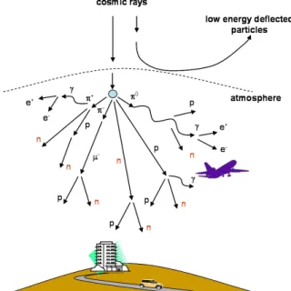
2.3.6 Atmospheric Neutrons. Where: e+ = P ositron; e− = Electron; γ = Gamma ray; π = P ion; µ = Mion; n, p = Nucleons. . . 51
2.3.7 Particle Concentration . . . 52
2.3.9 Left: Illustration of SEE, Right: Illustration of TID . . . 54
2.3.10 Triple Modular Redundancy . . . 55
2.3.11 Dual Modular Redundancy . . . 55
2.4.1 Silicon On Insulator vs. Bulk . . . 59
2.4.2 Body Biasing . . . 59
3.1.1 Examples of the Induced Current Pulses Generated by a Particle Impact, Waveforms are Simulated . . . 65
3.1.2 Examples of Transients Measured for Different Ion Strike Locations Along the Source – Drain Axis of a 0.25 µm Bulk Transistor. The Gate Length is 0.25 µm and the Transistor Width is 25 µm [32] . . . 65
3.1.3 Example of a Particle Injection (Current Pulse) in an OR Gate . . . 66
3.1.4 Graphical Representation of the Simulation Protocol . . . 66
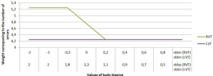
3.1.5 Graphical Representation of the Number of Particle Induced Errors Depending on the Body Biasing. . . 67
3.1.6 Dual MTJ Latch Cell (Hass): (a) STT Version, (b) SOT Version . . . 68
3.1.7 Non-Volatile C-Element: (a) STT Version, (b) SOT Version . . . 68
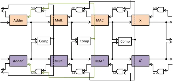
3.2.1 An Error Correcting Asynchronous Structure . . . 73
3.2.2 A Non-Volatile Error Correcting Asynchronous Structure . . . 74
3.3.1 Portion of an Asynchronous Pipeline Composed of Adders . . . 79
3.3.2 Input and Output Signals of Stage n . . . 80
3.3.3 External and Internal View of the Comparator . . . 80
3.3.4 Input and Output Signals of the Acknowledgement Pause Circuit . . . 81
3.3.5 External and Internal View of the Acknowledgement Pause Circuit . . . 81
3.3.6 Input and Output Signals of the Acknowledgement Pause Circuit . . . 81
3.3.7 Portion of the Complete Eight Stage Volatile Structure . . . 82
3.3.8 Example of Injecting an Error on a Bit of one of the Buses . . . 82
3.3.9 Timing Diagram Showing the Detection and Restoration from an Error . . . 83
3.3.10 Non-Volatile Section and its Three Sub Cells . . . 84
3.3.11 External and Internal View of the Non-Volatile Cell . . . 85
3.3.12 Reading Current Pulse: A, Amplitude after reading, B, . . . 86
3.3.13 Writing Current as a Function of Pulse Width for a 60nm MTJ . . . 86
3.3.14 Writing Current as a Function of Pulse Width for an 80nm MTJ . . . 86
3.3.15 Writing Current as a Function of Pulse Width for a 100nm MTJ . . . 86
3.3.16 External and Internal View of the Pause Cell . . . 87
3.3.17 External and Internal View of the Multiplexor Cell . . . 88
3.3.18 Timing Diagram Showing the Detection and Restoration from an Error in Non-Volatile Mode . . . 89
3.3.19 Portion of the Complete Eight Stage Non-Volatile Structure . . . 91
3.4.1 Simplified View of the Complete Circuit with SPI Internal Communication, Integrated Test Modules and Proposed Structure . . . 96
3.4.2 SPI Bus: Single Master and Multiple Slaves [83] . . . 96
3.4.3 Simplified Schematic of an FLL . . . 97
3.4.4 Register Transfer Level (RTL) Simulation of the Test Circuit . . . 98
3.5.1 Validation During the Electric Simulations . . . 101
3.5.2 Validation During the Digital Post Synthesis Simulations . . . 101
3.5.3 Validation During the Mixed Signal Simulations . . . 101
3.5.4 Simulation of an MTJ (Reg Curve: Writing Current, Green Curve: Magnetic State) . . 101
3.5.5 Simulation of the Test Circuit: Generation of the Adder Pipeline Inputs . . . 102
3.6.1 Zoom on the Reading Part of the MTJ CELLs Layout . . . 105
3.6.2 Full Layout of the MTJ CELL . . . 106
3.6.4 Zoom on the Power Distribution of the Chip . . . 107
3.6.5 Placement of the Different Cells of the Chip (Left: Simplified View, Right: View in Encounter) . . . 108
3.6.6 The Final Layout of the Circuit . . . 109
4.1.1 The Combination of the "err" Buses to Create a Single Error Signal for the Laser Tester 116 4.1.2 PCB Component Placement . . . 117
4.1.3 Left: Gaining Back side Access to the Chip, Right: Photo of a Dummy Piece of Silicon Cut to the Same Dimension as our Chip in the Packaging . . . 118
4.1.4 Photo of the Two Versions of the PCB . . . 118
4.2.1 Diamond D10 by LTX Credence . . . 121
4.2.2 Sample of Code from the Diamond D10 Circuit Tester . . . 122
4.2.3 Global Architecture of the FPGA Tester [26] . . . 123
4.2.4 Left: Illustration of SEE, Right: Illustration of a Pulsed Laser Induced SEE . . . 124
4.3.1 Simplified View of Control Programme . . . 127
4.3.2 Photo of the Diamond D10 Circuit Tester and PCB . . . 129
4.3.3 DUT Inputs Generated by the Diamond D10 Circuit Tester . . . 129
4.3.4 Photo of the FPGA Interface for Test and PCB . . . 130
2.1.1 Comparative Table of STT and SOT . . . 31
2.1.2 Evaluation of the Performance of Emerging Non-Volatile Memory Technologies (1: Poor Performance, 5: Very High Performance) [4] . . . 35
3.1.1 Comparative Table of Influence of the STT-MTJs Dimensions Towards the Number of Errors . . . 69
3.1.2 Comparative Table of Influence of the SOT-MTJs Stripe Width Towards the Number of Errors . . . 69
3.1.3 Comparative Table of Synchronous/Asynchronous, Volatile/Non-volatile and TAS/ST-T/SOT . . . 70
3.2.1 Table Showing the Differences of DMR, TMR and the Proposed Structure . . . 75
3.3.1 Table Showing the Inputs of the 16 bit Adders and their Expected Outputs . . . 79
3.3.2 Table Showing the Read Current for Different MTJ ∅ in an AP State . . . 86
3.3.3 Table Showing the Read Current for Different MTJ ∅ in a P State . . . 86
4.1.1 Table Showing the Different Specifications for the Different Tests . . . 115
Today, there are several ways to develop microelectronic circuits adapted for space applications that meet the harsh constraints of immunity towards radiation, whether in terms of technical design or manu-facturing process. The aim of this research work is on the one hand to combine several novel techniques of microelectronics to design architectures adapted to this type of application, and on the other hand to incorporate non-volatile magnetic components inherently robust to radiation. Such an assembly would be quite innovative and would benefit without precedent, in terms of surface, consumption, robustness and cost.
In contrast with synchronous circuit designs that rely on a clock signal, asynchronous circuits have the advantage of being more or less insensitive to delay variations resulting for example from variations in the manufacturing process. Furthermore, by avoiding the use of a clock, asynchronous circuits have relatively low power consumption. Asynchronous circuits are generally designed to operate based on events determined using a specific handshake protocol. The basic circuit element of an asynchronous design is a circuit known as a C-element or Muller cell. This circuit includes a volatile latch for storing a state. Thus if the asynchronous circuit is powered down, the data stored by the various C-elements will be lost. An asynchronous pipeline is generally formed in stages, each stage comprising a half buffer formed of several C-elements.
For aviation and/or spatial applications, it would be desirable to provide an asynchronous circuit that is rendered robust against the effects of radiation. Indeed, the presence of ionising particles at high altitudes or in space can induce currents in integrated circuits that may be enough to cause a flip in the binary state held by one or more gates. This may cause the circuit to malfunction, known in the state of the art as a single event upset (SEU). It has been proposed to provide dual modular redundancy (DMR) or triple modular redundancy (TMR) in an asynchronous circuit design in order to provide radiation protection. Such techniques rely on duplicating the circuit in the case of DMR, or triplicating the circuit in the case of TMR, and detecting a discordance between the outputs of the circuits as an indication of the occurrence of an SEU. A problem with the DMR technique is that it does not permit the error to be corrected, and thus when an error is detected, the circuit is simply reset. This adds a time delay, as the processing operation must be restarted. Furthermore, if SEUs occur at a relatively high rate, it may even be impossible for a processing operation to be completed before a reset is required. The TMR technique does allow the error to be corrected, for example by selecting the output value generated by two out of three of the circuits. However, a drawback with the TMR technique is that the surface area and power consumption of the circuit are increased by a factor of three.
The integration of inherently robust non-volatile components, such as Magnetic Tunnel Junctions (MTJ), the main element of MRAM memory (Magnetic Random Access Memory) could lead to new ways of data retention in harsh environments. MTJ devices, are constituted of several ferromagnetic layers separated by a thin tunnel insulator (barrier) with magnetic properties that are not sensitive to radiation. Data is stored in the form of the direction of the magnetisation and not in the form of an electric charge, which is an essential property for space applications. It is also widely recognised in the field of microelectronics that integrated circuits manufactured on SOI (Silicon On Insulator) substrates are more robust to radiation. This is due to the reduced active volume of the individual transistors as well as their isolation in regards to each other. The radiation-induced errors are very localized and therefore cannot be spread from one block to another, thanks to the insulation provided by the manufacturing process. Another important characteristics of SOI is its natural immunity towards latch-ups.
There is thus a need in the art for a circuit having relatively low surface area and power consumption, and that allows recovery following an SEU without requiring a reset and that has non-volatile charac-teristics. The objective of this doctorate was to combine all the above mentioned benefits by regrouping several methods of microelectronic design responding to the constraints of space applications into a novel architecture. After being designed and fully simulated the architecture was manufactured and tested in radiative environments.
This manuscript is divided into five chapters. Chapter 2 explores the state of the art of MRAM memory, asynchronous logic, radiation in space and Silicon on Insulator. A preliminary study of synchronous, asynchronous, MRAM-based and non-MRAM-based simple structures on a 28nm FDSOI technology node is then covered in Chapter 3. As well as the design of the proposed architecture from high level schematics representations all the way to the low level physical implementation of the chip that was produced. In Chapter 4 the design of the PCB for the previously designed chip is presented as well as the different tests and test procedures the chip will undergo. This doctoral work will then be conclude in Chapter 5. Finally Chapter 6 covers the publications and patent this work led to.
MRAM Memory and Emerging
Non-Volatile Memory
Contents
1.1 Introduction . . . 23 1.2 Spintronics . . . 23 1.3 Magnetoresistance Effect . . . 24 1.3.1 Giant Magnetoresistance . . . 24 1.3.2 Tunnel Magnetoresistance . . . 24 1.4 Magnetic Random Access Memory . . . 25 1.4.1 Reading in MRAMs . . . 25 1.4.2 Field Induced Magnetic Switching (FIMS) . . . 25 1.4.3 Field Induced Magnetic Switching: Toggle Switching . . . 26 1.4.4 Thermally Assisted Switching (TAS) . . . 27 1.4.5 Spin Transfer Torque Switching (STT) . . . 28 1.4.6 Spin Orbit Torque Switching (SOT) . . . 30 1.4.7 Comparing STT and SOT Performance . . . 31 1.5 Other Emerging Non-Volatile Memories . . . 33 1.5.1 Phase Change RAM (PCRAM) . . . 34 1.5.2 Conductive Bridging RAM (CBRAM) . . . 34 1.5.3 Resistive RAM (ReRAM) . . . 34 1.5.4 Quantitative Comparison of Emerging Memories . . . 35 1.5.5 Radiation Tolerant Emerging Non-Volatile Memory’s . . . 351.1
Introduction
An emerging non-volatile random-access memory known as Magnetic Random Access Memory (MRAM) is on its way to becoming the reference for non-volatile memory. The International Technology Roadmap for Semiconductors (ITRS) considers MRAM as one of the most promising candidates to take over the market of memory. When compared to the current market memories: Static Random Access Memory (SRAM), Dynamic Random Access Memory (DRAM) and Flash, MRAM gathers the merits of all of its competitors in overall system performance and it becomes clear that MRAM could be considered as a replacement for all these types of memory [63]. This means that in future systems there will no longer be the need for different types of memory for the cache level 1 and 2 or the storage memory [15].
MRAM being a magnetic memory, it is non-volatile and radiation immune by definition [19] since its data is not stored as an electric charge, this makes it a good candidate for military and space applications. MRAM is denser than DRAM, has faster access times for writing and reading than Flash (write: 1 to 5ns, read: 0.5 to 2ns), and has lower power consumption than SRAM (about 10 times less for STT-MTJs) [43] [76] [77]. All these characteristics give MRAM a good potential for future memory in systems and explains the high interest in research and development groups worldwide.
This chapter is organised as followed: Section 2 represents the fundamental notions of spintronics and the physics behind the magnetic tunnel junction which is the basic component of MRAM. Based on the switching mechanism, 4 types of MRAMs have been identified in literature and are presented in section 3. In section 4, a comparative study is driven to highlight the advantages of spin orbit torque magnetic tunnel junctions over spin transfer torque magnetic tunnel junctions. Finally section 5 reviews the other emerging non-volatile memory and their robustness towards radiation.
1.2
Spintronics
Spintronics is the science of placing ferromagnetic materials on the route of electrons and using their spin to influence the mobility of the electrons in the materials [50].
The spin of the electron is an intrinsic form of angular momentum. Even though it cannot be described using classical mechanics it can be assimilated to the angular momentum of a rotating mass.
The electron’s spin has two states depending on the direction of the angular momentum. If the angular momentum is clockwise then it is called "spin up", if it is counter clockwise then it is called "spin down" [64].
Figure 2.1.1: Spin of the Electron
To this rotating momentum is associated a magnetic momentum. In ferromagnetic materials Figure 2.1.2 (a) the interaction between spins tend to make them align in the same direction; this causes the magnetisation of the material. In anti-ferromagnetic materials Figure 2.1.2 (b) the interactions between spins tend to make them align but not in the same direction and this causes a global non-magnetisation of the material. Finally, in conductive materials Figure 2.1.2 (c) there are no interactions between spins, once again this causes a global non-magnetisation of the material.
1.3
Magnetoresistance Effect
When a current passes through a ferromagnetic material with a majority of "spin up" the electrons with a "spin down" are slowed, stopped or even reflected, allowing only the electrons with a "spin up" to pass through the material. This means that depending on the majority spin a ferromagnetic material can be more or less resistive.
1.3.1
Giant Magnetoresistance
The magnetoresistance effect was first used in spin valves which are based on the Giant Magnetoresistance (GMR). The GMR is a variation of the resistance on a stack of several ferromagnetic layers separated by a thin metallic layer [64].
Depending on the magnetic orientation of two ferromagnetic materials, the conductivity of the structure varies. If the two ferromagnetic materials have the same magnetic orientation (parallel), the resistance of the structure will be small because electrons can pass through the structure easily. If the two ferromagnetic materials have an opposite magnetic orientation (anti-parallel), the resistance of the structure will be large because the electrons will have more difficulty passing through the structure.
1.3.2
Tunnel Magnetoresistance
The central piece of all MRAMs today is the Magnetic Tunnel Junction (MTJ), which is based on the Tunnel Magnetoresistance (TMR). Based on the GMR principle, the MTJ is a stack of several ferromagnetic layers separated by a thin tunnel insulator (barrier). Depending on the magnetic orientation of the two layers (parallel or anti-parallel) the structure resistance changes. This is caused by the electrons being able to pass more or less easily through the device and the thin insulator. It has been proven with quantum physics that electrons can cross from one conductor to another passing through a thin insulator using the tunnel effect [73].
Figure 2.1.3 shows that the structure of the MTJ is composed of two ferromagnetic materials, one thicker than the other, separated by a thin insulator called a tunnel barrier. One of the ferromagnetic materials is thicker than the other so they are respectively called the reference layer and the storage layer.
Figure 2.1.3: Magnetic Tunnel Junction
By applying an external magnetic field that is strong enough it is possible to change the magnetic orientation of the storage layer. The magnitude of the magnetic field should be carefully chosen to have an effect on the storage layer only. In other words, the external magnetic field must not effect the magnetisation of the reference layer. Changing the magnetic orientation of the storage layer makes it possible to have the MTJ in two different states: Parallel, when both the reference and storage layers have their magnetisation in the same direction and Anti-parallel, when the reference and the storage layers have an opposite magnetic orientation. Depending in which state the MTJ is in, it has a different resistance Rp (parallel) or Rap (anti-parallel) [64].
The resistance of the MTJ can be expressed as followed. Rp is the resistance when the MTJ is in a
parallel state. θ is the angular difference between the reference and storage layer. ∆Ris the variation of
the resistance between the parallel and anti-parallel state. R(θ) = Rp+ ∆R·
(1 − cos(θ))
2 (1.1)
When in a parallel state θ = 0 ⇒ R = Rp
When in an anti-parallel state θ = 180 ⇒ R = Rp+ ∆R= Rap
T M R(%) = ∆R Rp
= Rap− Rp
Rp (1.2)
Having the biggest possible difference between Rpand Rapis very important for read sensing. Today’s
TMR start between 150% to 250% and can go up to 800% at room temperature. The bigger the TMR, the easier it will be to determine with certainty the state of the magnetic junction.
1.4
Magnetic Random Access Memory
As explained in the previous section, the central part of all MRAMs today is the Magnetic Tunnel Junction (MTJ). This junction is used to store different logic states (0 or 1) depending on the orientation of its two layers (parallel or anti-parallel).
1.4.1
Reading in MRAMs
Being able to efficiently read data stored in MRAMs is vital. As explained above MTJs have two different states, each with a different resistance. Measuring this resistance is the key to reading in MRAMs [68].
Figure 2.1.4: Reading in an MTJ
To read the data stored in an MTJ, a small current (a few µA) is injected through the junction. Depending on the value of the resistance it is possible to compare this current with a reference and determine the state of the junction. The Bigger the TMR, the easier it will be to determine the state the junction is in.
The MTJ is always read in this manner no matter which technique was used to write the data. This section covers the different writing techniques used to store information in the MTJs. It overviews the different techniques used from when MRAMs first appeared up until present day [64].
1.4.2
Field Induced Magnetic Switching (FIMS)
In the first MTJs used, two orthogonal magnetic fields were used simultaneously to change the state of the storage layer one selecting a row, the other selecting a column. This technique allowed the selection of a precise memory point in a matrix of many points. The memory point effected by the two magnetic fields would be found at the intersection of the two lines used to produce the field.
Each memory point (bit) is composed of an MTJ for storing the data, a transistor for reading the data and two lines for writing the data. The clever part of this technique is the use of two lines to produce two magnetic fields. When the MTJs are placed in a square network, one line can be used for all the MTJs in a signal column and the other can be used for all the MTJs in a signal line.
If the magnetic field produced by a signal line is not strong enough to change the magnetic orientation of the storage layer in an MTJ, the association of two magnetic fields is strong enough, and then the only bit written will be the one situated at the intersection of the two lines. All the other bits on the same line or column will not be changed because the magnetic field felt by them is not strong enough to effect their magnetisation. [64] [24]
Figure 2.1.5: Writing an MTJ with FIMS Technique
Field induced magnetic switching reaches its limit when it is miniaturised. Reducing the size of the MTJs, the transistors and the lines means that each bit is closer to its neighbours. This introduces a selectivity problem, when writing in an MTJ its neighbours are effected by the magnetic field and this could change their magnetic state thus changing their logic state.
Toggle switching was introduced by the company Everspin to eliminate the selectivity effect and is explained in the following section.
1.4.3
Field Induced Magnetic Switching: Toggle Switching
Field Induced Magnetic Toggle switching uses the same MTJ as described above but its storage layer is composed of an association of two ferromagnetic layers separated by an isolation layer called SAF (Synthetic Anti Ferromagnetic layer). These two ferromagnetic layers are coupled anti-parallel to each other due to the separation layer made out of ruthenium. This storage layer is now anti-ferromagnetic, it has a larger global magnetic force which makes it more stable to thermal fluctuations [30].
Figure 2.1.6: Writing an MTJ with FIMS Toggle Technique
To write this new MTJ, the magnetisation of the two sub-storage layers must be inverted. For this a specific sequence of magnetic fields produced by two lines are used to gradually turn the magnetic orientation by steps of 45°. This technique eliminates the selectivity problem but faces limitations when confronted with miniaturisation.
We can note that presently, Toggle MRAM is the only commercial product available worldwide.
1.4.4
Thermally Assisted Switching (TAS)
Thermally Assisted switching as its name implies also uses heat properties to switch the magnetic state of the MTJ. Current is applied through the junction which has for effect to heat it. When heated sufficiently the top AF (Anti Ferromagnetic) layers’ spins are disoriented, enabling the storage layer to be switched by applying a small magnetic field. Once switched the MTJ can be cooled by stopping the current flowing through the device, in order to let the AF layer go back to its stable state with all its spins reoriented ensuring the stability of the new state [64] [67].
Each bit is composed of an MTJ for storing the data, a transistor for reading the data and heating the junction, and only one line for writing the data.
Figure 2.1.8: Writing an MTJ with TAS Technique
This technique solves all the selectivity problems because writing in a junction involves heating it and to heat a junction it must be selected by a transistor. The TAS MRAM is less power hungry than the FIMS and the FIMS Toggle Switching MRAMs making them more suitable for large scale memory applications.
The limitations of this writing technique is its latency due to the heating/cooling time of the junction and once again scalability because of the writing field, as well as power consumption composed of heating energy and switching energy, even if this last one can be shared in the case of a memory.
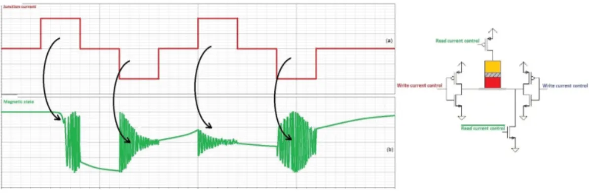
Simulations: By applying a current through the junction, the blue curve (a) in Figure 2.1.9, it is possible to heat the junction. When the junction reaches a certain temperature called the blocking temperature, which is about 150°C the magnetic orientation of the AF layer above the storage layer is disoriented. The green curve (b) in Figure 2.1.9 shows the temperature of the junction. By imposing an external magnetic field when the junction is heated enough and while it is cooling down, it is possible to change its magnetic state. In Figure 2.1.9 the red curves (c) represent the external magnetic field and the purple curves (d) represent the magnetic state of the junction.
Figure 2.1.9: Writing in TAS MRAM
The temperature of the junction is very important for the switching of magnetic states. In the left part of Figure 2.1.10, the current pulses are very short (a), this does not leave enough time for the
junction to reach the temperature where the magnetic orientation of the AF layer above the storage layer is disoriented. Thus when the external magnetic field is applied the magnetic state does not change. In the right part of Figure 2.1.10, the current pulses are very long (b) but the amount of current that passes through the junction is not sufficient to heat the junction to the point where the magnetic orientation of the AF layer above the storage layer is disoriented. Once again even with an external magnetic field, the magnetic state of the storage layer can not be changed (c) and (d).
Figure 2.1.10: Influence of Signal Synchronisation
When we look closer at the junction temperature (green curve) in Figure 2.1.9, we notice that passing from a parallel state to an anti-parallel state the temperature is lower than passing from an anti-parallel state to a parallel state. This can be explained by the difference in the resistance of the junction. When the resistance is bigger (anti-parallel) the current has more trouble passing through the junction so it does not heat up as much.
1.4.5
Spin Transfer Torque Switching (STT)
Spin Transfer Torque switching appeared with the need to reduce power consumption for MRAMs. All the previous techniques for writing data in the MTJ relied on magnetic fields, producing these magnetic fields consumed a lot of energy, even if reduced as in the case of TAS.
Figure 2.1.11: Writing an MTJ with STT Technique: (a) Perpendicular-To-Plane, (b) In-Plane STT switching uses a polarised current injected through the MTJ to switch the magnetisation of the storage layer. In an electrical current the polarisation of its spins are random. When passed through a ferromagnetic material called a polariser, the spins acquire the polarisation of the material. It is then possible for the current to transfer this polarisation to another ferromagnetic material as long as it is smaller than the polariser. The magnetisation of the FM (Ferro magnetic) layer can be either in-plane or out-of-plane, also called perpendicular-to-plane, mainly depending on its thickness. Out-of-plane requires less writing current but seems to be more difficult to control.
In such an MTJ the reference layer acts as the polariser. Depending on the direction of the current, the electrons pass the polariser or the storage layer first [27] [34] [18] [22].
Even though this technique requires a lot less current than the previous and can be miniaturised much easier, it still has a few important drawbacks. Firstly, having a common read and write path can lead to accidental writing when reading. Secondly, applying strong currents for fast writing can cause stress on the thin insulator barrier which could reduce its life span. The breakdown voltage is about 1V. Finally, non-symmetrical currents are needed to switch from one state to another. This is due to the fact that in
Figure 2.1.12: STT Switching
one case (Anti-parallel to parallel) the MTJ is written by spins going through the device and in the other case (parallel to anti-parallel) the MTJ is written by reflected spins [44] [47]. Finally, the STT-MTJ has a quasi-infinite lifespan due the deterioration caused by the writing current of the tunnel barrier. Simulations: Depending on the direction of the current injected through the junction it is possible to change the state of the magnetisation of the storage layer.
Figure 2.1.13: Reading and Writing in STT MRAM
The red curve (a) in 2.1.13 controls the positive current that changes the magnetisation from anti-parallel to anti-parallel and the blue curve (a) controls the negative current that changes the magnetisation from parallel to anti-parallel. Curve (b) Figure 2.1.13 represents the magnetic state of the storage layer. Injecting a smaller current through the junction makes it possible to read the data (logical state) in the storage layer.
The green curve (a) in Figure 2.1.13 controls the reading current applied through the junction. In part (c) of Figure 2.1.13 during two of the reading pluses, (one during the anti-parallel magnetic state and the other during the parallel magnetic state), it can be noticed that the amplitude of the red or blue curves has changed. It is with this amplitude difference that it is possible to determine in which state the magnetic junction is.
If the current injected during on the reading phase is too high, it is possible to accidentally write the junction.
In Figure 2.1.14 we can observe the accidental writing during the reading phase. The reading command signal was gradually increased then at a certain point it is visible that the magnetic state of the storage layer changes during the reading process.
1.4.6
Spin Orbit Torque Switching (SOT)
Spin Orbit Torque switching is the most recent writing technique for MRAMs and is still not fully understood. It resolves the problem of common read and write paths found in STT as both paths can be separated thanks to its three-terminal structure. A conductive line also called stripe placed under the junction is used for the writing and the reading is performed in the same manner as is STT (through the stack). However, SOT needs a slightly larger current and a small bias magnetic field to write the junction. This can either be integrated to the stack or can be external.
Writing the MTJ by SOT involves passing a current under the storage layer in a conducting line composed of a heavy metal like platinum or tantalum. This current produces a spin injection current which in turn produces a spin torque to align the magnetisation in the storage layer. Depending on the direction of the current, the magnetisation of the storage layer can be written in two different states (logical 0 or 1) under the condition of a small external magnetic field [43] [48] [56] [37].
Figure 2.1.15: Writing an MTJ with SOT Technique
SOT writing has many advantages over STT writing such as separating read and write paths and symmetrical switching currents from parallel to anti-parallel. This is due to the writing current not passing through the MTJ stack but under it. SOT is also faster than STT in terms of writing (180ps experimentally [36] [21]). Finally, since the writing current does not flow through the tunnel barrier the resistance value can be tuned by adjusting the barrier thickness. Additionally, the junction has an infinite lifespan compared to the quasi-infinite lifespan of the STT junction. SOT is still a young technique. It needs high current density for switching and its three terminal structure takes up more space than STT, so it has a lower density of high scale integration. However a lot of effort is being made at research level to optimise such devices.
Simulations: Depending on the direction of the current injected under the junction in the conductive line it is possible to change the state of the magnetisation of the storage layer.
Figure 2.1.16: Reading and Writing in SOT MRAM (Purple Arrows Writing and Black Arrows Reading) Once again the red and blue curves (a) in Figure 2.1.16 control the current that changes the magneti-sation for anti-parallel to parallel or parallel to anti-parallel. (b) in Figure 2.1.16 represents the magnetic
state of the storage layer.
Injecting a smaller current through the junction, green curve (a) in Figure 2.1.16 makes it possible to read the data (logical state) in the storage layer (c).
Figure 2.1.17: Writing in SOT MRAM with no External Magnetic Field
In part (c) of Figure 2.1.16 during two of the reading pulses, (one during the anti-parallel magnetic state and the other during the parallel magnetic state), it can be noticed again that the amplitude of the blue curve has changed. It is with this amplitude difference that it is possible to determine in which state the magnetic junction is.
Figure 2.1.17 shows a simulation where there is no external magnetic field applied. This means that the magnetic state of the MTJ cannot be written in a deterministic manner and the magnetic state visualised is nonsense.
1.4.7
Comparing STT and SOT Performance
Table 1 summarizes the main pros and cons of both STT and SOT MTJs [45] [10] [46].
STT SOT
+ Size / Density (2 terminals) - Size / Density (3 terminals) ±Writing needs high current + Low writing current density (but possibly low current if
writing strip is thin) + Low reading current + Low reading current - Common read and write paths + Separate read and write paths
- Non-symmetrical current to + Symmetrical current to switch from parallel to anti-parallel switch from parallel to anti-parallel
- Stress on the MTJ barrier + Choice of Rp/Rapvalues
during writing
- Read operation can switch - Small magnetic field is required the magnetisation state to avoid stochastic switching
- Less mature technology Table 2.1.1: Comparative Table of STT and SOT
The following simulations have the objective of confirming some of the advantages/disadvantages de-scribed in Table 2.1.1.
Symmetrical or Non-Symmetrical Switching Currents/Times
As can be seen in Figure 2.1.18 and 2.1.19, STT and SOT do not react in the same way to switching. In the following simulations, using the same current for switching from anti-parallel to parallel or parallel to anti-parallel we can observe the time it takes to switch the magnetic state.
Figure 2.1.18: STT Non-Symmetrical Switching Current/Time
Figure 2.1.19: SOT Symmetrical Switching Current/Time
SOT MTJs do not have this problem, basically because the current used to change the magnetic state passes under the junction. The resistance of the line that transports the electrons is independent to the MTJ state. Thus the electrons always see the same resistance.
Influence of the Current to Change the Magnetic State
In the following simulation we can see the influence of the amount of current used for switching magnetic states in STT and SOT MTJs.
Figure 2.1.20: STT Switching with Different Currents
By gradually decreasing the amount of current used to switch the magnetic state of the junction we can see that from a certain point the magnetic state does not change. In Figure 2.1.20 we can see that as the current decreases the junction takes more and more time to change state, and when the current is too low it does not change state (red curve).
The SOT MTJ works in the same way as the STT. When the current decreases too much the junction does not work correctly (blue curve in Figure 2.1.21) and when it is too low the junction does not switch (red curve).
In Figure 2.1.20 and 2.1.21 we can see that depending on the writing technique used (STT or SOT) different amounts of current are needed. We can see that STT needs less current than SOT to write the junction of equivalent size.
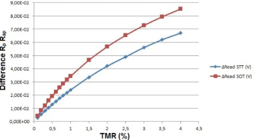
Influence of the TMR in Reading Different States
The TMR as explained earlier is the difference in resistance between the parallel and anti-parallel state. As the TMR rises, the difference between the two states becomes bigger. The bigger the difference, the easier it will be to determine the magnetic state of the MTJ with certainty.
Figure 2.1.22: The TMRs Influence on the Difference Between Two States when Reading As can be seen in Figure 2.1.22 for both STT and SOT the TMRs vary in the same manner. This is because in each technology the reading of the junction is done in the same way. We can observe that in SOT for the same TMR the difference between both states while reading is bigger, this means that it will be easier to read with certainty the state of the MTJ in SOT than in STT.
Influence of the Junction Size
For STT the size of the junction is important in terms of writing energy and resistance value to be read. For SOT the dimensions of the stripe is what matters. On one hand these sizes are limited by the technological process used to build an MTJ. The smaller the junction/stripe, the harder and more expensive it is to manufacture. On the other hand as the junction/stripe decreases in size, less current is needed to switch their magnetic state. Thus the overall consumption of the MRAM will be lower. Which Technique for MRAM Writing?
The current trends of MRAM are mainly focusing on the STT technology while keeping a dreamful eye on the SOT device as a very recent hopeful device.
Recently SOT was invented and has extremely interesting characteristics. It corrects many of the problems encountered in STT and could surpass it in the near future. SOT is a new technique and its research is not as widely spread world wide as STT but this is slowly changing.
Today it is still unclear which technique between STT and SOT will become the reference of MRAM writing, mainly due to the fact that SOT is still young. SOT is interesting due to its speed, robustness and easy integration into logic (cache L1 and L2 memory); while STT is interesting due to its density, low power consumption and easy integration into logic (mass storage, cache L2 and L3 memory).
1.5
Other Emerging Non-Volatile Memories
There are currently other types of emerging resistive memories like MRAM being developed. These mem-ories use different physical phenomenom to change the resistive properties of a combination of materials.
Thus being able to programme two distinct resistive values corresponding to the two logic values "logic high" and "logic low".
1.5.1
Phase Change RAM (PCRAM)
Phase Change RAM (PCRAM) utilises the large resistivity contrast between crystalline (low resistivity) and amorphous (high resistivity) phases of the phase change materiel. To reset the PC-RAM cell into the amorphous phase, the programming region is first melted and then quenched rapidly by applying a large current pulse for a short time period. To set the PC-RAM cell into the crystalline phase, a medium electric current pulse is applied to anneal the programming region [84].
Figure 2.1.23: Phase Change RAM
1.5.2
Conductive Bridging RAM (CBRAM)
Conductive Bridging RAM (CBRAM) is based on the polarity-dependent electrochemical deposition and removal of metal in a thin solid state electrolyte film. The ON-State is achieved by applying a positive bias larger than the threshold voltage Vthat the oxidisable anode resulting in redox reactions driving Ag
ions in the chalcogenide glass. This leads to the formation of metal rich clusters, which form a conducting bridge between both electrodes. The device can be switched off by applying an opposite voltage [53].
Figure 2.1.24: Conductive Bridging RAM
1.5.3
Resistive RAM (ReRAM)
Resistive RAM (ReRAM) also called OxRAM, is based on a conductive filament which is more or less separated from each other. By applying an electric field between the two electrodes, a conductive filament is heated by the Joule effect. This conductive filament expands, and makes the resistance vary [11].
1.5.4
Quantitative Comparison of Emerging Memories
It remains difficult to compare different families of emerging non-volatile memory technologies, the per-formances demonstrated by each of them remain under evaluation and their maturity levels are very inhomogeneous, this makes it difficult to determine representative values.
The intensification of the research effort on emerging memories has made it easier to see the potential of each technology and it is interesting to try to evaluate them. This makes it possible to evaluate the relative strengths and weaknesses of the different memory technologies. The values shown in Table 2.1.2 should be seen as an approximation of the average performance levels established for comparison between memory technologies [4].
PC- Re- CB- SOT Perp. STT Plan. STT TAS FIMS Flash RAM RAM RAM MRAM MRAM MRAM MRAM MRAM
Endurance 4 4 2 5 5 5 5 5 3 Consumption 2 3 3 3 4 4 3 2 1 Integrability 3 5 4 3 2 2 2 2 3 Scalability 4 5 5 4 4 3 3 2 1 Retention 5 4 4 3 3 3 3 3 3 Speed 4 3 3 5+ 5 5 4 5 1 Maturity 3 3 2 1 2 2 3 4 5
Table 2.1.2: Evaluation of the Performance of Emerging Non-Volatile Memory Technologies (1: Poor Performance, 5: Very High Performance) [4]
The different memories all have different and complementary advantages and all suffer from weak-nesses. This can be explained by the low levels of maturity for some of them. This comparative assess-ment confirms, that no technology has a universal character that would allow widespread use, whatever the constraints and applications. However, this technological diversification allows more flexibility by proposing different options depending on the applications targeted [4].
1.5.5
Radiation Tolerant Emerging Non-Volatile Memory’s
Out of the different emerging non-volatile memories presented in this chapter, only two are tolerant to radiation: MRAM and PCRAM [19] [53]. These two memories are immune to radiation effects because their different resistive states are programmed using magnetic orientation or phase change. As will be explained later on, radiation effects the electric charge. Since no electric charge is used to switch between resistive states in MRAM and PCRAM they can be considered immune to the effects of radiation. On the other hand, ReRAM and CBRAM both utilise the electric charge to change their resistive state, thus they could potentiality be effected by a radiative particle.
Asynchronous Logic
Contents
2.1 Introduction . . . 39 2.2 What is Asynchronous Logic? . . . 39 2.3 Asynchronous Operator Characteristics . . . 39 2.4 How Asynchronous Logic Works . . . 39 2.5 Communication Protocol . . . 39 2.5.1 2 Phase Protocol / Half-Handshake . . . 40 2.5.2 4 Phase Protocol / Full-Handshake . . . 40 2.6 Data Coding . . . 41 2.6.1 Dual Rail Coding . . . 41 2.6.2 Bundled Data Coding . . . 41 2.7 Advantages of Asynchronous Circuits . . . 42 2.8 Asynchronous Characteristics . . . 42 2.8.1 Asynchronous Hazards . . . 43 2.8.2 Different Delay Models . . . 43 2.8.3 Different Asynchronous Circuit Classes . . . 43 2.9 Globally Asynchronous, Locally Synchronous (GALS) Architecture . . . . 44 2.10 Simulations . . . 45 2.10.1 Muller Gate . . . 45 2.10.2 Half Buffers . . . 45
2.1
Introduction
The historical dominance of synchronous circuits is an undeniable fact. Nowadays the design of digital circuits borrows synchronous hypotheses almost systematically. For years, the reductive timing hypothesis has exploited the potential of the integration of technologies and the design of circuits has become increasingly complex.
Thereafter, the performance of circuits has become a strategic point. In the race to the MHz, the clock period became a much more valuable resource; today the clock is no longer an ally. In particular for the design of high-performance processors, the decrease in clock period imposes new design methodologies: Using dynamic logic, sophisticated clock trees and super-pipeline micro-architectures.
The design of most integrated logic circuits is eased by two fundamental assumptions: Binary signals are handled, and the time is discretised. Binary signals allow simple implementation and provide an electrical design framework controlled by Boolean algebra. Discretisation of time allows the overcoming of the difficulties of combinatory loops and transient power fluctuations. If asynchronous circuits retain a discrete coding for signals and are most of the time binary, they become a distinguished class for larger circuits because their control can be provided by any alternative means.
2.2
What is Asynchronous Logic?
Asynchronous means that there is no timed relation between events that are not synchronised. From an external point of view, an asynchronous operator can be considered as a cell providing a clear function and communicating with its environment through unmarked communication channels. An asynchronous logic circuit starts its operation only after the preceding operator has completed its operation.
2.3
Asynchronous Operator Characteristics
An Asynchronous operator can be characterised by at least four fundamental parameters.
• Latency: The longest time for the operator’s outputs to be a functional image of their inputs. • Cycle time: The operator’s minimum time between two accepted input data.
• Pipeline depth: The maximum amount of data the operator can memorise.
• Communication protocol: The protocol used by the operator to exchange data with its environ-ment.
2.4
How Asynchronous Logic Works
An asynchronous operator must listen to incoming communications, start its operation and produce data on its outputs when all the information needed is available on its inputs [40].
Figure 2.2.1: Asynchronous Operators
It must also be able to inform the operator before itself when it is ready to receive new data. All this is done using three signals, Acknowledgement, Data and Request. The signification of these signals will be explained in the next section.
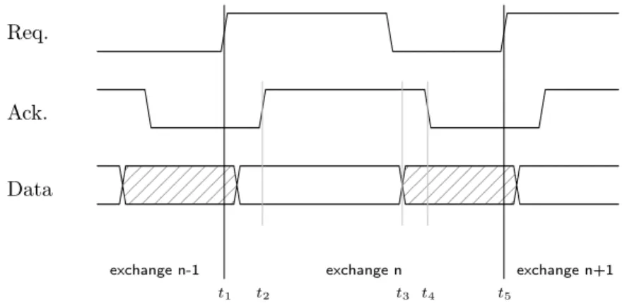
2.5
Communication Protocol
There are two main protocols used for the communication between operators: The 2 phase protocol and the 4 phase protocol. It should be noted that in both cases a change of a signal by the transmitter is