HAL Id: hal-01974805
https://hal-imt-atlantique.archives-ouvertes.fr/hal-01974805
Submitted on 9 Jan 2019HAL is a multi-disciplinary open access archive for the deposit and dissemination of sci-entific research documents, whether they are pub-lished or not. The documents may come from teaching and research institutions in France or abroad, or from public or private research centers.
L’archive ouverte pluridisciplinaire HAL, est destinée au dépôt et à la diffusion de documents scientifiques de niveau recherche, publiés ou non, émanant des établissements d’enseignement et de recherche français ou étrangers, des laboratoires publics ou privés.
Stepper based maskless microlithography using a liquid
crystal display for massively parallel direct-write of
binary and multilevel microstructures
Melanie Kessels, Marwa El Bouz, Robin Pagan, Kevin Heggarty
To cite this version:
Melanie Kessels, Marwa El Bouz, Robin Pagan, Kevin Heggarty. Stepper based maskless microlithog-raphy using a liquid crystal display for massively parallel direct-write of binary and multilevel mi-crostructures. Journal of Micro/Nanolithography, MEMS, and MOEMS, Society of Photo-optical Instrumentation Engineers, 2007, 6 (3), pp.033002. �10.1117/1.2767331�. �hal-01974805�
Stepper based maskless microlithography using a
liquid crystal display for massively parallel direct-write
of binary and multilevel microstructures
M. M. Kessels
(a), M. El Bouz
(a), R. Pagan
(b)and K. Heggarty
(a)(a) GET/ENST Bretagne
Technopˆole Brest Iroise, CS 83818, 29238 Brest Cedex 3 (France)
Phone: +33 (0)2290-01031 - Fax: +33 (0)2290-01025
(b) MIVA Technologies GmbH
Benzstr. 17, Business Park Schonaich, 71101 Schonaich (Germany)
Phone: +49 (0) 7031-75600 - Fax: +49 (0) 7031-756030
Abstract A versatile photolithographic photoplotter based on a standard photoreduction
stepper where the reticle is replaced by a commercial liquid crystal microdisplay is reported.
The microdisplay module is designed as a drop-in replacement allowing the photoplotter to
be simply and quickly converted into a standard stepper making it an extremely versatile,
low cost R&D tool. Binary and multilevel plotting are demonstrated with plot rates of
several Mpixels/s and 1 micron feature sizes into standard industrial photoresists. The
limitations on plot rate and resolution are presented and techniques for overcoming them
discussed.
Keywords lithography realtime imaging liquid crystals spatial light modulators
-micro-optics - optical fabrication
1
Introduction
In recent years, substantial research engineering effort has been directed towards
the fabrication of arbitrarily shaped 3D-microstructures because of their broad field
of applications in, for instance, the micro-optics, nanotechnology and semiconductor
industries [1–6].
These 3D-microstructures are generally fabricated either using multi-step photolithography
with standard binary masks (see for example [1]), by gray-scale photolithograhy with
coded gray-tone masks [2] or by direct-writing (laser beam [3], x-ray [4], electron beam [5]
or ion beam [6]). The first and second methods have the advantage of low cost mass
production. Mask fabrication is however a lengthy process and expensive for prototype
production. For example, the cost of a set of masks for producing a chip can exceed $
2 million [7, 8]. Moreover, in most cases, masks present little design flexibility, i.e., once
made. Direct writing, on the other hand, is a much more rapid technique for producing
small numbers of prototype 3D-microstructures: a laser spot (for example) exposes a
pattern in a thin photosensitive layer with technical simplicity and produces high quality
structures [3]. Its main disadvantage is that is unsuited to mass production because
of the tradeoff between resolution and write time: for high resolution structures the
writing-spot diameter must be small but this results in only small areas being written at
a time so the overall process is slow. Once a master structure has been made replication
techniques [9, 10] can in some cases be used to mass produce relief structures quickly and
cheaply. The prototyping remains however slow and hence expensive.
Recently new photolithographic techniques based on a real-time reconfigurable masks
have been proposed. This real-time mask is usually either a liquid crystal display (LCD)
or a digital micromirror device(DMD) used as a spatial light modulator (SLM) to control
system exposure [11–13]. The displayed images can be modified on the SLM in real
time. These techniques combine the advantages of a programmable digital LCD or
DMD system and a projection photolithography system. Conventional photolithography
is greatly simplified as a single LCD or DMD mask can replace a set of conventional
masks. For example, the alignment between different levels of masks in conventional
photolithography is no longer necessary if the LCD or DMD mask is used because the
SLM can display successively different images corresponding to different masks without
moving the substrate or the SLM, only the images displayed on the SLM change. The 3D
microstructure design can be adjusted rapidly because no mask fabrication is required,
only different data files need be generated and then displayed on the SLM.
These SLM based photoplotters present several other important advantages. First
production time is shorter than with conventional direct writing techniques for fabricating
to SLM pixels, simultaneously illuminate the photoresist, hence the term massively parallel
photoplotting. Secondly, because of this increased speed, short, custom production runs
can be performed for low cost. Finally, this technique can also constitute a powerful
tool for fabricating photolithographic masks compared to the generally slower and more
expensive single write-beam techniques, particularly in the case of low to medium resolution
masks [11–13].
Unfortunately putting this basic idea to practical use is often more difficult and
expensive than it at first seems. To obtain a competitive performance in terms of structure
resolution and plot area, high quality, low distortion reduction optics are required along
with a high uniformity SLM illumination system and high resolution (nm precision) XY
tables to hold and position the photoresist coated substrate. This often results in practice
in a relatively expensive machine.
We present here a photolithographic prototype photoplotter based on a standard
photolithographic stepper where we replace the reticle with a LCD screen to directly
produce the reduced pattern on the photoresist. Such steppers are readily available or
already widely installed and highly optimised for high resolution and large area photoplotting.
Compared to SLM based photoplotters that are built from scratch, our system has the
advantages of an existing high-performance professional lithographic stepper: reduction
lens, autofocus, high precision XY tables, etc. The other major advantage is that the
LCD module is designed as a “drop-in” reticle so that the system can be converted from
stepper to direct-write photoplotter and back again very simply and quickly. This opens
the possibility of using the system in photoplotter mode to write conventional photomasks
and then using these masks in stepper mode for longer production runs once the prototype
design has been perfected. The overall system is thus extremely versatile and particularly
2
Photoplotter design
2.1
Basic principle of massively parallel photoplotting
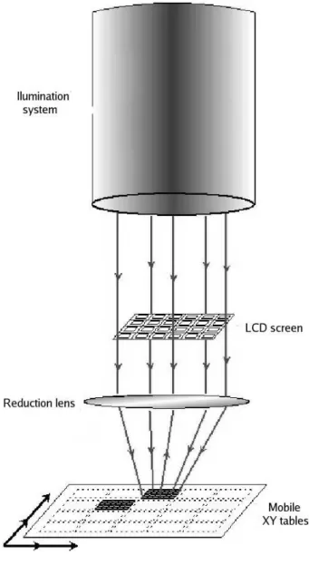
The prototype parallel photoplotter is essentially built of an SLM, projection lens and
a XY table. The basic photoplotter schema is shown in figure 1. A light source is used to
illuminate an SLM and the pattern displayed on the SLM is imaged onto the substrate
by the projection lens. The data content of a typical plot is usually much greater than
the number of pixels on an SLM so a block plotting technique is generally used. Once
the first SLM pattern has been exposed, the illumination is blanked out, the XY table
on which the substrate is placed moves, the next image block is sent to the SLM, the
illumination system unblacked and so on until all of the data has been plotted.
2.2
Overall system design
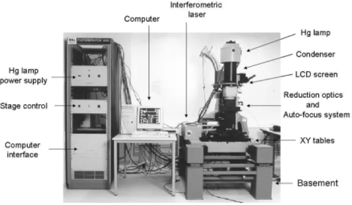
The prototype parallel photoplotter we have built is based on a GCA 4800DSW
photorepeater with a 5 times reduction factor lens. Although more modern photolithographic
steppers and photorepeaters offer a higher performance, as is described below, several
features of this photorepeater (and also of similar photorepeaters) make it particularly
adapted to use with currently available, low cost standard LCD SLMs. As is also shown
below, steppers/photorepeaters of this generation have a very respectable performance
even by today’s standards and especially a high performance/cost ratio. The GCA
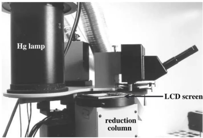
photorepeater converted into the prototype photoplotter is shown in figure 2. Figure
3 shows the drop-in SLM module at the top of the reduction column. The advantages
2.3
Illumination System
The illumination system is an important component of all photolithographic systems.
Here the light source is a mercury arc lamp giving a power of 7.5 mW/cm2 over 10×10
cm2 reticle area with a very high degree of uniformity: ±1% across the reticle area. At
present only a small part of this area is used because of the small size of currently available
SLMs with the required pixel size. As display technology progresses this large area and
uniformity will allow us to use a larger, higher pixel count screen than our current screen
without having to change the illumination system. The fact that the screen only uses the
central reticle area also improves the resolution performance slightly since the performance
of the projection lens is greater near the centre.
We chose an illumination wavelength of 436 nm (g-line) to avoid absorption in the
SLM and because of the availability of high sensitivity photoresists for both binary
and multilevel work at this wavelength. The use of wavelengths below about 400 nm
is problematic when standard LCD are used as the contrast drops (both polarisers and
modulator) and the LC molecules can be damaged by high optical powers at such wavelengths.
Mercury arc lamps cannot be directly modulated so a electro-mechanical shutter is used
to illuminate the LCD screen only when a valid image is present.
2.4
LCD Screen
Driven by the display industry, the characteristics of liquid crystals and LCDs have
been investigated extensively during last decades. The technologies for manufacturing
LCDs are so developed that high-performance and high-resolution LCD panels have
become standard ”off-the-shelf” inexpensive components that can be used as photomasks
for real-time photolithography [11].
(SLM) from TL Electronic GmbH [14] (based on a Sony/Epson panel). It is positioned
using a specially adapted mount on the top of the reduction column with the required
polarisers such that the LC plane is in the same optical plane as a standard photolithographic
reticle. The pixel pitch is square, 33 µm with a rectangular transparent area in the centre
(more details in section 2.8). The screen is a monochrome device with grey level bitmap
images coded on 8 bits, theoretically giving up to 256 grey levels.
The refresh rate of the SLM limits the maximum possible plot rate. The photoplotter
operates at the upper limit of refresh rate with in practice a minimum delay between
successive images of roughly 20 ms: a typical limit for standard nematic LCD like the
one used here. Tests with delays down to 10 ms have produced an unacceptable loss
in contrast and some partial image loss. More modern SLMs, based on FLC, LCOS or
MEMs technology have much faster refresh rates, often of an order or magnitude or more
(details in section 4.1). For our current work the plot rate is not a critical parameter for
this prototype since the plot rate advantage gained by the massively parallel nature of
the SLM means plot rates are already highly respectable.
The PC graphics card is connected to the PC monitor and the SLM via a replicator
which allows us to simultaneously display images on the photoplotter SLM and to verify
them visually on the ordinary monitor.
2.5
Reduction Column
The highly optimised photoreduction lens is the core component of the projection
system and its imaging quality directly influences the plotted characteristics of the patterns
in the photoresist [12]. Our reduction lens is a ZEISS 5x with a numerical aperture of 0.30
giving a 1 µm resolution, over a potential 16×16 mm2 writing field with a total distortion
transparent area as well as the opaque inter-pixel space of the separate SLM pixels whose
exposed area at the photoresist level is approximately 5×3 µm2 on a 6.6 µm pitch.
2.6
XY Tables
The substrate is held on XY table with a vacuum chuck. The XY tables included in
the GCA photorepeater cover a total range of 15×15 cm2using DC motors. To obtain the
required accuracy the tables incorporate electromagnetic tips, the DC motors giving the
long range movement and voice coil motors giving the short range precise positioning using
feedback from a laser based interferometric position detection system with a resolution of
40 nm.
2.7
Electronics and software
Our prototype is based on a GCA stepper built using mainly 1990s technology. As
indicated in the previous section, the optics, mechanics and electronics still offer a very
acceptable performance so there was no need to change them. On the other hand the
original software and the computer hardware (PDP11) is obsolete. We therefore chose to
completely change the plotting module of the photoplotter software but to keep the same
electronics interface because we need the original control electronics. We used a standard
PC with a card from H&L Associates [15] added to directly control the stepper electronics.
We chose to work the Linux operating system because of the ease of manipulation of large
amounts of memory (plot data) and the ease of access to low level graphics routines
bypassing the graphical user interface. A driver to make the interface between the kernel
and the stepper electronics was designed using WinDriver Linux from KRFTech [16].
The new software to control and synchronise the image display on the SLM, the XY
collaboration with MIVA Technologies GmbH [17]. It is important that the photoplotter
accepts the different file formats used in the photoplotting industries in general. Since
the SLM is pixelised, the internal data representation is fundamentally bitmap however
software has been written to enable the photoplotter to accept vectorial image formats
(Gerber and GDSII, DXF via translators). The photoplotter converts these formats into
an internal Run Length Encoded (RLE) format. It can take this internal RLE format,
read it and put the image in the PC RAM as a pixmap. This is then used by the image
display software. As a result the photoplotter can plot binary and grey-level images with
bitmap formats (PGM, TIF, PCX, BMP, . . . ) or binary plot data in vector formats (RLE
directly and Gerber, DXF, GDSII, PostScript, . . . after translation).
2.8
Image display
The limited number of pixels and the less than 100% fill factor of the SLM along
with the requirement that the same hardware should be used to plot large binary 2D
structures and multilevel 3D structures have led to some more sophisticated plotting
techniques being developed. The corresponding software was written to correctly cut and
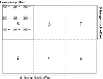
display the image to be plotted into screen-sized blocks to be sent to the SLM. The basic
principles and reasons for these techniques which we term block plotting, super-resolution,
step-and-repeat and multilevel plot will now be described briefly.
- Block Plotting Technique: If the plot data is large it cannot be plotted with one
SLM exposure. It has to be plotted by a block-by-block technique. We extract and
plot a part of the overall plot data, called a block image whose size equals the SLM
size. Then the stages are moved to the next block position, a new image displayed
and so on until the whole pattern has been exposed (see figure 4). In this way the
SLM size.
- Super-Resolution (SR) Technique: Due to the less than 100% fill factor of
SLM pixels and the high resolution of the reduction lens, the surface etched in
the photoresist is not flat: the opaque inter-pixel gap (corresponding to insulating
tracks, transistors for the LCD active matrix, . . . ) is unexposed during the illumination.
After development, this area is unetched in the photoresist while the transparent
pixel centre, exposed during the illumination, is etched down to the substrate after
development. Figure 5 shows such a view of a part of the SLM pixel array exposed
in the photoresist.
In order to resolve this problem we have developed a so-called “super-resolution”
technique. Data are plotted by displaying several successive images onto the SLM
and performing very small translations, by distances that are a fraction (e.g. 1/6 th)
of the pixel pitch, of the XY tables between each exposure. This effectively fills in
the unexposed areas by overlapping the active areas of the different images sent to
the SLM. This “super-resolution” (SR) is performed in both the X and Y directions.
We generally use a factor 6 super-resolution in both directions giving 36 successive
exposures which also eliminate the “staircase” pixelisation effect on diagonal or
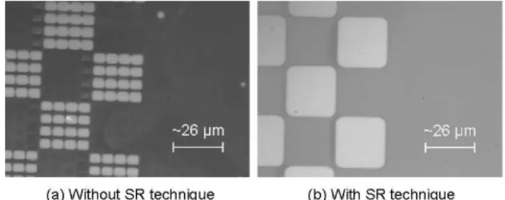
curved plot patterns. Comparison between patterns etched in photoresist with and
without the SR technique is shown on figure 6.
- Step-and-Repeat: To reduce plot data file size, the software also allows for any
image to be repeated using a “step-and-repeat” technique: the pattern is plotted,
the stages move and the same pattern is replotted alongside on a regular matrix.
This feature is particularly useful for plotting structures such as lenslet arrays or
- Multilevel Plot: Etching 3D data with several different etch depths is done by
exposing the photoresist for different lengths of time, the deeper levels being exposed
longer than the more superficial levels. This type of multilevel plot could also be
performed using the grey levels of the SLM: the lower the grey level in the data
image (closer to 0 level), the darker the SLM pixel and the less exposed in the
photoresist. However with many SLMs and in particular with the SLM we use,
the grey levels are designed for image display and therefore adapted to the human
eye so are difficult to control photometrically. As a result we decided to work with
exposure time and successive binary images.
To simplify and increase the speed of the operation, rather than separating the grey
level image into a series of binary images, only one grey level bitmap (coded on
8 bits, so giving up to 256 grey levels) is sent to the SLM and the video palette
changing routines of the video card are used to control how these images appear as
full contrast black and white images on the SLM. Changing the palette is a much
simpler and quicker operation than rewriting a whole SLM image, the appearance
of the image displayed on the SLM changes in one video cycle so blanking with the
mechanical shutter between the different binary versions of the grey level image is
not required. This produces a significant increase in overall plot rate: the limiting
factor is the relatively fast SLM refresh rate and not that of the slower mechanical
shutter. The exposure dose for each level is determined from a look up table (LUT)
which is obtained from a calibration of the photoresist’s photochemical response.
Once this is calibrated it becomes possible to “sculpt” photoresist almost at will to
fabricate a very wide variety of 3D shapes. (see section 3.3).
the plot data are assembled into data images sent to the SLM.
- Initialisation: read plot data file (see section 2.7 for formats), convert to bitmap,
calculate the number of image blocks.
- Image block loop (α, β, γ, ... )
– Super-resolution loop (A, B, C, ...)
∗ Move XY tables to correct position determined by image block and
super-resolution indices.
∗ Assemble image to be sent to SLM screen by selecting pixels from the plot
data bitmap determined by image block and super-resolution indicated in
figure 4.
∗ Send image to SLM, open shutter, expose each grey level for required time
based on photoresist calibration LUT.
– Close super-resolution loop.
- Close image block loop.
2.9
Photoresist
In our experiments we use the SHIPLEY S1800 photoresist series in layers ranging
from a few hundred nm to a few microns. This resist is most sensitive at wavelengths
near 436 nm but can be used between 350 and 450 nm. After exposure, the resist is
developed for 2 min, using the MICROPROSIT 303 developer diluted 1:12 with de-ionized
water. This developer and dilution were chosen to give a relatively linear etch depth as a
function of exposure characteristic [18]. Once suitable development parameters (dilution
and development time) have been determined they are fixed and only the exposure time
3
Experimental Results
3.1
System Alignment
When setting up a stepper, several alignment steps have to be performed to obtain the
specified performance: focus, parallelism of the reticle and XY table planes (out-of-plane
angle), alignment of reticle axes with the XY table translation axes (in-plane angle) and
XY table step distances. We first setup the photoplotter as a conventional stepper and
followed the standard manufacturer’s alignment procedure with a test reticle. We then
adapted the standard reticle-based alignment procedure for use with our reconfigurable
SLM reticle, making a series of test exposures as described below. All these alignment
steps were performed without the super-resolution technique in order to better judge focus
and alignment between successive image blocks. The test image used was either an all
white image (all SLM pixels in the ”on” state) or a specifically designed test pattern.
The first procedure is the adjustment of the auto-focus system which is adjusted
manually as for a test mask reticle until the shape of the SLM pixels is as clear as possible
in the centre of the optical field of view in the test plots (see figure 5). This effectively
ensures that the SLM LC layer is in the object plane of the projection lens and the image
plane coincides with the reference plane of the stepper system’s built-in autofocus system.
This alignment is set once, after which the autofocus system automatically compensates
for different substrate thicknesses and planarity defects. The typical depth of field of this
type of stepper is around a few microns.
The out-of-plane angle alignment is also adjusted once. It consists in placing various
calibrated thickness metal shims in the SLM mount and performing test exposures until
well focused SLM pixels are obtained simultaneously for all corners of the SLM.
be verified every time the prototype changes from stepper mode to photoplotter mode.
However, once the SLM is aligned and fixed in its mount, this is a very quick procedure
as alignment marks are included in the SLM mount which then can be aligned like any
new reticle. The initial alignment is performed by exposing one all white SLM pattern,
translating the stages in the X direction by a distance equal to the SLM size at the
substrate level and exposing another all white pattern. This procedure is then repeated
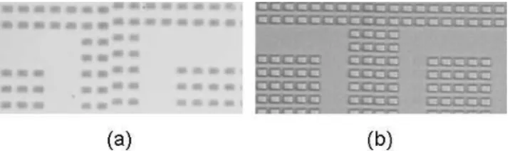
in the Y direction. When the in-plane angle is incorrectly adjusted a gap appears between
the pixels of the successively exposed SLM patterns (fig. 7). When the angles (and the
translation distances) are correctly adjusted the join between different etched SLM blocks
is no longer visible. Figure 8 indicates an angular alignment better than 1/3 pixel (less
than 1 µm) over a field of 800 pixels. More sophisticated, vernier based techniques would
allow a further improvement in alignment precision but for our present applications the
precision of these simple visual alignments is sufficient.
3.2
Binary Direct Write
Binary direct write consists in sending binary images to the SLM and exposing for
durations such that areas of photoresist corresponding to an illuminated SLM pixel are
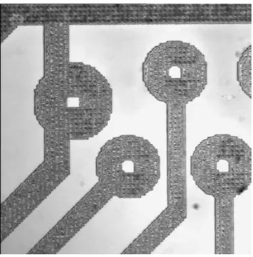
removed completely down to the substrate when developed. Figure 9 and 10 shows the
effectiveness of the photoplotter in binary direct writing. As mentioned above, the SR
technique is used to fill in the “gaps” corresponding to the opaque “dead zone” between
the SLM pixels. Figure 11 shows the resulting pattern in the photoresist. This, however,
produces a problem, always present when the address grid is finer than the writing spot
size: written structures are wider than desired. The net effect is to produce what is
referred to in the binary image processing field as an image “dilatation”. The solution is
required amount.
The number of pixels to be eroded depends on the SLM pixel size and the SR factor.
If S is the pixel size, P the pixel pitch, SR the SR factor and A=P/SR the addressing
grid pitch, N white pixels on the plot data should lead to a N x A etched distance in the
photoresist. With the SR principle N white pixels on the image lead to a N x A + (S
-A) etched distance. The difference between the desired and obtained distance is therefore S - A which means an erosion of (S - A)/A pixels is required. As the pixel number has
to be an integer, we take the nearest integer as the number of eroded pixels. Pictures of
binary lines etched in photoresist without erosion and with erosion are shown in figures
12 (a) and (b). Demonstrating the effectiveness of the technique.
3.3
Multilevel Direct Write
Until recently complex 3D structures have generally been made with expensive and
time-consuming multi-layer photolithographic techniques or slow, single beam direct write
techniques. The use of grey-level SLMs and more especially time multiplexing techniques
opens the possibility to writing multilevel structures into photoresist in a single exposure
step.
In our experiments, in general 8 different levels were etched. Tests were also made
successfully at 16 levels. The present limitation on the number of etched levels is imposed
by the SLM refresh rate: for fixed resist thickness and development parameters the higher
the number of levels the shorter the time each individual binary image present on the SLM
must be exposed. At 16 levels the required image display duration was under 20 ms which
is the practical limit for the nematic based LCDs used here. More levels could be produced
by either using a faster SLM (see section 4.1) or by reducing the light power. The second
In practice, in many cases 8 levels are usually sufficient since when used with large
SR factors, the write pixels overlap because the width of the writing pixel covers several
address grid points and hence an overlap of light from neighbouring points occurs. This
produces a smoothing effect which leads to practically continuous relief profiles such as
those shown in figure 13.
A wide range of 3D structures including cones, pyramids and circular, elliptic, spherical
or aspherical microlenses have been realised with the multilevel direct writing technique.
Figure 14 shows an example of the sort of structures that can be written by multilevel
direct write. Figure 15 demonstrates the level of control that has already been achieved:
a vertical resolution of better than 50 nm into 1 micron photoresist layers. Through use of
suitably designed calibration tables we were also able to direct write binary and multilevel
structures side by side on the same substrate in the same exposure step.
3.4
Resolution
The minimum feature size of plotted structures is determined by the lens reduction
factor and the SLM pixel size. With our SLM and the 5× reduction lens, the minimal
feature size written in the photoresist is the photoreduced pixel size 5×3 µm2corresponding
to the transparent central part of the SLM pixel. However through the use of the high
resolution XY tables and the SR technique it is possible to apply a much smaller address
grid as the XY tables can make steps down to 40 nm. We typically use a 1.1 micron address
grid. By suitable preparation of the plot data files and allowance for the “dilatation”
effect mentioned above, it is possible to produce “unetched” binary structures down to
the optical resolution of the system, here about 1 µm - see fig. 16. As an illustration,
an uncompensated data file with a 1 micron address grid containing 1 pixel vertical lines
to the 5 micron width of the SLM pixels. Hence with our present system in a positive
resist we can build 1 µm structures with 3 or 5 µm gaps. In a negative resist we can build
3 to 5 µm structures with 1 µm gaps.
3.5
Plot Rate
On the present prototype a binary pattern of 600x800 pixels (entire SLM) giving a
6.6 µm photoresist level pixel pitch is plotted with an exposure of less than 200 ms which
gives a basic 2.4 Mpixels/s or 2.9 mm2/s plot rate. For multilevel structures exposure
time and hence plot rate depend on the local structure etch depths - typically exposure
steps of about 20 ms per layer are required giving overall plot rates that are relatively
similar to the binary case. Super-resolution translation distances are very short so do not
greatly reduce the overall plot rate. The translations between the different image blocks,
however, are greater and do reduce overall plot rate. Exact rates obtained depend on plot
data but typical average values are of the order of a cm2/min.
4
Discussion
The current performance of the photoplotter described above is already competitive
in terms of plot rate and resolution in a number of the application fields mentioned in the
introduction, particularly in terms of cost and flexibility. However, the performance can
also be improved relatively simply. We now discuss the current and more fundamental
limitations on photoplotters based on SLM reticles for photolithographic steppers and
4.1
Plot rate
The plot rate can be improved in 3 major ways. The first and simplest is to use
more recent LCDs with higher pixel counts: compatible 1024x768 and 1280x1024 pixels
LCDs are now commercially available and even higher, HDTV driven, pixel counts now
appearing or planned. The maximum refresh rates of these new microdisplays are at least
as high as our current SLM so factor three to four increases in plot rate are immediately
available for very minor modification to the system. In addition, as LCD microdisplay
technology progresses in the future, plot speed will be increased accordingly, the only
change being required in the photoplotter is a modified LCD mount and when necessary
a more recent video card.
The second way to improve plot rate also concerns the SLM. The current plot rate is
limited by the maximum display rate on the LCD. By using recent, alternative, commercially
available microdisplay technologies such a Liquid Crystal on Silicon (LCOS) [19], Ferroelectric
Liquid Crystal (FLC) [20, 21] and Texas Instrument’s Digital Micromirror device (DMD)
light modulator, technologies significantly higher refresh rates could be achieved. LCOS
is a reflective technology where liquid crystals are present over the surface of a silicon
chip coated with a reflective aluminized layer. The opaque inter-pixel space is greatly
reduced because the control circuit is in the silicon backplane, thus increasing optical
efficiency. The close link between drive electronics and each pixel also greatly simplifies
image update often resulting in significantly improved display refresh rates. FLC devices
use liquid crystal substances that have chiral molecules in a smectic C arrangement and
allow microsecond switching times - often more than an order of magnitude faster than
nematic LC based devices. DMD technology consists of hundreds of thousands of moving
micromirrors which are controlled by underlying CMOS electronics [12, 13]. Such devices
The practical use of such technologies is, however, not as straightforward as using
higher pixel count transmissive LCDs. These new technologies are reflective so a major
redesign of the display illumination system would be required. Another practical difficulty
concerns getting the plot data onto the devices quickly enough to be able to access such
high refresh rates. Standard video cards are designed for the human eye so generally have
maximum refresh rates in the 100 Hz range. Custom designed drive electronics are now
appearing for some devices but they are very significantly more expensive. Currently the
best compromise appears to be to use mass market PC video cards and drivers which
allow maximum refresh rates in the 100 Hz range. By using the three colour channels
(RGB) to each display monochrome plot data, the effective refresh rate can be tripled.
The other practical difficulty is that if such refresh rates can be achieved, plot rate will
then be limited by available light power. The reflective technologies help in this direction
as they generally have higher fill factors and hence optical efficiency. However, with our
current system, refresh rates in excess of 100 Hz (corresponding to a 10 ms display time for
a given etch depth level in a multilevel plot) would again require an illumination system
redesign with a higher power light source and perhaps a different light source such as a
pulsed laser, adding considerable complexity and expense.
The third, linked, technique for increasing plot rate is to use “on-the-fly” plotting in
which the XY tables move continuously. This would remove the need to wait for the
tables to reach the desired position and stabilise before exposing each SLM image. In this
way the full refresh rate of the SLM could be used at all times, significantly increasing the
overall plot rate. The application of “on-the-fly” plotting, however, would entail a major
modification of the current system since a high power, short duration, pulsed source would
be required along with redesigned XY table drive electronics and software to be sure of a
pulse power would also have to be addressed. These factors would make the reuse of
existing steppers much more complicated: a complete system redesign would be required,
greatly increasing costs and losing the advantages of the approach proposed here.
4.2
Resolution
As indicated above, the smallest feature size of plotted structures (3x5 micron structures
with 1 micron gaps) is limited by the lens reduction factor and the SLM pixel size. The
resolution can be improved simply in two ways: using an SLM with smaller pixels and
using a lens with a greater reduction factor.
As SLM pixel count has increased in recent devices, the pixel size has tended to
decrease so simply replacing the existing SLM with a more recent one would improve
both the plot rate and resolution. Typical current transmissive LCD microdisplays of the
type mentioned in section 4.1 have pixel pitches of 15-20 µm with active areas of around
10-15 micron giving a roughly factor two gain in minimum feature size. Reflective LCOS
or DMD generally have significantly smaller pixels (less than 10 µm for the most recent
LCOS devices, giving improved resolution at the expense of a redesigned illumination
system).
Changing lens reduction factor is also a relatively simple way to increase resolution
as 10:1 and 20:1 reduction factor lenses already exist for the type of stepper used as the
basis for our photoplotter. Thus by combining smaller SLM pixels and available reduction
factor lenses it is relatively simple to reach resolutions limited by the resolving capabilities
of the reduction lens - roughly 1 µm for the g-line steppers compatible with LCD SLMs.
Going to features sizes smaller than this would require the use of lenses optimised
for shorter UV wavelengths (for example i-line). This, however, is problematic with
compatible polarisers are more difficult to find at these wavelengths. To be able to use such
wavelengths other SLM technologies such as DMD are required, which in turn means the
stepper illumination system would have to be redesigned to take account of the reflective
display - again losing many of the advantages of the approach proposed here.
5
Conclusion
In this paper we have shown that, by combining a standard transmissive liquid crystal
microdisplay with an existing g-line photolithographic stepper, a highly versatile
direct-write photoplotter can be built simply and relatively cheaply. The resulting system has
a respectable performance as a photoplotter in terms of resolution, plot rate and cost. In
addition, thanks to the drop-in nature of the microdisplay module, the photoplotter can be
simply converted to a standard stepper in a few minutes. As such it is particularly adapted
for R&D labs and custom or short production runs. The same equipment can be used
for both binary plots (e.g. for chrome photomask fabrication) and for the production of
3D microstructures by grey-level, direct write into photoresist. The only change between
these two operating modes is the control software, indeed the simultaneous plotting of
binary and multilevel data on the same substrate has also been demonstrated. The
present performance can be very easily improved in both resolution and plot rate thanks
to ongoing improvements in LCD technology. We have discussed the current limitations
on the approach and proposed ways of overcoming them.
Our current work in the field is centred on improving the resolution performance in
two separate ways. The first involves a new prototype based on the same principle and
software but with a stronger reduction factor lens and a reflective micromirror device in
of proximity correction techniques on the plot data. The surface relief obtained with the
photoplotter can be modelled as the convolution of the point-spread function (PSF) of
optical instrument with the desired relief profile which would have been obtained in the
absence of this smoothing effect [18, 22, 23]. This technique is well known in single beam
direct write applications and several techniques exist for precompensating the plot data to
correct for this smoothing and hence obtain plots closer to the desired profile [18, 22–27].
Adaptation of these techniques to our massively parallel photoplotting technique with
our non-standard write beam profiles and individually variable power levels is already
showing promising results and will be presented in a future paper.
Acknowledgements
This research was mainly funded by EC through the CRAFT DRAWMAP project. We
also acknowledge the contribution of PM Professional Maintenance in setting the stepper
and Carole Moussu and Andreas Weber in the initial stages of this work.
References
[1] M. B. Stern, ”Binary optics fabrication,” Chap. 3 in Micro-optics: elements, systems
and applications, H. P. Herzig, pp. 53–86, CRC Press, Cornwall (1997).
[2] N. Dumbravescu, ”Experiments for 3-D structuring of thick resists by gray tone
lithography,” Materials Science in Semiconductor Processing, 3, 569–573 (2000).
[3] H. Yu, B. Li, and X. Zhang, ”Flexible fabrication of three-dimensional multi-layered
microstructures using a scanning laser system,” Sensors and Actuators A, 125, 553–
[4] N. Matsuzuka, Y. Hirai, and O. Tabata, ”A novel fabrication process of 3D
microstructures by double exposure in deep x-ray lithography (D2XRL),” J.
Micromech. Microeng., 15, 2056–2062 (2005).
[5] N. Yamazaki, T. Yamaguchi and H. Namatsu, ”Three-dimensional nanofabrication
with 10-nm resolution,” Jpn. J. Appl. Phys., 43(8B), 1111–1113 (2004).
[6] T. Osipowicz, J. A. van Kan, T. C. Sum, J. L. Sanchez, and F. Watt, ”The use
of photon microbeam for the production of microcomponents,” Nucl. and Meth. B,
161-163, 83–83 (2000).
[7] H. Martinsson, T. Sandstrom, A. Bleeker, and J. D. Hintersteiner, ”Current status
of optical maskless lithography,” J. Microlith., Microfab., Microsyst., 4(1), 011003
(2005).
[8] R. Menon, A. Patel, D. Gil, and H. I. Smith, ”Maskless lithography,” Materials
Today, 8, 26–33 (2005).
[9] M. T. Gale, M. Rossi, H. Sch¨utz, P. Ehbets, H. P. Herzig and D. Prongu´e,
”Continuous-relief diffractive optical elements for two-dimensional array generation,”
Appl. Opt., 32(14), 2526–2533 (1993).
[10] F. Nikolajeff, S. Jacobsson, S. H˚ard, ˚A. Billman, L. Lundbladh and C. Lindell,
”Replication of continuous-relief diffractive optical elements by conventional compact
disc injection-molding techniques,” Appl. Opt., 36(20), 4655–4659 (1997).
[11] Q. Peng, S. Liu, Y. Guo, B. Chen, J. Du, and Y. Zeng, ”Real-time photolithography
technique for fabrication of arbitrarily shaped microstructures,” Opt. Eng., 42(2),
[12] Y. Gao, T. Sheng, J. Chen, N. Luo, X. Qi, and Q. Jin, ”Research on high-quality
projecting reduction lithography system based on digital mask technique,” Optik,
116, 303–310 (2005).
[13] L. Chi, G. Xiaowei, G. Fuhua, L. Boliang, D. Xi, D. Jinglei, and Q. Chuankai,
”Imaging Simulation of Maskless Lithography Using a DMDTM,” Proc. SPIE, 5645,
307–314 (2005).
[14] TL Electronic GmbH, http://www.tl-electronic.de/
[15] H&L Associates, http://www.trilicium.ca/hl index.php/
[16] KRFTech ltd. changes names to Jungo ltd., http://www.jungo.com/
[17] MIVA Technologies GmbH, http://www.mivatec.com/
[18] P. Ehbets, M. Rossi, and H. P. Herzig, ”Continuous-relief fan-out elements with
optimized fabrication tolerances,” Opt. Eng., 34(12), 3456–3463 (1995).
[19] K. M.Johnson, D. J. McKnight, and I. Underwood, ”Smart spatial light modulators
using liquid crystals on silicon,” IEEE Journal of Quant. Electr., 29(2), 699–714
(1993).
[20] Displaytech Inc., http://www.displaytech.com/
[21] Forth Dimension Displays Ltd., http://www.crlopto.com/
[22] J. Bengtsson, ”Direct inclusion of the proximity effect in the calculation of
kinoforms,” Appl. Opt., 33(22), 4993–4996 (1994).
[23] M. Ekberg, F. Nikolajeff, M. Larsson, and S. H˚ard, ”Proximity-compensated blazed
transmission grating manufacture with direct-writing, electron-beam lithography,”
[24] L. Grella, E. Di Fabrizio, M. Gentili, M. Baciocchi, and R. Maggiora,
”Proximity correction for e-beam patterned sub-500nm diffractive optical elements,”
Microelectron. Eng., 35, 495–498 (1997).
[25] H. Zhang, J. Morrow, and F.M. Schellenberg, ”Optical proximity correction: a detail
comparison of techniques and their effectiveness,” Microelectron. Eng., 41/42, 79–82
(1998).
[26] J. Du, Q. Huang, J. Su, Y. Guo, and Z. Cui, ”New approaches to optical proximity
correction in photolithography,” Microelectron. Eng., 46, 73–76 (1999).
[27] L. Veneklasen, U. Hofmann, L. Johnson, V. Boegli, and R. Innes,
”Run-time correction of proximity effects in raster scan pattern generator systems,”
Microelectron. Eng., 46, 191–195 (1999).
Biographies
M´elanie Kessels received her University degree and her M.Sc. in Physics Sciences
from the University of Li`ege (BELGIQUE) in 2003 and 2005, respectively. She is presently
working towards the Ph.D. degree in Engineering Sciences at the Ecole Nationale Sup´erieure
des T´el´ecommunications de Bretagne (E.N.S.T.) in Brest (FRANCE).
Dr. Kevin Heggarty received his B.A. in Natural Sciences from the University of
Cambridge (UK) in 1987, his M.Sc. in Telecommunications and Information Systems
from the University of Essex (UK) in 1988 and his doctorate from the Ecole Nationale
Sup´erieure des T´el´ecommunications (E.N.S.T.) in Paris (FRANCE) in 1991. He is now
senior lecturer at the ENST Bretagne. His research interests include non-display applications
List of Figures
1 Parallel write photoplotter basic principle. Illumination system illuminates
the LCD. The LCD is imaged onto photoresist coated substrate with a
reduction factor lens. . . 28
2 GCA 4800DSW photorepeater converted into a photoplotter. . . 29
3 Microdisplay mounted on the photorepeater. The SLM module is positioned
using a specially adapted mount on the top of the reduction column such
that the LC plane is in the same optical plane as a standard photolithographic
reticle. . . 30
4 “Block plotting” and “super-resolution” principle. The plot data is cut
into 6 blocks (α, β, γ, δ, ε and φ) whose size equals the SLM size. The first
block α is plotted using the “super-resolution” technique. At the moment
of the first illumination, the pixels A are displayed on the SLM, then the
pixels B, then C, . . . until the whole block α is plotted. The same steps are
used to plot block β, then block δ, . . . . . . 31
5 Photograph of a part of the pixel array etched into photoresist corresponding
to an LCD screen where all pixels are in the ON state (transparent). . . . 32
6 Comparison between etched patterns (a) without and (b) with the SR
technique. In (a) LCD screen pixels are visible. In (b) the SR technique
eliminates the pixelisation effect. . . 33
7 The relative angle between the XY stages and the screen must be adjusted.
(a) Bad relative angle adjustment: pixels on the block boundaries are badly
aligned. (b) Relative angle is adjusted: block boundary etched screen pixels
8 A test file is used to verify screen alignment: auto-focus, angular alignment
and junction between etched screens. . . 35
9 View of a binary direct-write plot in photoresist from a PostScript file. . . 36
10 A 3D view of a directly written grating in photoresist obtained using an
interferometric microscope. A flat surface in the upper unexposed areas and
in the lowest level areas (indicating complete removal of the photoresist)
and steep edges between the 2 flat surfaces are visible. . . 37
11 When plotting binary images with the SR technique, successive exposures
etch the desired image in the photoresist. Between the successive exposures,
the substrate moves. Each photoresist area is exposed differently as a
function of the number of received exposures. In this example, the photoresist
has been exposed to 3 SLM patterns. The pixel overlap areas have been
exposed three times. The different grey levels code different etch depths.
The darker the area, the more illuminated and then the more exposed in
the photoresist. . . 38
12 Pictures of binary lines etched in photoresist (a) without erosion and (b)
with erosion shown. Etched and non-etched lines should be of 5 µm width.
(a) When the image to be plotted is not precompensated, the etched
lines are larger than the non-etched lines. (b) When lines are correctly
precompensated on the image to be plotted, etched and non-etched lines
are of equal width as desired. . . 39
13 A 3D view of continuous relief diffractive structure obtained by direct write.
14 A 2D interferometric microscope plot of different shapes simultaneously
directly written into photoresist. The different grey levels code different
etch depths. . . 41
15 A 2D slice through a multilevel staircase diffraction grating obtained by
direct write into photoresist showing a depth control precision better than
50 nm. . . 42
16 By using the SR technique it is possible to use a much smaller address grid
(here 1.06 µm) and hence leave gaps between “written” structures of down
to 1 µm. On this figure, horizontal etched 8 µm width lines with 2 µm
unetched gaps and, vertical etched 9 µm width lines with 1 µm unetched
Figure 1: Parallel write photoplotter basic principle. Illumination system illuminates the LCD. The LCD is imaged onto photoresist coated substrate with a reduction factor lens.
Hg lamp
reduction column
LCD screen
Figure 3: Microdisplay mounted on the photorepeater. The SLM module is positioned using a specially adapted mount on the top of the reduction column such that the LC plane is in the same optical plane as a standard photolithographic reticle.
Figure 4: “Block plotting” and “super-resolution” principle. The plot data is cut into 6 blocks (α, β, γ, δ, ε and φ) whose size equals the SLM size. The first block α is plotted using the “super-resolution” technique. At the moment of the first illumination, the pixels A are displayed on the SLM, then the pixels B, then C, . . . until the whole block α is plotted. The same steps are used to plot block β, then block δ, . . .
Figure 5: Photograph of a part of the pixel array etched into photoresist corresponding to an LCD screen where all pixels are in the ON state (transparent).
Figure 6: Comparison between etched patterns (a) without and (b) with the SR technique. In (a) LCD screen pixels are visible. In (b) the SR technique eliminates the pixelisation effect.
Figure 7: The relative angle between the XY stages and the screen must be adjusted. (a) Bad relative angle adjustment: pixels on the block boundaries are badly aligned. (b) Relative angle is adjusted: block boundary etched screen pixels are aligned.
Figure 8: A test file is used to verify screen alignment: auto-focus, angular alignment and junction between etched screens.
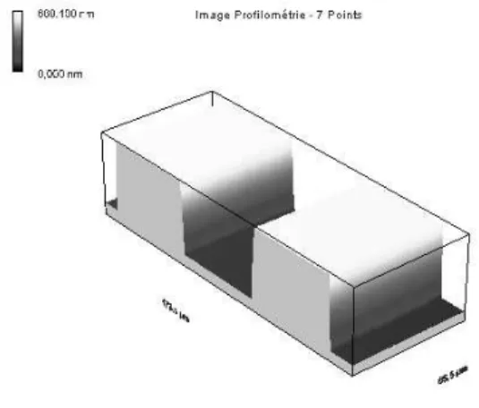
Figure 10: A 3D view of a directly written grating in photoresist obtained using an interferometric microscope. A flat surface in the upper unexposed areas and in the lowest level areas (indicating complete removal of the photoresist) and steep edges between the 2 flat surfaces are visible.
Figure 11: When plotting binary images with the SR technique, successive exposures etch the desired image in the photoresist. Between the successive exposures, the substrate moves. Each photoresist area is exposed differently as a function of the number of received exposures. In this example, the photoresist has been exposed to 3 SLM patterns. The pixel overlap areas have been exposed three times. The different grey levels code different etch depths. The darker the area, the more illuminated and then the more exposed in the photoresist.
Figure 12: Pictures of binary lines etched in photoresist (a) without erosion and (b) with erosion shown. Etched and non-etched lines should be of 5 µm width. (a) When the image to be plotted is not precompensated, the etched lines are larger than the non-etched lines. (b) When lines are correctly precompensated on the image to be plotted, etched and non-etched lines are of equal width as desired.
Figure 13: A 3D view of continuous relief diffractive structure obtained by direct write. The smooth surface is obtained thanks to a high SR factor.
Figure 14: A 2D interferometric microscope plot of different shapes simultaneously directly written into photoresist. The different grey levels code different etch depths.
Figure 15: A 2D slice through a multilevel staircase diffraction grating obtained by direct write into photoresist showing a depth control precision better than 50 nm.
Figure 16: By using the SR technique it is possible to use a much smaller address grid (here 1.06 µm) and hence leave gaps between “written” structures of down to 1 µm. On this figure, horizontal etched 8 µm width lines with 2 µm unetched gaps and, vertical etched 9 µm width lines with 1 µm unetched gaps are plotted.