HAL Id: hal-00385694
https://hal.archives-ouvertes.fr/hal-00385694
Submitted on 19 May 2009
HAL is a multi-disciplinary open access archive for the deposit and dissemination of sci-entific research documents, whether they are pub-lished or not. The documents may come from teaching and research institutions in France or abroad, or from public or private research centers.
L’archive ouverte pluridisciplinaire HAL, est destinée au dépôt et à la diffusion de documents scientifiques de niveau recherche, publiés ou non, émanant des établissements d’enseignement et de recherche français ou étrangers, des laboratoires publics ou privés.
ESD Induced Latent Defects In CMOS ICs And
Reliability Impact
Nicolas Guitard, David Trémouilles, Stéphane Alves, Marise Bafleur, Félix
Beaudoin, Philippe Perdu, Alain Wislez
To cite this version:
Nicolas Guitard, David Trémouilles, Stéphane Alves, Marise Bafleur, Félix Beaudoin, et al.. ESD Induced Latent Defects In CMOS ICs And Reliability Impact. Electrical Overstress and Electrostatic Discharge (EOS/ESD) Symposium, Sep 2004, Dallas, United States. pp.174-181. �hal-00385694�
ESD Induced Latent Defects In CMOS ICs And
Reliability Impact
N. Guitard (1), D.Trémouilles (1), S.Alves (1), M.Bafleur (1), F.Beaudoin (2), P.Perdu (2),
A.Wislez (3)
(1) LAAS-CNRS, 7 av. Colonel Roche - 31077 Toulouse Cedex 04 (2) CNES-THALES, 18 av. Edouard Belin, 31401 Toulouse (3) LCIE, 18, avenue Edouard Belin 31401 Toulouse Cedex
Abstract – A dedicated test vehicle was designed to study the impact of ESD induced latent defects on digital
and analog CMOS circuits. Both CDM and TLP stresses were applied to these circuits through a specific pad which allows stressing the circuit core. Both electrical characterization and non-destructive failure analysis were performed to locate the induced defect. For digital circuits, functionality is not affected although the IDDQ quiescent current increased. However, after burn-in and storage, it was observed that the IDDQ current significantly increased suggesting that the circuit lifetime is degraded. In contrast, even at very low stress level, the analog circuit exhibits a dramatic offset degradation and no recovery is observed after burn-in.
I. Introduction
Given the evolution of MOS technologies, electrostatic discharge (ESD) will become one of the major causes of yield and reliability issues of future integrated circuits. Nowadays, the main difficulties are related to the drastic design constraints of ESD protection structures: first, the reduced design margins defined by the respective breakdown voltage values of gate oxides and junctions and second, the requirement for low parasitics and smaller silicon area. As a consequence, the risk for ESD damage in the circuit core increases for both Human Body Model (HBM) and Charged Device Model (CDM) events.
"" 1µA 0 0,5 1 1,5 2 Discharge voltage (kV) 10-3 10-4 10-5 10-6 10-7 10-8 10-9 10-10 10-11 10-12 Leakage Current @5V (A) 10nA
Ideal
Ideal
latent defect? latent defect?Fig.1: Leakage current of various devices after several ESD stress steps .
ESD qualification usually insures that after a given maximum ESD stress, the circuit is not degraded i.e. functionality and leakage current remain within specifications. As shown in Fig.1, several cases can occur : an abrupt increase of this characteristics (ideal case) or a progressive evolution with stress. Even if a low increase in leakage current is acceptable, its evolution demonstrates the presence of a degradation within the circuit that could develop into a latent defect. Such a defect may evolve during circuit operation and later on result in a field failure.
Moreover, ESD qualification is based on using standards whose representation of the real world could be questionable as analyzed by Hyatt [1]. For example, HBM standard uses a single pulse although in the real world, nearly every ESD event occurs as a pulse train, the latter carrying a much higher energy than the former one. Similar discrepancies are observed for other parameters such as voltage, current and rise time.
As a result, it can be stated [1] that “most electronic equipment tested to standardized methods cannot claim to be fully ESD hardened to environmental ESD”.
For high reliability applications such as the aerospace application, it is important to check that all the components implemented into the system did not undergo any environmental ESD stress that could jeopardize its long term reliability. Actually, to date,
160 malfunctions of equipments in orbit and 5 losses were attributed to environmental ESD [2]. The mean cost of a satellite loss is about $75 million!
To guarantee the ESD robustness of a circuit, one can choose a strict failure criterion based on "no increase" in leakage current. Such a criterion is not efficient in practice since a latent defect only induces nano-amps increase in leakage current that is not detectable in the micro-amps range of the whole IC quiescent current. Understanding how such defects can evolve during the lifetime of a circuit is then essential.
The purpose of this paper is the study of the impact of ESD induced latent defects on CMOS ICs reliability. Previous work [3-4] already studied the impact of ESD stress on circuit reliability. This work is focused on ESD defects intentionally induced into a specific location into the circuit core. To specifically create such defects, we designed a dedicated test vehicle in a 0.6µm mixed-signal CMOS technology that allows stressing a desired element within the circuit. Both CDM and TLP stresses were applied to the circuits. A thorough study of the stressed circuits including electrical characterization, burn-in and failure analysis, is performed.
Fig.2: Electrical schematic of the oscillator circuit. VSTR pin is used to apply the ESD stress on inverter I12.
II. Test Vehicle And Methodology
The main objective of this test circuit is to simulate an ESD stress that is higher than the specified robustness of the circuit thereby resulting in a local overvoltage or overcurrent within the circuit core on the power supply rail.
The technology used is a 0.6µm twin-well mixed-signal CMOS technology with a resistive P-type substrate (25 Ω.cm). In the test vehicle, to specifically induce such an ESD defect into the circuit core, either digital or analog, we designed two types of test circuits that can be stressed directly on a desired element:
− An oscillator that is controlled by a NAND or a NOR input gate (Fig.2). As a result, depending on the IN input signal, this circuit is either an oscillator (IN=1) or an inverter circuit (IN=0). This allows a simple testing set up for both DC and dynamic electrical measurement.
− A simple analog CMOS differential stage (Fig.3).
Fig.3 : Electrical schematic of the analog differential stage. Five different versions of the oscillator are implemented on the test chip to allow stressing a different logic gate within the oscillator: NAND input gate, NOR input gate, inverter within the core of the oscillator, inverter of the buffer stage (Fig.2) and transmission gate inserted into the oscillator loop. For the differential stage, the stressed pin is the VDD power supply one. For the oscillator circuits, the stressed pin, called VSTR, is the connection to VDD power supply of the intentionally stressed logic gate, that is separated from the rest of the circuit power supply (ex: power supply of inverter I12 in Fig.2). As a result, the ESD stress is directly applied to the source of the PMOS transistor of this logic gate. Each test circuit has independent VDD and VSTR pads. However, to reduce the number of pads, they all have a common VSS rail. As we will see hereafter, this floorplan strategy has a strong impact on the way the different circuits are stressed. The final test chip (Fig.4) ended up with 68 pads and was assembled in a ceramic PGA package.
The oscillator circuits underwent CDM stresses using a Socketed CDM Verifier II tester. After charging the packaged test circuit, it is discharged through its VSTR pin. The differential stage was stressed using a TLP setup to allow controlling small step stress. For this latter case, between each step stress, the leakage current of both the stressed gate and the full circuit is
monitored and the stress was stopped as soon as the leakage current increased by a decade.
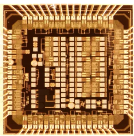
Fig.4 : Optical micrograph of the test chip.
For each reference and stressed oscillator circuit, both DC and dynamic functionality testing is performed before and after stress. For the differential stage, the monitored parameter is its offset. A failure analysis based on electrical measurement, EMMI (EMission MIcroscopy) and OBIRCH (Optical Beam Induced Resistance Change) experiments were carried out to localize the induced failure.
Both reference and stressed chips (samples #1, 3, 6 and 7 from Table 1) were submitted to a burn-in experiment at 85°C during 200h under 5V bias and the electrical DC and dynamic characteristics tested again.
Finally, these devices were stored into their anti-static package during two years at ambient temperature and their electrical characteristics measured again.
Table 1: Results of leakage current and functionality at VDD=4V after the ESD stress testing compared to the reference device, for the oscillator of Fig.2 having the VSTR pad on a buffer inverter.
Sample # 1 3 4 5 6 8 10 CDM stress Ref 10 @ 1.5kV 10 @ 1kV 10 @ 2kV 10 @ 2kV 1 @ 2kV 10 @ 2kV
Leakage current and Functionality right after stress IDDQ (A) 195p 310n 105p 240µ 517n 101p 500µ
ISTR (A) 75p 170n 37p 240µ 500n 31p 500µ
VOUT(V) 3.96 3.96 3.96 3.96 3.96 3.96 3.90
Freq(MHz) 290 300 270 300 270 280 280
Leakage current and Functionality after 2 years of storage IDDQ (A) 8.7m 482n 1.3n 238µ 1.7µ 1.3n 575µ ISTR (A) 8.5m 480n 1.2n 238µ 1.5µ 1.2n 575µ VOUT(V) 1.63 3.97 3.97 3.97 3.97 3.98 3.98 Freq(MHz) 288 288 276 303 280 284 285 Idyn(A) 8.8m 8m 8.34m 9.05m 8m 8.7m 9.2m STATUS Failed OK OK OK OK OK OK
The planned testing procedure consisted of stressing 6 samples of each test circuits (5 versions of the oscillator) at different CDM levels on their VSTR pin, one additional sample is used as reference. The applied CDM stress is such that negative charges are generated within the substrate. For N-well CMOS technologies, this is the most stressful case since for the charges to be evacuated, some junctions should become reverse biased.
The first version of the oscillator under test was the one of Fig.2 having the VSTR pad on one core inverter (I12). The results are presented in Table 1. Table 2: Results of leakage current and functionality at VDD=4V after the ESD stress testing,, for the oscillator having the VSTR pad on its NAND input gate.
Sample # 1 2 3 4 6 7 9 CDM stress Ref 1 @ 2kV 10 @ 1.5kV 10 @ 1kV 10 @ 2kV 1 @ 2kV 1 @ 2kV
Leakage current and Functionality right after stress IDDQ (A) 156p 215p 230µ 270p 3.3m 340p 1.5m
ISTR(A) 84p 35p 230µ 130p 3.3m 100p 1.5m
VOUT(V) 3.96 3.96 3.96 3.96 3.96 3.96 3.96
Freq(MHz) 280 285 290 290 270 280 at “1” Stuck
Leakage current and Functionality after 2 years of storage IDDQ(A) 176p 202p 2.92m 207p 3.6m 343p 1.86m ISTR(A) 53p 57p 2.92m 53p 3.6m 193p 1.86m VOUT(V) 3.96 3.98 3.98 3.97 3.98 3.99 3.98 Freq(MHz) 267 286 292 289 272 275 at “1” Stuck Idyn(A) 8.4m 8.7m 8.8m 8.7m 8.5m 8.6m 1m STATUS OK OK OK OK OK OK Failed
It has to be mentioned here that the planned testing procedure could not be performed as expected. Actually, when we wanted to stress a second type of circuit, we noticed upon measuring the IDDQ and ISTR (on pad VSTR) leakage currents that all of the four others versions of the oscillator, except the reference one, had undergone an indirect CDM stress. This was attributed to the fact that all the test circuits have a common ground rail. Anyway, this indirect stress was interesting to analyze since that was the type of stress we wanted to study. We only present here, in Table 2, the results for the oscillator having a VSTRESS pad on its NAND input gate.
III. Failure analysis
A. Failure localization
Emission microscopy (EMMI) and electrical characterization were used to localize the damaged site right after stress. On the devices under study,
EMMI was able to detect the defect only if the leakage current is in the µA range. As it can be seen in Fig.5, the emission is located into the PMOS transistor of the stressed logic gate. On this picture, the way the VSTR pad is implemented can be noticed: the stressed inverter has separated N-well and connection to the power supply.
Fig.5: EMMI defect localization (circled) in the oscillator of Fig.2 for sample #5.
To define whether this defect originates from a gate oxide breakdown or a molten filament into a junction, we use the access to the VSTR pad to perform corroborating electrical measurements (Fig.6). By applying a varying voltage to the VSTR pad at a constant VDD power supply, it was possible to actually identify the type of defect (gate to source short, drain to source short...).
Fig.6: Electrical measurement set-up used for defect localization in the oscillator of Fig.2. Current leakage path for sample #3. As an example, for the oscillator of Fig.2, the stressed logic gate is the first inverter (I12) of a buffer stage. For DC measurement, we set the input IN of the oscillator to “0”, therefore the input of the stressed gate should be high whereas its output should be low. The measurement procedure is the following: VSTR voltage is set to a constant value, here 5V, and VDD voltage is varied from 3 to 5V and vice-versa. For
each VDD (or VSTR) value, the respective leakage currents IDD and ISTR are measured. By analyzing the way these currents evolve, the type of defect can be identified. In most of the cases, the damage is located into the gate oxide of the PMOS transistor of the stressed cell on the source side that is in good agreement with a CDM failure signature [3]. At higher leakage current level (samples #5 and 10 in Table 1), we could also observe a drain-substrate short.
Regarding the circuits that were indirectly stressed, the failure location was always located into the gate connected to the VSTR pad. It had the same effect as a direct stressing and then allowed using these circuits for the reliability study.
B. Induced Physical Damages
Although the functionality behavior of the stressed devices is similar to the one of non-stressed devices, the question is how to determine if the measured weak leakage currents are related to a physical damage which could evolve into a hard failure after a while. Thermal Laser Stimulation (TLS) such as OBIRCH (Optical Beam Induced Resistor Change [5]) or TIVA (Thermally Induced Voltage Alteration [6]) are non destructive techniques that allows the localization of an ohmic path crossed by a leakage current.
We used these fault localization techniques for the oscillator test circuit of Fig.2 on samples #3, 5, and 6 that have the lowest ISTR leakage current values (Table 1). Sample #3 is an interesting case since the leakage current is in the hundred of nanoamps range.
Fig.7: Dynamic EMMI defect localization (circled) in the oscillator of Fig.2 for sample #3.
The only technique able to detect a defect for this particular case, is the dynamic EMMI i.e. during the operation in oscillator mode. It shows that a defect is located in the source side of the PMOS transistor of the stressed gate (Fig.7). The emission in the NMOS
transistors is the normal emission of the transistors in saturation mode. The electrical measurement via the VSTR pad confirmed that the leakage is induced by a gate oxide breakdown between the gate and the source or/and the N-well substrate (Fig.6).
Regarding samples # 5 and 6, both of them exhibit the same defect into the PMOS transistor of the stressed gate that is detected either by EMMI or OBIRCH techniques (Fig.8). The detection via OBIRCH indicates that the defect has a resistive nature. The electrical measurement via the VSTR pad confirmed that the detected short-circuit is a drain to N-well PMOS substrate one. The electrical measurement also allowed the detection of a supplementary leakage path between the gate and the substrate/source of the PMOS transistor.
The observed failure signatures at high and low stress level allows assuming that in both cases, upon the rapid CDM transient, the PMOS gate oxide breaks down. In any cases, all the charges stored within the chip are flowing on the common VSS rail through the triggering of both the PNP and the NPN bipolar transistors associated to the MOS transistors of the stressed logic gate. The PNP transistor is well known for its poor ESD robustness and its activation resulted in a melt filament across the drain-N-well junction.
Fig.8: EMMI (left) and OBIRCH (right) defect localization in the oscillator of Fig.2 for sample #5.
We have shown that a leakage current greater than few micro-amps already corresponds to a physical defect detected by EMMI and OBIRCH. EMMI is well known to detect induced physical damages both at gate and junction levels [7]. Even with ultra low leakage currents (nano-amps range), the ESD stress has already induced a physical damage as highlighted by the analysis of sample #3.
IV. Impact On The Reliability Of
CMOS ICs
A. Oscillator circuits
Although the CDM stress is applied to a non-protected gate, it appeared that a certain number of cumulative stress (10 zaps) was necessary to induce a significant leakage current.
In addition to leakage current measurement, functionality testing in both DC (VOUT value) and dynamic (Freq : oscillator frequency value) regimes was performed. It appears that, even in the case of samples presenting a high leakage current, none of the DC and dynamic characteristics was affected by the defect.
The oscillator frequency stayed within the range of the mean frequency and no DC functionality failure was observed. In the literature, similar results were found on 0.25µm CMOS ring oscillators submitted to DC and dynamic-voltage-stress [8-9]. Regarding the various versions of the oscillator, the difference in the stress location (core inverter, input NAND or NOR, buffer stage inverter) and therefore of the defect location does not impact the functionality right after stress except increasing the leakage current.
To check the impact of the defect on the long-term reliability of the circuit, we performed a 200h burn-in test, under a 5V bias and 125°C on samples #1, 3, 6 and 7 of the oscillator circuit of Fig.2 (Table 1). The functionality of all the circuits under test was not affected. However, the leakage current of the stressed circuits significantly increased from its original value whereas the leakage current of the reference sample #1 did not evolve (Fig.9). The leakage current of sample #7 increased by 2 decades and the one of sample #6 by one decade. It can be noticed here that the samples exhibiting a significant leakage current increase have both a gate oxide breakdown defect and a melted filament across the drain-Nwell junction of the PMOS transistor as it is the case for sample #6. Sample #3 having only a gate oxide breakdown does not show any increase in current. It can be then concluded that melted filaments across junctions evolve under bias and temperature as expected. These types of defects are therefore likely to reduce the lifetime of a circuit. Nevertheless, at the end of this short accelerated testing, no catastrophic failure was observed.
Fig.9: IDDQ leakage current of samples #1, 3, 6 and 7 of the oscillator of Fig.2 during a 5V biased burn-in test.
All the samples were stored during 2 years and tested again in the same way. Results are also shown in Tables 1 and 2. The reference device of the first circuit failed (Table 1), because of a wrong manipulation during the testing procedure. However, the reference device of Table 2 can also be used as a reference device for the circuits of Table 1 since the two oscillator circuits are only different by the location of the VSTR pin. In addition to the previous parameters, average current consumption in dynamic regime (Idyn) was monitored. As it can be noticed, this parameter has no obvious correlation with the presence of an ESD induced defect into the circuit. The general observed behavior is that, although full functionality is preserved, the leakage current increased for the stressed devices and not for the reference one. This behavior is particularly true for the samples with the highest leakage current before storage.
Fig.10: EMMI defect localization (circled) in the oscillator circuit of sample #3 having the VSTR pad on the NAND input gate.
B. Indirect stress
The planned testing procedure of the test vehicle was disturbed by the occurrence of an indirect stress on all the others circuits sharing the common VSS rail except the analog one. The failure location detected through EMMI is always in the PMOS transistor of the logic gate connected to the VSTR pad. The failure mechanism is related to the elimination of the charges stored on the VSTR pin capacitance. Most of the charges stored within the chip are flowing through the ESD protection network of each test circuit (power clamp and I/O protections) and then through the common VSS raıl. The VSTR pins are not connected to any ESD protection network since they are directly connected to the source of the PMOS transistor of the stressed logic gate. Therefore, the only possible discharge path for these charges is through the common VSS raıl after the triggering of the parasitic bipolar transistors associated to the logic gate. Upon the zapping of the VSTR pin, the common VSS raıl is rapidly clamped to a low voltage value by the triggering of the bipolar transistors of the intentionally stressed logic gate. As a result, the charges of the VSTR pins of the non-stressed gates are evacuated through the forward biasing of its related NMOS drain-substrate diode and the triggering of its related PNP transistor. Therefore, the same failure signature as that in the stressed logic gate is also found on the PMOS transistor of the non-stressed logic gate as shown in Fig.10.
The analog circuits are probably not affected because of the much larger size of the involved PMOS transistors. To avoid such secondary stresses in this particular case, a solution would have been to implement a separated VSS pad for each test circuit.
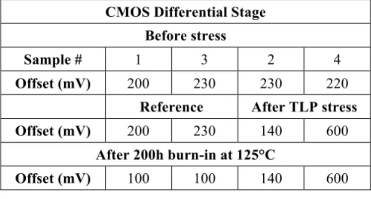
C. Differential stage circuit
In the same way, an analog circuit, namely a differential stage, was stressed between the power supply and ground using TLP testing. Step stressing was stopped when the IDDQ leakage current changed by a decade i.e. a few nanoamps, the initial current being in the 50 pA range. The TLP voltage level at which the leakage current started to increase is very low: it is seen from a TLP voltage as low as 10V. Offset measurement was used to monitor the impact on the reliability of the differential stage. The results are summarized in Table 3. In contrast to digital circuits, right after stress, there is a significant impact on the functionality of the circuit. It is either an
improvement of the offset (sample #2) or a serious degradation (sample #4). Hot-electron-induced input offset voltage degradation is a well-known phenomenon in CMOS differential stages [10-11]. During the ESD stress, that is probably the hot carrier injection into the oxide that induces such a rapid degradation even at very low TLP stress. Depending on which branch of the differential stage undergoes the hot carrier injection, it results in unbalanced branches (unbalanced threshold voltages) or on the contrary, more balanced ones. The samples also underwent a 200h burn-in experiment. In this case, the burn-in testing did not cure or degrade this characteristic.
Table 3: Comparator offset measurement before and after a TLP stress (leakage current~few nA) as well as after 125°C burn-in.
CMOS Differential Stage Before stress
Sample # 1 3 2 4
Offset (mV) 200 230 230 220
Reference After TLP stress
Offset (mV) 200 230 140 600
After 200h burn-in at 125°C
Offset (mV) 100 100 140 600
V. Latent defect detection
challenge
In our study, we have used IDDQ current measurements to characterize stressed devices. We have demonstrated that even a small current leakage results in a physical damage that did not modify the behavior of the ESD stressed device. On the other hand, we have shown that after a 200h burn-in, the leakage current related to this defect significantly evolves. No catastrophic failure was observed over this relatively short time but it can be assumed that the lifetime of the circuit is degraded.
The main question is therefore to know if this type of current measurement is appropriate for the detection of potential ESD induced latent defects into components dedicated to high reliability applications. This kind of approach is usually suitable for CMOS logic devices [12].
In steady state, a CMOS gate only dissipates a weak leakage current. For a defect-free CMOS gate, this leakage generally remains lower than a pA. At the transistor level, an ESD stress can induce physical defects such as gate oxide (gate-drain, gate-bulk or
gate source) or junction breakdown (drain-bulk, source-bulk).
ESD stresses can also induce other damages such as well-substrate junction breakdown or protection structure breakdown. The most usual result of these physical damages is a strong increase of the leakage current. Therefore, IDDQ testing for CMOS VLSI is an effective method to detect various physical defects such as shorts and bridging [13] induced by ESD. The detection of latent defects is a little bit more challenging since the leakage current can be very small. In the considered test circuits, the damaged structure is a PMOS transistor and the leakage current is only a few µA and it can be significantly less sometimes (nA range). But physical defects are already induced and can be located by thermal laser stimulation or by emission microscopy.
Table 4: Expected Ioff evolution for HP and LSP logic technologies.
Year 2001 2004 2007 2010
Technology node (nm) 130 90 65 45
HP Ioff (µA/µm) 0.01 0.1 1 3
LSP Ioff (pA/µm) 1 1 1 3
Detecting a defect-induced leakage current by electrical measurement has been done at the device level and we can consider two cases:
− ESD stress damages located at the I/O of the device (protection structure, input / output gates), − ESD stress damages inducing a “weak” structure
inside the die (core level).
In the first case, I(V) measurement remains very useful to detect ESD damages. We can track any discrepancy between the expected curve and the measured one as well as tracking curve modification after suspected ESD stress. In the second case, the key issue is to be able to determine the threshold level above which it can be stated that there is a latent defect at the transistor level (reverse biased junction or gate oxide). According to ITRS roadmap, the off current of MOS transistors is skyrocketing with the decrease of the transistor size and of the power supply. Table 4 [14] summarizes this relationship for High Performance (HP) and Low Standby Power (LSP) CMOS logic devices.
In HP VLSI, the quiescent power-supply current will rise up to hundreds of mA which makes defect induced current leakage detection very challenging. The effectiveness of conventional IDDQ testing in deep sub-micron is worn down. A lot of studies were
carried out to extend IDDQ testing capabilities. They are mostly based on statistical and differential IDDQ (DIDDQ) methods [15]. Unfortunately, the low current leakage values associated to latent defects appears to be undetectable even with this improved techniques for HP devices. It results that leakage current measurement are appropriate for the detection of weakly ESD stressed devices only for physical damages located at I/O structures or inside LSP devices. To overcome these limitations, we are currently studying the effect of ESD on low frequency noise level of stressed devices [16].
VI. Conclusion
The impact of CDM and TLP stresses on both digital and analog circuits was studied using a dedicated test circuit. Although digital circuits in this 0.6µm technology are quite robust and tolerant to ESD damages, the study shows that even at a low leakage current level (hundred of nA), a physical defect can be observed. For digital circuits and in agreement with other studies, such defects do not apparently change the functionality of the circuit. However, the defect evolves under burn-in or during storage inducing a significant increase of the IDDQ leakage current. The defect responsible for this leakage increase is melted filament across a reverse biased junction whereas a gate oxide breakdown does not impact the IDDQ current after burn-in. Analog circuits are more sensitive to ESD induced latent defects and can become out of specifications at low ESD stress level. For complex circuits, this study shows that IDDQ will not be able to detect an ESD induced defect in the range of 100nA to a few µA. Further investigations are currently carried out to assess the capabilities of low frequency noise measurements as a stress indicator in complex circuits. First results on a single device shows a much higher sensitivity than IDDQ measurement.
References
[1] Hugh Hyatt, ESD: Standards, Threats and System Hardness Fallacies, in EOS/ESD Symposium Proceedings, 2002, pp. 175-181.
[2] Space Operations Digest, The Aerospace Corporation, vol.1, n°1, Nov.20, 2002.
[3] H. A. Gieser, P. Egger, J.C. Reiner, M.R.
Herrmann, A CDM-Only reproducible field
degradation and its reliability aspect, in Quality and reliability engineering international, Vol. 10, 1994, pp. 341-350.
[4] V. Vassilev, G. Groeseneken, S. Jenei and al., Modeling and Extraction of RF Performance Parameters of CMOS Electrostatic Discharge Protection Devices, in EOS/ESD Symposium Proceedings, 2002, pp. 111-118.
[5] K. Nikawa and S. Tozaki, Novel OBIC Observation Method for Detecting Defects in Al Stripes Under Current Stressing, ISTFA 1993, pp. 303-310.
[6] E.I. Cole Jr., P. Tangyunyong, and D.L. Barton, Backside Localization of Open and Shorted IC Interconnections, IRPS 1998 Proceedings, pp.129-136.
[7] C. Boit, G. Shade, Photoemission
Microscopy, Microelectro,nic Failure Analysis Desk References, ISBN : 0-87170-638-5.
[8] B. Kaczer et al, Impact of MOSFET oxide breakdown on digital circuit operation and reliability, in IEDM’2000 Proceedings, San Francisco (USA), December 10-13, 2000, pp.553-556.
[9] B. Kaczer et al, Observation of hot-carrier-induced nFET gate-oxide breakdown in dynamically stressed CMOS circuits, IEDM’2002 Proceedings, San Francisco (USA), December 8-11, 2002, pp. 171-174.
[10] R. Thewes et al, Characterization and model of the hot-carrier-induced offset voltage of analog CMOS differential stages, IEDM’1994 Proceedings, pp. 303-306.
[11] S. Z. Mohamedi et al, Hot-electron-induced offset voltage degradation in CMOS differential amplifiers, IRPS’1992 Proceedings, pp. 76-80.
[12] A. W. Righter et al, CMOS Iddq reliability indicators and latent defect detection, ITC 1992 Proceedings, pp 194-203.
[13] R Rajsuman, Iddq Testing for CMOS VLSI, Proceedings of The IEEE, VOL.88, N°.4, pp. 544-566, April 2000.
[14] The International Technology Roadmap for Semiconductors: 2001, Process Integration chapter, Logic Technology Requirements Tables.
[15] C. Thibeault and L. Boisvert, Diagnosis Method Based on DIddq Probabilistic Signatures: Experimental Results, ITC 1998 Proceedings, pp 714-723.
[16] N. Guitard et al, Low Frequency Noise Measurements for ESD Latent Defect Detection in High Reliability Applications, ESREF’2004, Zurich (Switzerland), October 2004.