HAL Id: hal-03235158
https://hal.archives-ouvertes.fr/hal-03235158
Submitted on 25 May 2021HAL is a multi-disciplinary open access archive for the deposit and dissemination of sci-entific research documents, whether they are pub-lished or not. The documents may come from teaching and research institutions in France or abroad, or from public or private research centers.
L’archive ouverte pluridisciplinaire HAL, est destinée au dépôt et à la diffusion de documents scientifiques de niveau recherche, publiés ou non, émanant des établissements d’enseignement et de recherche français ou étrangers, des laboratoires publics ou privés.
optical modelling for quantum efficiency optimization
Chenxi Ma, Daming Zheng, Dominique Demaille, Bruno Gallas, Catherine
Schwob, Thierry Pauporté, Laurent Coolen
To cite this version:
Chenxi Ma, Daming Zheng, Dominique Demaille, Bruno Gallas, Catherine Schwob, et al.. Light management in highly-textured perovskite solar cells: From full-device ellipsometry characterization to optical modelling for quantum efficiency optimization. Solar Energy Materials and Solar Cells, Elsevier, 2021, 230, pp.111144. �10.1016/j.solmat.2021.111144�. �hal-03235158�
1
Light management in highly-textured perovskite solar cells: From full-device
ellipsometry characterization to optical modelling for quantum efficiency
optimization
Chenxi Ma1, Daming Zheng2, Dominique Demaille1, Bruno Gallas1, Catherine Schwob1, Thierry
Pauporté2 and Laurent Coolen1,*
1 Sorbonne Université, CNRS, Institut de NanoSciences de Paris, INSP, F-75005 Paris, France,
2 Chimie ParisTech, PSL Research University, CNRS, Institut de Recherche de Chimie Paris (IRCP),
UMR8247, 11 rue P. et M. Curie, F-75005 Paris, France. * Corresponding author : [email protected]
Abstract :
As perovskite solar cells (PSC) are now reaching high power conversion efficiencies, further performance improvement requires a fine management and harvesting optimization of light in the cells. These request an accurate understanding, characterization and modelling of the optical processes occurring within these complex, often textured, multi-layered systems. We consider here a typical methylammonium lead iodide (MAPI) solar cell built on a fluorine-doped tin oxide (FTO) electrode of high roughness. We used variable-angle spectroscopic ellipsometry (VASE) to design a one-dimensional (1D) optical model of the stacked layers describing the rough texture as layers of effective-medium index. While most previous reports on PSC optical models performed ellipsometry only on single layers of each material independently deposited on glass, our model was obtained by an extensive ellipsometric analysis of the full stratified PSC structure at each deposition step. We support the 1D model using data extracted from scanning electron microscopy, diffuse spectroscopy and photovoltaic efficiency measurements and compare its results with full 3D simulations. Although the 1D model is insufficient to describe scattering by the FTO plate alone, it gives an accurate description of the full device optical properties. By comparison with the experimental external quantum efficiency (EQE), we estimate the internal quantum efficiency (IQE) and the effect of the losses related to electron transfer. We finally discuss the optical losses mechanisms and possible strategies to improve light management and further increase PSC performances.
Introduction :
Hybrid organic-inorganic perovskite solar cells (PSC) have rapidly emerged as a promising candidate for efficient and cost-effective photovoltaic systems due to their strong light absorption, high charge carrier mobility and low processing costs.1 Recent developments of PSCs include the use
of interfacial self-assembled monolayers2 or two-dimensional (2D) layers,3 multiple cations
2 technology reaches a present record efficiency of 25.5%.6 Commercialization of single junction PSC or
in tandem with a silicon solar cell is under study by various industrial companies.7 As perovskite
materials now attain high performances and a rather good stability, further advances can be expected by optimizing light penetration in the devices and harvesting by the perovskite absorber.1,8-22 Accurate
optical models are necessary in order to explore such light management strategies, as well as to distinguish optical effects from charge separation and transfer effects in the overall experimental photovoltaic efficiency. Numerical finite-difference methods can be used to model a three-dimensional (3D) structure. However, if the structure can be described as a one-three-dimensional (1D) stack of planar layers, an exact analytical description can be obtained, with much shorter computation times, by the transfer-matrix method (TMM). Then, propagation through each layer and reflection at each interface are described by a 2x2 matrix, and the properties of the full stack are obtained simply as a product of these matrices.29 Numerous authors have used TMM to model PSCs18-23 as well as other
thin-film photovoltaic devices, as reviewed in ref. 28. The final target is to optimize the light management to further boost the cells performances. It requires a precise knowledge of the optical properties (complex index of refraction, thickness, roughness) of each layer of the device.
Ellipsometry is one of the best techniques for probing the optical properties of stacked thin films. It has been used in many experimental reports on PSC to determine the optical indices of each device material.17-27, 40 In silicon or organic photovoltaics, ellipsometric characterization of a full device
stacking has also been discussed in a perspective of monitoring industrial fabrication processes.28
However, data treatment and interpretation can become problematic for solar cells because stacks of many layers must be considered,29 so that performing ellipsometry on full solar cell devices, such as
thin-film cells for instance42-43, can be challenging. For this reason, reports on optical modelling of PSCs
usually use either literature indices or ellipsometry characteristics of the material obtained independently as a single layer on a standard substrate.13,18-23, 30 A much less abundant literature has
presented ellipsometry investigations on full PSC devices to validate the optical model,20,31,44-45 even
though materials deposition is known to depend critically on the substrate.
Modelling the device as a stack of independently-characterized layers is all the more difficult and possibly inappropriate in the presence of rough interfaces. The layer of transparent conducting oxide employed as the front contact can present a rough texture16-18,28,32 of up to hundreds of
nanometers in height30 with possible effects on the device’s efficiency.8 Some deposition protocols for
the perovskite and other layers can also generate a significant roughness.9, 13, 33 Rough interfaces affect
solar cell optical properties and intentional texturing can be a tool for light management because (i) it creates an effective index gradient which facilitates light penetration into the active absorber layer and (ii) it scatters light to higher internal propagation angles so that it remains trapped within the device and is better absorbed.1, 8-12, 34 Index-gradient effects can be probed by ellipsometry, from which a
one-dimensional (1D) model of stacked planar layers can be derived and treated by the transfer-matrix method (TMM). Rough interfaces are then treated by introducing intermediate planar layers of mixed composition described by an effective medium approximation (EMA).29 On the other hand, light
scattering cannot be quantified by specular ellipsometry nor described by a 1D model of planar layers. Diffuse spectroscopic methods and 3D simulations must then be used to provide a more realistic physical model and assess the limitations of the 1D model.
It is thus necessary to establish accurate ellipsometry protocols for the full PSC devices characterizations, particularly in the case of highly textured interfaces, and to assess the validity of the derived optical 1D models by in-depth comparison with other available experimental data and 3D
3 simulations. In this paper, we investigate a typical PSC structure built on a front electrode with a very rough surface. We characterize the device by ellipsometry at each step of the deposition, leading to a model of the structure as a 1D stack of planar layers, with EMA layers describing textured interfaces. We then analyze the validity of this 1D model as compared to 3D numerical simulations by confronting them with other experimental data obtained by electron and atomic-force microscopy, direct and diffuse transmission spectroscopy. From the device’s optical behavior determined theoretically, we have then been able to determine the theoretical light harvesting efficiency spectrum that we have compared with the experimental external quantum efficiency (EQE) of the cell. Based on this analysis, we finally discuss some potential light-management improvement paths.
Results and discussion :
For this analysis, we chose the typical perovskite solar cell stacking presented in Fig. 1(a). The cells, fully detailed in Ref. [35], were based on methyl ammonium lead iodide (CH3NH3PbI3, MAPI) and
reached a power conversion efficiency up to 19%. A SnO2:F (fluorine-doped tin oxide - FTO) layer was
used as the front contact electrode36. These commercial substrates (TEC7, Pilkington - hereafter named
"FTO plate") are made of a soda-lime glass slide, covered by a thin SnO2 layer, a thin SiO2 layer, and
the FTO layer.18,28 The role of the two oxide sub-layers is to avoid color effects due to interferences.28
A compact TiO2 layer was deposited by spray-pyrolysis on top of the FTO as the electron transporting
layer (ETL), followed by a mesoporous TiO2 layer (30-nm TiO2 nanospheres) in order to maximize the
charge collection and transfer to the ETL. The active MAPI layer was then spin-coated as described in ref. 37 : Figure 1(c) shows a SEM image of the sample cross-section at this stage. It was then covered by a layer of 2,2’,7,7’-tetrakis(N,N’-di-p-methoxyphenylamine)-9,9’-spirobifluorene (Spiro-OMeTAD) which acts as the hole transporting layer (HTL) and by a gold film acting as the back-contact electrode.
Figure 1 : (a) Scheme of the solar cell structure. (b) Atomic-force microscopy (AFM) image of the surface of the fluoride-doped tin oxide (FTO) layer. (c) Scanning electron microscopy (SEM) cross-sectional view of the sample after methyl ammonium lead iodide (MAPI) deposition (before Spiro-OMeTAD and gold deposition ; the colors are added as a guide for the eye).
4 FTO is the most popular transparent conducting oxide employed in PSCs.28 As compared to
indium tin oxide (ITO), it offers lower costs and a better stability and resistance to high temperatures. However, many manufactured FTO samples are known to present high surface roughness (RMS).8, 17, 28, 30 From AFM images of the FTO surface (fig. 1(b)), we found in our case a root-mean-square
roughness of 43 nm. The scanning electron microscopy (SEM) profile (fig. 1(c)) also shows clearly the FTO texture, with peak-to-peak heights as large as 100-200 nm. In spite of the large FTO roughness, the two TiO2 layers, compact and mesoporous, were well-covering and followed almost perfectly the
underlying FTO texture profile. As a result, the roughness of these layers, measured by atomic-force microscopy (AFM) at 39 and 27 nm, respectively, were close to the roughness of the FTO surface. On the other hand, the MAPI layer was much thicker and smoothed the surface (Fig. 1(c)).
Ellipsometry relies on measuring the ratio of the p-polarized to s-polarized reflection spectra and fitting them with a one-dimensional (1D) model of planar layers. The fitting parameters are thus the complex index of refraction and thickness of each layer. The roughness of an interface between two materials is described in the model by adding one or several layers containing a mixture of the two materials. The complex index of the mixture was described here within a Bruggeman-type effective medium approximation (EMA) and the fitting parameters were the EMA layer thickness and the composition of the mixture. When considering a stack of numerous layers, including some large roughness, many variables must thus be adjusted to fit the experimental data and it is necessary to support the resulting optical model by as much experimental data as possible.29 In this study, we
performed variable-angle spectroscopic ellipsometry (VASE) at three different incidence angles, and at each step of the device deposition. Moreover, preliminary estimates for the indices of the materials were either determined independently by depositing each material individually on a glass substrate and performing an ellipsometric characterization, or were found in literature tables for the most standard materials (see Supporting information – S.I. - for the protocol and resulting real and imaginary index curves). All optical constants extracted from ellipsometry were found in excellent agreement with literature data, as discussed in S.I. sections A and E. The mesoporous TiO2 layer was well-described
by an EMA layer of air and TiO2, as expected since the TiO2 spheres were much smaller (~30 nm
diameter) than the optical wavelength.
Figure 2 displays the measured ellipsometric data (full lines) for the FTO commercial substrate (Fig. 2(a)), for each new deposited layer (Figs. 2(b) to (e)) and for the full device (Fig. 2(f)). At each step (a) to (f), a 1D optical model of the system was established (right column of fig. 2) yielding theoretical curves (dotted lines) which were all in very good fit agreement with the experimental spectra (fit parameter details in S.I. section D). The FTO-TiO2-MAPI portion is quite complex since the amplitude
of the FTO texture is larger than the thickness of the two upper TiO2 layers. Therefore a ternary mixture
of FTO, TiO2 and MAPI had to be considered, and three successive EMA layers were used. No
adjustment of the pre-determined indices was necessary in order to optimize the model agreement with the data. The only free parameters were the thickness of each layer and the composition of the three EMA mixtures. At each new deposition step, unless stated otherwise in the figure, a good fit could be obtained while keeping the same model for the underlayers and just replacing air by the newly-deposited material and adding more layers on top. From Fig. 2(e) to (f), a significant change of the Spiro-OMeTAD thickness had to be introduced, from 192 to 228 nm, but Figure 2(f) is dominated by the Au absorption so that the Spiro-OMeTAD thickness might be less precise than the value from Fig. 2(e). The thicknesses obtained from ellipsometry well-match those estimated from the SEM image
5 of Fig. 1(c). The index profile within the stack of three EMA layers is in acceptable agreement with the index profile calculated by averaging over the 3D structure as known from the SEM image (see detailed discussion in section B of the Supporting information). Apart from this portion, no other EMA layer needed to be introduced to describe the roughness of the other interfaces.
Figure 2 : Left and middle columns : measured (full lines) and fitted (dotted lines) ellipsometric curves at each successive step of sample deposition, at incidence angles 50° (blue), 60° (green) and 70° (red). Right column : model structure obtained by fitting the ellipsometric data (EMA layers are represented by hatches). This structure will define the 1D model used in the following of the paper.
6 Although ellipsometry data are consistent with the 1D model at each step of the device deposition, some other optical properties are absolutely not well-described by this model. In particular, Fig. 3(a) compares the measured total transmission spectrum of the FTO plate with the spectrum calculated according to the 1D model of this FTO plate (shown in Fig. 2(a)). The two curves differ significantly over the whole visible range, in particular at blue wavelengths. Scattering by the rough sample surface is the likely explanation for this difference, as it is anticipated to decrease the transmitted intensity and have a stronger effect at lower wavelengths (wavelengths which are comparable to the 100-200 nm scale of the roughness patterns). This is confirmed by measuring the diffuse transmission spectrum with an integrating sphere (Fig. 3(b)). A significant fraction of the total light incident intensity is scattered by the FTO layer: up to 20 % at 350 nm. While the effective index gradient induced by the roughness can be well-probed by ellipsometry, as demonstrated in Fig. 2, scattering is not well-analyzed because ellipsometry relies on the ratio between s- and p-polarizations so that it is little affected by reflection losses due to scattering (as long as they have low polarization dependence).
Figure 3 : (a) Direct transmission spectrum of the fluoride-doped (FTO) substrate : experimental (full line) and simulated within the 1D model of fig. 2(a) (dotted line). (b) Direct (blue) and diffuse (green) transmission spectra of the FTO substrate at normal incidence. (c) Schematic of the full-stack 3D model structure for the finite-elements simulation. The FTO upper surface has a random profile of root-mean-square (RMS) roughness 50 nm. (d) Transmission curves of the FTO plate (top) and the FTO plate covered by a compact TiO2 layer (bottom) :
experimental (blue line), calculated from the 1D model described in figs. 2(a) and (b) (yellow dotted line), modelled by the 3D finite-element calculation with a rough surface (green line).
Since a 1D model, by definition, can only describe direct transmission and reflection, it is necessary to build a numerical 3D model of the sample in order to well-describe scattering effects. We designed our 3D model as depicted in Fig. 3(c) for the full device ; for the FTO plate alone and for the intermediate deposition steps, the same model was used with the upper layers replaced by air. We
7 considered for all materials the same thicknesses and indices as determined by ellipsometry (Fig. 2(f)). Mesoporous TiO2 was described as an EMA layer, like for the 1D model : we will not discuss effects of
scattering by the TiO2 spheres as their mean diameter is much smaller than any wavelength
considered. A random surface texture was introduced for the FTO plate with 50-nm RMS roughness. For the compact and mesoporous TiO2 layers, their texture was a translation of the FTO layer texture
(see the structure profile in Fig. 5c), with a reduced RMS roughness (30 nm) for the mesoporous layer in order to take into account its lower roughness measured by AFM. The thickness of the compact and mesoporous TiO2 layers cannot be extracted from the ellipsometric data, where they are hidden inside
EMA layers. We used the thicknesses determined for compact and mesoporous TiO2 deposited
independently on glass (respectively 43 and 166 nm – see S.I. section A).
Figure 3d plots the experimental transmission spectra of the FTO plate (top) and of the FTO plate covered by the compact TiO2 layer (bottom), superimposed with the results of the 1D model and
of the 3D model. For both samples, the 1D model overestimates the actual transmission, especially in the visible range, because it does not take into account scattering losses. The 3D model, on the other hand, describes the experimental data with an excellent precision. For the FTO plate, the agreement is better than 1.5 % above 400 nm. For the FTO+TiO2 sample, it is slightly less good due to the increased
sample complexity but remains better than 4.5 % (standard deviation 2 %). The 3D model thus provides an excellent modelling of the experimental structures, even when the roughness causes a strong scattering, while the 1D model is not able to describe scattering effects in the transmission spectra.
8
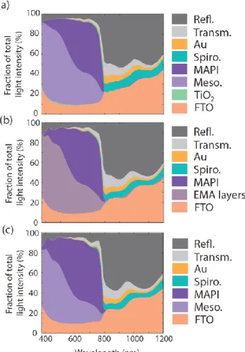
Figure 4 : Theoretical fractions of light absorbed by each layer of the solar cell and reflected or transmitted by the device, obtained (a) from the 3D model of roughness (as described in fig. 3(c)), (b) from the 1D model of roughness (as described in fig. 2(f)), (c) without including any roughness (planar FTO-TiO2-mesoporous TiO2-MAPI
interfaces). Absorption by the compact TiO2 layer is negligible in (b) and (c). For simplicity under “FTO” are
included all layers of the FTO plate : SnO2, SiO2 and SnO2:F.
The relevant optical information for PSC devices is the ratio between perovskite absorption, which generates the charges, on the one hand, and transmission and reflection of the device and parasitic absorption by the other layers, on the other hand. While transmission and reflection can be probed experimentally, the absorption of each layer can only be accessed through simulations. Figure 4 compares the results of the 3D model (Fig. 4a) and of the ellipsometric 1D model (Fig. 4b). Note that in the 3D model the active layers are the MAPI layer and the mesoporous layer (which contains MAPI and TiO2 but TiO2 absorption is negligible above 400 nm). On the other hand, in the 1D model, the
active layers are the MAPI layer and the three EMA layers but only part of the latter absorption is active for charge generation since it includes also FTO absorption. Within both models, absorption by the active layers dominates the visible spectrum. The first 150-200 nanometers of the active medium (corresponding to the mesoporous layer in the 3D model and the EMA roughness layers in the 1D model) contribute to most of the absorption in the blue range and of a significant portion in the red range. This can be explained by the strong MAPI absorption: as shown in the electric field distribution (Fig. S4), most of the incoming beam is absorbed already by MAPI in the mesoporous region and does not reach the MAPI capping layer. We have also noted that the absorbance of the mesoporous layer follows the absorbance curve of MAPI (Fig. S5). MAPI absorption is especially strong at lower wavelengths due to the higher imaginary index component.18-19, 24, 30 Parasitic absorption is caused
essentially by FTO, as calculated previously on similar systems,18 while the front electrode (air-glass
interface) causes around 4 % reflection.
The plots of Figs. 4a and 4b are in excellent agreement, with only a few fringes added in fig. 4b to the reflection component because of interferences in the 1D model (which are not present in the 3D model because of the rough interfaces). This shows that the 1D model obtained from our spectroscopic ellipsometry protocol provides an accurate description of the absorption of the various layers of the full PSC structure. As compared to the case of the FTO plate alone (fig. 3), the full device is probably less affected by scattering because in the FTO plate the index contrast at the FTO/air interface is very high, while in the device the index contrast between FTO, TiO2 and MAPI is much
lower. We also plot in Fig. 4c the result of a 1D structure where no FTO roughness is included (only planar FTO-TiO2-mesoporous TiO2-MAPI layers). The optical behavior of the planar structure is very
similar to the rough sample. This indicates that, even though the sample roughness creates an effective gradient index which might modify the optical properties, this effect is quite low, again because of the low index contrast between FTO, TiO2 and MAPI. Eventually, the similarities between figs. 4a, b, and c
show that the large roughness of the FTO surface has no significant effect on the full-PSC optical properties, so that a rough FTO plate can be used as well as a smoother one as far as optical properties are concerned.
Finally, the percentage of incident light which is absorbed by the active layers constitutes the light-harvesting efficiency (LHE) and can be calculated from the simulated data of Fig. 4. Fig. 5a plots the LHE spectral dependence for the two (1D and 3D) models with roughness, along with the case without roughness. As expected, given the similarities of Figs 4(a) to (c), the three curves are very close. We compare these curves with the experimental external quantum efficiency (EQE) (ratio of the number of collected charges to the number of incident photons) averaged over four solar cells
9 obtained by the same highly-reproducible35 deposition process as before. The LHE and EQE curves are
in overall qualitative agreement, with ±10 % differences discussed below. The slight oscillation features at 410 nm and 500 nm of the experimental EQE curve are well reproduced by the 1D model, but not by the 3D model, suggesting that the latter model might overestimate scattering effects leading to reduced interference fringes.
The internal quantum efficiency (IQE), percentage of absorbed photon leading to electron collection, is equal to the ratio EQE/LHE and reflects losses in the charge transfer and collection processes. In figure 5(b) we plot an estimate of the IQE by dividing the experimental EQE by the theoretical LHE. Given the very complex optical nature of this stratified medium, it is satisfying to find that the IQE spectral dependence is, as expected, completely distinct from the spectral dependence of the device’s optical properties contained in the LHE. This was not the case in previous reports on PSC modelling,18, 30 which may illustrate the need for a precise full-device characterization in order to
estimate the LHE accurately. However, the IQE values below 550 nm are slightly (1-1.1) above unity, which is unphysical because each absorbed photon cannot lead to more than one electron collection. This may be attributed most likely to EQE measurement differences between PSC samples (fig. S11) or perhaps to a slightly underestimated theoretical LHE, if MAPI absorption is higher or FTO absorption is lower than measured from ellipsometry or if the role of scattering in enhancing absorption is not fully described even by the 3D model. Note however that most MAPI complex indices from the literature are not significantly different from ours (fig. S7) and would yield very similar LHE curves (fig. S8). Our deposition protocol has been shown to provide highly-stable MAPI layers35 so that effects of MAPI
degradation can also be excluded. Moreover, MAPI degradation into PbI2 would induce sub-bandgap
absorption above 800 nm41 which is absent in our ellipsometric data. Slight differences between the
layer thicknesses in the ellipsometry sample and the EQE sample would also have a weak effect on the LHE (figs. S9 and S10).
The IQE exhibits a continuous decrease from 350 to 700 nm, probably because absorption in the red range occurs deeper in the MAPI layer (because MAPI absorbs less at these wavelengths), further from the mesoporous TiO2 layer, so that electron transfer to the TiO2 ETL is less efficient. We
thus estimate the charge transfer losses, in the red spectral domain, to 5-15 %. On figure 5(d), we evaluate theoretically the average perovskite absorption position within the device, defined as 〈𝑧𝑃𝑎𝑏𝑠(𝑥, 𝑦, 𝑧)〉/〈𝑃𝑎𝑏𝑠(𝑥, 𝑦, 𝑧)〉 where the average is performed over the active layers. At shorter wavelengths, the absorption is located very close to the planar TiO2 layer, so that the IQE is highest
and probably close to unity. Light absorption then shifts deeper into the mesoporous TiO2 layer and
10
Figure 5 : (a) Experimental External Quantum Efficiency (EQE ; blue dots) and theoretical Light Harvesting Efficiency (LHE) curves calculated from the 3D model (green) and the 1D model with (red) and without roughness (blue line). The LHE is the fraction of incident light absorbed by the active material. (b) Estimate of the internal quantum efficiency obtained by dividing the experimental EQE by the theoretical LHE (from the 3D model) (IQE calculated from 370 to 800 nm as above 800 nm the EQE and LHE are almost zero). (c) Real index profile of the 3D model at 551 nm. (d) Theoretical light absorption position within the sample (from the 3D model), defined as
〈𝑧𝑃𝑎𝑏𝑠(𝑥, 𝑦, 𝑧)〉/〈𝑃𝑎𝑏𝑠(𝑥, 𝑦, 𝑧)〉, as a function of wavelength.
Eventually, this work suggests several paths for light management improvement in such PSCs. (i) Over the MAPI absorption spectral range, a first limitation to the LHE is the reflection (around 4 %) of the incoming beam at the air-glass interface. This is a fundamental limit for a planar surface but it can be overcome by texturing the surface, as it is already done in commercial silicon devices. For instance, a textured light-management foil added by nanoimprint lithography on the glass surface of a PSC has shown 5 % relative improvement of the cell performance.38 (ii) A second optical limitation is
absorption by the front electrode layers of SnO2 and SnO2:F. A thinner electrode may be used, provided
that the charge conduction remains adequate. Indium-tin oxide (ITO) electrodes also seem a good alternative as lower evaluations of their parasitic absorption have been reported.13, 19 (iii) A third, less
important, optical loss mechanism is transmission through the gold electrode : it is negligible at 400 nm but increases up to 3 % at 700 nm and 9 % at 780 nm. A first way to avoid such losses would be to increase the MAPI layer’s thickness, however at the risk of degrading the perovskite crystalline
11 structure and reducing the charge transfer efficiency. A better alternative is to increase the thickness of the back-reflecting gold electrode. We model that an increase from 26 to 50 nm would reduce the device transmission in the visible range by a factor around 6, without any significant change in the gold and HTL absorption. Absorption by the active layer could then increase by an absolute 2 % at 700 nm, 3 % at 750 nm and 4 % at 780 nm. (iv) Parasitic absorption by the other materials (gold, spiro-OMeTAD, TiO2) is negligible so that no improvement can be obtained from modifying these layers. (v) In terms
of charge transfer within the device, the IQE decrease as a function of the wavelength can be attributed to charge generation deeper in the MAPI layer at higher wavelengths. This shows that the hole transfer undergoes minor losses while significant losses occur during electron transfer to TiO2 (around 10-20 %
at 700 nm). Increasing the thickness of the mesoporous TiO2 layer could favor electron transfer without
introducing optical losses.
Conclusion :
We have analyzed the effects of large substrate roughness (43 nm RMS) on the optical properties of a typical perovskite solar cell. We showed that ellipsometry is an effective technique for the complete characterization of PSC full layers stack. It provides a precise characterization in spite of the extreme complexity of the system. We tested the predictions of the resulting 1D model and found that, while a 3D model was necessary to describe the optical properties of the FTO plate alone, the full device could be described by the ellipsometric 1D model with little difference compared to the 3D model. Roughness effects within the full PSC device were shown to be quite limited, due to the low index contrast at the rough interfaces. We measured the PSC external quantum efficiency and found a good agreement of its spectral dependence with the calculated light-harvesting efficiency. This allowed us to probe the changes of the internal quantum efficiency over the absorption range and quantify the effect of the light penetration depth within the active layer on the electron transfer efficiency. Finally, we used the optical model to list the possible light-management strategies to improve the device.
Methods :
Fabrication : The FTO glass (TEC7, Pilkington) was purchased from Nippon Sheet Glass Co. Ltd. The compact TiO2
layer was fabricated by spray pyrolysis method. The precursor solution of 7 mL isopropanol, 0.6 mL titanium isopropoxide, and 0.4 mL acetylacetone was sprayed onto substrates placed on a hot plate by a pressurized air gas gun and preheated at 455°C, 20 min before spray.35,36
The mesoporous TiO2 layer was deposited by spin coating.37 The TiO2 paste (30-nm diameter spheres) was diluted
in ethanol in a 1:7 mass ratio, dispersed by ultrasonic wave, then stirred for 12 h in brown bottles to avoid light. This solution was spin-coated at 4000 rpm (2000 rpm/s acceleration) for 20 s then dried at 70°C for 10 min. Afterward, the samples were annealed at 500°C for 30 min then let to cool down to around 200°C.
The perovskite layer was deposited by a one-step method based on the spin coating technique in a dry box.35
The CH3NH3PbI3 (MAPI) precursor solution consisted of 334 mg PbI2, 115 mg methylammonium iodide (MAI),
dissolved in 500 μL dimethyl sulfoxide (DMSO: (CH3)2SO) .This precursor was spin-coated in two steps (1) at 1000
12
anti-solvent of 100 μL was dropped 10 s before the end of the spin coating program to trigger the fast-crystallization of the perovskite material. The samples were then annealed at 105°C for 1 h.
The Spiro-OMeTAD layer was prepared by spin-coating as described in a previous work by some of us.36 The
solution was prepared by dissolving 72 mg Spiro-OMeTAD in 1 ml chlorobenzene. Then, 17.5 μL bis(trifluoromethylsulfonyl)imide lithium salt (LiTFSI) solution (520 mg in 1 mL acetonitrile (ACN)), 28 μL
tert-butylpyridine (TBP) and 6 μL
tris((2-1H-pyrazol-1-yl)-4-tert-butylpyridine)-cobalt(III)-tris(bis(trifluoromethylsulfonyl)imide) (300 mg in 1 mL of ACN) were added into this solution, 35 μL of which was spin-coated at 4000 rpm (2000 rpm/s acceleration) for 30 s.36
Finally, a thin layer of gold was thermally evaporated through a mask to act as an electrode and back reflecting mirror.
Ellipsometric characterization : Ellipsometric measurements were performed by a V-VASE ellipsometer from J.A.
Woollam Co., Inc. A translucent tape was applied to the bottom of the sample to eliminate back reflection, which might interfere with the surface reflection, and a back reflection correction parameter was introduced. The scanning wavelength range was from 300 to 2000 nm in steps of 10 nm and incidence angles of 50°/60°/70°. The complex reflectance ratio ρ is defined as ρ =𝑟𝑝
𝑟𝑠 = tan Ψ ∙ 𝑒
𝑖∆, where tan Ψ is the amplitude ratio and Δ is the
phase difference between the two p and s polarizations. Then the software WVASE32 was utilized to fit a model of stacked layers of appropriate optical constants and thicknesses to the experimental curves Ψ(𝜆) and Δ(𝜆). The ellipsometric measurements were performed on the samples within a few hours from their deposition and lasted two hours. The rest of the time, the samples containing MAPI were stored in a N2-filled glovebox and
protected from light by aluminum foil.
Transmission spectra : Transmission spectroscopy was carried out by Cary 5000 UV-Vis-NIR spectrophotometer.
Our measurement range of wavelength was from 300 nm to 2000 nm with a spectral resolution of 1 nm.
External quantum efficiency : The EQE spectra were measured with an Oriel Instruments QuantX-300 system.46 3D simulations : The simulations were performed using the FDTD method with Lumerical software. We defined
a 3D-computing cell (1.5µmx1.5µm in x and y the dimensions of the layers and 8.5µm in z, the dimension of the stack) with periodic conditions in x and y and phase-matching layers to avoid parasitic reflections in z.
The stack (z= -0.5 µm to z= 0.9µm), deposited on a 6-µm microscope glass slide (from z= -6.5µm to z= -0.5µm), was illuminated by a plane wave at normal incidence, located at z= -5.5µm (inside the glass slide to avoid interference fringes due to the air/glass and stack/air interfaces). The transmission and reflection spectra were corrected by the transmission of the air/glass interface to be compared to the experimental ones.
The light source had a spectral range from 370 to 2000 nm for transmission and reflection simulations (resolution: 8.15 nm) and from 450 to 1200 nm for absorption simulations (resolution : 7.5 nm). For reflection and transmission simulations, we recorded the transmitted power, normalized by the source incident power, on two planes located at z= -6.5µm for reflection and z= 1.8µm for transmission.
For absorption simulations, we used a 3D-detector to record the electric field amplitude and the real and imaginary parts of the optical index at different points (x, y z) for 100 values of the wavelength (from 450 to 1200 nm). The resolution was 20 nm in x and y and 6.5 nm in z.
The roughness of the FTO and TiO2 layers were simulated using the random surface tool of Lumerical. The
roughness is generated by creating a random matrix of values in k space defined by the spans in x and y. A Gaussian filter is applied to this matrix, then a Fourier transform is used to transform the matrix back to real
space. The roughness used was characterized by an RMS amplitude of 50 nm (for the FTO and TiO2 compact
layers) and of 30 nm (for the TiO2 mesoporous layer) and by a correlation length of 100 nm in x and y. All our material indices are made available online.
13 Mr D. Z. acknowledges the CSC-Paristech program for scholarship funding (grant number 201806310126). Prof. T. P. acknowledges the Agence Nationale de la Recheche (ANR) for financial support via the Moreless project ANR-18-CE05-0026.
The authors would like to thank Christine Andraud (MNHN, Paris) for her advice on analyzing diffuse reflection.
Conflicts of interest
There are no conflicts to declare.
References
[1] Mauricio E. Calvo, Materials chemistry approaches to the control of the optical features of perovskite solar cells, J. Mater. Chem. A 5, 20561 (2017) ; Eui Hyuk Jung, Nam Joong Jeon, Eun Young Park, Chan Su Moon, Tae Joo Shin, Tae-Youl Yang, Jun Hong Noh and Jangwon Seo, Efficient, stable and scalable perovskite solar cells using poly(3-hexylthiophene), Nature 567, 511 (2019),
[2] T. Zhu, J. Su, F. Labat, I. Ciofini and Th. Pauporté, Interfacial Engineering through Chloride-Functionalized Self-Assembled Monolayer for High Efficiency Perovskite Solar Cells. ACS Appl. Mater Interfaces 12, 744 (2020) ;
Amran Al-Ashouri, Artiom Magomedov, Marcel Roß, Marko Jošt, Martynas Talaikis,Ganna Chistiakova, Tobias
Bertram,José A. Márquez, Eike Köhnen, Ernestas Kasparavičius,Sergiu Levcenco, Lidón Gil-Escrig,Charles J.
Hages,Rutger Schlatmann, Bernd Rech,Tadas Malinauskas,Thomas Unold, Christian A. Kaufmann, Lars Korte,
Gediminas Niaura, Vytautas Getautis and Steve Albrecht, Conformal monolayer contacts with loss-less interfaces for perovskite single junction and monolithic tandem solar cells, Energy Environ. Sci. 12, 3356 (2019), [3] T. Zhu, D. Zheng, J. Liu, L. Coolen and Th. Pauporté, Electrical Response of High Efficiency and Stable Solar Cells Based on MACl Mediated Grown FA0.94MA0.06PbI3 Perovskite. ACS Appl. Mater. Interfaces 12, 37197−37207
(2020) ; Qi Jiang, Yang Zhao, Xingwang Zhang, Xiaolei Yang, Yong Chen, Zema Chu, Qiufeng Ye, Xingxing Li, Zhigang Yin and Jingbi You, Nature Photonics 13, 460 (2019),
[4] P. Wang, M. Ulfa, T. Pauporté, Effects of Perovskite Monovalent Cation Composition on the High and Low Frequency Impedance Response of Efficient Solar Cells. J. Phys. Chem. C 122, 1973 (2018) ; Yinghong Hu, Eline M. Hutter, Philipp Rieder, Irene Grill, Jonas Hanisch, Meltem F. Aygüler, Alexander G. Hufnagel, Matthias Handloser, Thomas Bein, Achim Hartschuh, Kristofer Tvingstedt, Vladimir Dyakonov, Andreas Baumann, Tom J. Savenije, Michiel L. Petrus and Pablo Docampo, Understanding the Role of Cesium and Rubidium Additives in Perovskite Solar Cells: Trap States, Charge Transport and Recombination, Advanced Energy Materials 8, 1703057 (2018),
[5] T. Zhu, D. Zheng, M.-N. Rager and Th. Pauporté, Actual Organic Cations Composition Determination in Perovskite Thin Films. Application to Formamidinium Lead Iodide Stabilization for High Efficiency Solar Cell. Sol. RRL 2000348 (2020) ; M. Kim, G.-H. Kim, T. K. Lee, I. W. Choi, H. W. Choi, Y. Jo, Y. J. Yoon, J. W. Kim, J. Lee, D. Huh, H. Lee, S. K. Kwak, J. Y. Kim and D. S. Kim, Methylammonium chloride induces intermediate phase stabilization for efficient perovskite solar cells, Joule 3, 1 (2019),
[6] NREL Best Research-Cell Efficiency Chart (October 2020), https://www.nrel.gov/pv/cell-efficiency.html [7] Andy Extance, Perovskites on trial, Nature 570, 429 (2019),
[8] Biao Shi, Bofei Liu, Jingshan Luo, Yuelong Li, Cuicui Zheng, Xin Yao, Lin Fan, Junhui Liang, Yi Ding, Changchun Wei, Dekun Zhang, Ying Zhao and Xiaodan Zhang, Enhanced light absorption of thin perovskite solar cells using textured substrates, Solar Energy Materials and Solar Cells 168, 214 (2017),
14
[9] Lingling Zheng, Yingzhuang Ma, Saisai Chu, Shufeng Wang, Bo Qu, Lixin Xiao, Zhijian Chen, Qihuang Gong, Zhaoxin Wu and Xun Hou, Improved light absorption and charge transport for perovskite solar cells with rough interfaces by sequential deposition, Nanoscale 6, 8171 (2014),
[10] Alexander R. Pascoe, Steffen Meyer, Wenchao Huang, Wei Li, Iacopo Benesperi, Noel W. Duffy, Leone Spiccia, Udo Bach and Yi-Bing Cheng, Enhancing the optoelectronic performance of perovskite solar cells via a textured CH3NH3PbI3 morphology, Adv. Funct. Mater. 26, 1278 (2016),
[11] Mingzhu Long, Zefeng Chen, Tiankai Zhang, Yubin Xiao, Xiaoliang Zeng, Jian Chen, Keyou Yan and Jianbin Xi, Ultrathin efficient perovskite solar cells employing a periodic structure of a composite hole conductor for elevated plasmonic light harvesting and hole collection, Nanoscale 8, 6290 (2016),
[12] Mohammad Mahdi Tavakoli, Qingfeng Lin, Siu-Fung Leung, Ga Ching Lui, Hao Lu, Liang Li, Bin Xiang and Zhiyong Fan, Efficient, flexible and mechanically robust perovskite solar cells on inverted nanocone plastic substrates, Nanoscale 8, 4276 (2016),
[13] Salman Manzoor, Jakob Häusele, Kevin A. Bush, Axel F. Palmstrom, Joe Carpenter III, Zhengshan J. Yu, Stacey F. Bent, Michael D. McGehee and Zachary C. Holman, Optical modeling of wide-bandgap perovskite and perovskite/silicon tandem solar cells using complex refractive indices for arbitrary-bandgap perovskite absorbers, Opt. Express 26, 27441 (2018),
[14] Daniel A. Jacobs, Malte Langenhorst, Florent Sahli, Bryce S. Richards, Thomas P. White, Christophe Ballif, Kylie R. Catchpole and Ulrich W. Paetzold, Light management : a key concept in high-efficiency perovskite/silicon tandem photovoltaics, J. Phys. Chem. Lett. 10, 3159 (2019),
[15] Qiaojing Xu, Ying Zhao and Xiaodan Zhang, Light management in monolithic perovskite/silicon tandem solar cells, Sol. RRL 1900206 (2019),
[16] Juan-Pablo Correa-Baena, Miguel Anaya, Gabriel Lozano, Wolfgang Tress, Konrad Domanski, Michael Saliba, Taisuke Matsui, Tor Jesper Jacobsson, Mauricio E. Calvo, Antonio Abate, Michael Grätzel, Hernan Miguez and Anders Hagfeldt, Unbroken perovskite : interplay of morphology, electro-optical properties, and ionic movement, Adv. Mater. 28, 5031 (2016),
[17] Mohd Sharizal Alias, Ibrahim Dursun, Makhsud I. Saidaminov, Elhadj Marwane Diallo, Pawan Mishra, Tien Khee Ng, Osman M. Bakr and Boon S. Ooi, Optical constants of CH3NH3PbBr3 perovskite thin films measured by
spectroscopic ellipsometry, Opt. Express 24, 16586 (2016),
[18] James M. Ball, Samuel D. Stranks, Maximilian T. Hörantner, Sven Hüttner, Wei Zhang, Edward J. W. Crossland, Ivan Ramirez, Moritz Riede, Michael B. Johnston, Richard H. Friend and Henry J. Snaith, Optical properties and limiting photocurrent of thin-film perovskite solar cells, Energy Environ. Sci. 8, 602 (2015),
[19] Maarten van Eerden, Manoj Jaysankar, Afshin Hadipour, Tamara Merckx, John J. Schermer, Tom Aernouts, Jef Poortmans and Ulrich W. Paetzold, Optical analysis of planar multicrystalline perovskite solar cells, Adv. Optical Mater. 5, 1700151 (2017),
[20] Chang-Wen Chen, Sheng-Yi Hsiao, Chien-Yu Chen, Hao-Wei Kang, Zheng-Yu Huang and Hao-Wu Lin, Optical properties of organometal halide perovskite thin films and general device structure design rules for perovskite single and tandem solar cells, J. Mater. Chem. A 3, 9152 (2015),
[21] Jérémie Werner, Gizem Nogay, Florent Sahli, Terry Chien-Jen Yang, Matthias Bräuninger, Gabriel Christmann, Arnaud Walter, Brett A. Kamino, Peter Fiala, Philipp Löper, Sylvain Nicolay, Quentin Jeangros, Bjoern Niesen and Christophe Ballif, Complex refractive indices of Cesium-formamidinium-based mixed-halide perovskites with optical band gaps from 1.5 to 1.8 eV, ACS Energy Lett. 3, 742 (2018),
[22] Laurie J. Phillips, Atef M. Rashed, Robert E. Treharne, James Kay, Peter Yates, Ivona Z. Mitrovic, Ayendra Weerakkody, Steve Hall and Ken Durose, Maximizing the optical performance of planar CH3NH3PbI3 hybrid
15
[23] Biwas Subedi, Lei Guan, Yue Yu, Kiran Ghimire, Prakash Uprety, Yanfa Yan and Nikolas J. Podraza, Formamidinium + cesium lead triiodide perovskites : discrepancies between thin film optical absorption and solar cell efficiency, Solar Energy Materials and Solar Cells 188, 228 (2018),
[24] Philipp Löper, Michael Stuckelberger, Bjoern Niesen, Jérémie Werner, Miha Filipic, Soo-Jin Moon, Jun-Ho Yum, Marko Topic, Stefaan De Wolf and Christophe Ballif, Complex refractive index spectra of CH3NH3PbI3
perovskite thin films determined by spectroscopic ellipsometry and spectrophotometry, J. Phys. Chem. Lett. 6, 66 (2015),
[25] Yajie Jiang, Martin A. Green, Rui Sheng and Anita Ho-Baillie, Room temperature optical properties of organic-inorganic lead halide perovskites, Solar Energy Materials and Solar Cells 137, 253 (2015),
[26] A. Tejada, S. Braunger, L. Korte, S. Albrecht, B. Rech and J. A Guerra, Optical characterization and bandgap engineering of flat and wrinkle-textured FA0.83Cs0.17Pb(I1-xBrx)3 perovskite thin films, J. Appl. Phys. 123, 175302
(2018),
[27] J. A. Guerra, A. Tejada, L. Korte, L. Kegelmann, J. A. Töfflinger, S. Albrecht, B. Rech and R. Weingärtner, Determination of the complex refractive index and optical bandgap of CH3NH3PbI3 thin films, J. Appl. Phys. 121,
173104 (2017),
[28] Hiroyuki Fujiwara, Robert W. Collins editors, Spectroscopic ellipsometry for photovoltaics, Volume 1, Springer (2018),
[29] James N. Hilfiker and Harland G. Tompkins, Spectroscopic ellipsometry : practical application to thin film characterization, Momentum Press (2016),
[30] Miguel Anaya, Gabriel Lozano, Mauricio E. Calvo, Wei Zhang, Michael B. Johnston, Henry J. Snaith and Hernan Miguez, Optical description of mesostructured organic-inorganic halide perovskite solar cells, J. Phys. Chem. Lett. 6, 48 (2015),
[31] Christina Kamaraki, Alexandros Zachariadis, Christos Kapnopoulos, Evangelos Mekeridis, Christoforos Gravalidis, Argiris Laskarakis and Stergios Logothetidis, Solar Energy 176, 406 (2018),
[32] K. von Rottkay and M. Rubin, Optical indices of pyrolytic tin-oxyde glass, Mater. Res. Soc. Symp. Proc. 426, 449 (1996),
[33] Hui Zhang, Mariia Kramarenko, Johann Osmond, Johann Toudert and Jordi Martorell, Natural random nanotexturing of the Au interface for light backscattering enhanced performance in perovskite solar cells, ACS Photonics 5, 2243 (2018),
[34] Seong Min Kang, Segeun Jang, Jong-Kwon Lee, Jungjin Yoon, Dong-Eun Yoo, Jin-Wook Lee, Mansoo Choi and Nam-Gyu Park, Moth-eye TiO2 layer for improving light harvesting efficiency in perovskite solar cells, Small 12, 2443 (2016),
[35] D. Zheng, T. Zhu, Th. Pauporté, Mono- to Triple-Cation Hybrid Perovskites for High Efficiency Solar Cells: Electrical Response, Impedance and Stability., ACS Appl. Energy Mater.3, 10349 (2020),
[36] Maria Ulfa, Pengjiu Wang, Jie Zhang, Jiawen Liu, Willy Daney de Marcillac, Laurent Coolen, Sébastien Peralta and Thierry Pauporté, Charge injection and electrical response in low-temperature SnO2-based efficient
perovskite solar cells, ACS Appl. Mater. Interfaces 10, 35118 (2018),
[37] P. Wang, Z. Shao, M. Ulfa, T. Pauporté, Insights into the Hole Blocking Layer Effect on the Perovskite Solar Cell Performance and Impedance Response. J. Phys. Chem. C 121, 9131 (2017),
[38] Marko Jost, Steve Albrecht, Lukas Kegelmann, Christian M. Wolff, Felix Lang, Benjamin Lipovsek, Janez Krc, Lars Korte, Dieter Neher, Bernd Rech and Marko Topic, Efficient light management by textured nanoimprinted layers for perovskite solar cells, ACS Photonics 4, 1232 (2017),
[39] Kiran Ghimire, Dewei Zhao, Yanfa Yan and Nikolas J. Podraza, Optical response of mixed methylammonium lead iodide and formamidinium tin iodide perovskite thin films, AIP Advances 7, 075108 (2017),
16
[40] Masaki Shirayama, Hideyuki Kadowaki, Tetsuhiko Miyadera, Takeshi Sugita, Masato Tamakoshi, Masato Kato, Takemasa Fujiseki, Daisuke Murata, Shota Hara, Takurou N. Murakami, Shohei Fujimoto, Masayuki Chikamatsu, and Hiroyuki Fujiwara, Phys. Rev. Applied 5, 014012 (2016),
[41] Xiangqi Wang, Junbo Gong, Xueyan Shan, Min Zhang, Zilong Xu, Rucheng Dai, Zhongping Wang, Shimao
Wang, Xiaodong Fang and Zengming Zhang, In situ monitoring of thermal degradation of CH3NH3PbI3 films by
spectroscopic ellipsometry, J. Phys. Chem. C 123, 1362 (2019),
[42] Abdel-Rahman A. Idbah, Prakash Koirala, Puruswottam Aryal, Puja Pradhan, Michael J. Heben, Nikolas J. Podraza, Sylvain Marsillac and Robert W. Collins, Optical simulation of external quantum efficiency spectra of CuIn1-xGaxSe2 solar cells from spectroscopic ellipsometry inputs, Journal of Energy Chemistry 27, 1151 (2018),
[43] Prakash Koirala, Jian Li, Heayoung P. Yoon, Puruswottam Aryal, Sylvain Marsillac, Angus A. Rockett, Nikolas J. Podraza and Robert W. Collins, Through-the-glass spectroscopic ellipsometry for analysis of CdTe thin-film solar cells in the superstrate configuration, Prog. Photovolt: Res. Appl. 24, 1055 (2016),
[44] Biwas Subedi, Zhaoning Song, Cong Chen, Chongwen Li, Kiran Ghimire, Maxwell M. Junda, Indra Subedi, Yanfa Yan and Nikolas J. Podraza, Optical and electronic losses arising from physically mixed interfacial layers in perovskite solar cells, ACS Appl. Mater. Interfaces 13, 4923 (2021),
[45] Kiran Ghimire, Dewei Zhao, Changlei Wang, Yanfa Yan and Nikolas J. Printraza, Optical evaluation of perovskite films in and for solar cell device structures, 2017 IEEE 44th Photovoltaic Specialist Conference (PVSC),
Washington, DC, USA, 2017, pp. 993-998, doi: 10.1109/PVSC.2017.8366183,
[46] D. Zheng, T. Zhu and T. Pauporté, A co-additives strategy for blocking ionic mobility in methylammonium-free perovskite solar cells and high stability achievement, Solar RRL 2100010 (2021). DOI : 10.1002/solr.202100010.