UNIVERSITÉ DE MONTRÉAL
CHIPLESS SUBSTRATE INTEGRATED WAVEGUIDE TAG FOR MILLIMETER WAVE IDENTIFICATION
JIMING LI
DÉPARTEMENT DE GÉNIE ÉLECTRIQUE ÉCOLE POLYTECHNIQUE DE MONTRÉAL
MÉMOIRE PRÉSENTÉ EN VUE DE L’OBTENTION DU DIPLÔME DE MAÎTRISE ÈS SCIENCES APPLIQUÉES
(GÉNIE ÉLECTRIQUE) JANVIER 2017
UNIVERSITÉ DE MONTRÉAL
ÉCOLE POLYTECHNIQUE DE MONTRÉAL
Ce mémoire intitulé :
CHIPLESS SUBSTRATE INTEGRATED WAVEGUIDE TAG FOR MILLIMETER WAVE IDENTIFICATION
présenté par : LI Jiming
en vue de l’obtention du diplôme de : Maîtrise ès sciences appliquées a été dûment accepté par le jury d’examen constitué de :
M. CARDINAL Christian, Ph. D, président
M. WU Ke, Ph. D, membre et directeur de recherche M. TATU Serioja Ovidiu, Ph. D, membre
DEDICATION
ACKNOWLEDGEMENTS
First of all, I would like to express my sincere gratitude to my supervisor Professor. Ke Wu, who offered me the opportunity to pursue the master’s degree at École Polytechnique de Montréal. His guidance, novel ideas and the patience helped me a lot in the past two years, which is indispensable for me to write this thesis. His pursuit and persistence to highly original research impressed me and will help me throughout my life.
I would like to express my gratitude to Dr. Tarek Djerafi, for his continuous help throughout all the details during the master’s studies, the discussion between us let me realize the beauty of science and drive me to explore the new space in my field.
I appreciate all the personnel at Poly-Grames Research Center, in particular Mr. Jules Gauthier, Mr. Traian Antonescu, Mr. Steve Dubé, for their outstanding job in circuit fabrication and the measurement, my appreciation is extended to Mr. Jean-Sébastien Décarie for his software support. I would like to thank all my colleagues for the helpful discussion about my research work. In particular, Fengchao Ren, Lianfeng Zou, Kuangda Wang, Fang Zhu, Yangping Zhao, Wencui Zhu, Ruizhi Liu and Dinghong Jia. It’s my honor to work with these wonderful guys.
I would like to thank all the jury members for their time and efforts in reviewing the thesis and providing the insightful comments and constructive suggestions.
Last but not least, I would like to express my gratitude to my parents, for their continuous love, support and encouragement.
RÉSUMÉ
Présentement, l'identification à ondes millimétriques (MMID) est une technologie émergente qui pourrait être présentée comme une évolution de l'identification par radiofréquence (RFID) qui fonctionne à des bandes de fréquence relativement basse aux bandes de fréquence à ondes millimétrique. Ces bandes de fréquences offrent les avantages d’avoir des antennes de plus petite taille, un débit de données plus élevé et des modules de lecteur plus compacts. Également, des antennes à faisceau étroit peuvent être mises en œuvre afin d’assurer la détection de l'emplacement. Le concept MMID peut être intégré avec les applications futures de la technologie à ondes millimétriques dans la communication sans fil tels que 5G.
Le guide d'ondes intégré au substrat (SIW) avec son blindage naturel présente des performances exceptionnelles dans la conception de circuits en bande d'ondes millimétriques, le SIW peut être intégré facilement avec d’autres circuits planaires (circuits passifs ou actifs). Des tags sans puce MMID basé sur la technologie SIW sont présentés dans ce mémoire.
Tout d'abord, un système MMID basé sur une modulation dans le domaine temporel est étudié. Un modèle théorique généralisé est construit prenant en compte le phénomène de multireflection existant dans un tag basé sur la technique de réflectométrie à dimension temporelle (TDR). Le bilan de liaison du système TDR MMID est étudié. Un procédé d'égalisation qui dépend de la largeur de l'impulsion, les caractéristiques de la ligne de transmission, l'intervalle temporel entre deux bits, la sensibilité du lecteur et de la fréquence de fonctionnement du système MMID est proposé dans le but de définir le nombre maximal de bits possible par rapport à la distance. Cette méthode définie aussi la valeur exact du coefficient de réflexion de chaque discontinuité du code binaire.
Deuxièmement, la propriété de la structure déployée SIW est étudiée. L'étiquette SIW proposée, composée de 4 iris symétriques dans le plan H avec antenne à fente intégrée, est étudiée théoriquement et expérimentalement. Une configuration de mesure est construite pour lire la balise fabriquée, et les résultats de mesure sont en bon accord avec les homologues théoriques. On étudie le guide d'ondes intégré au support demi-mode (HMSIW) qui peut réduire la largeur du guide d'ondes de moitié. L'étiquette HMSIW conçue se compose de 4 iris simple dans le plan H avec l'antenne à fente intégrée HMSIW. En outre, on étudie le guide d'onde intégré à substrat en ondes lentes (SW-SIW) afin de réduire la vitesse du groupe de SIW. La balise SW-SIW conçue se compose d'informations de 4 bits en changeant la hauteur des visités aveugles. Un nouveau guide
d'ondes intégré à demi-mode en ondes lentes (SW-HWSIW) est proposé afin de minimiser encore la taille de la balise MMID. La balise SW-HMSIW conçue montre également une bonne performance sur la fréquence de fonctionnement du système MMID. Enfin, la comparaison de ces quatre types d'étiquettes a été effectuée pour présenter la différence.
Troisièmement, un système MMID basé sur la modulation de phase est étudié. Un déphaseur SIW est proposé en ajoutant des stubs dans le plan H. Le tag MMID avec la référence et le déphasage de phase de 45 °, 90 ° et 135 ° sont mesurés. Les résultats expérimentaux correspondent aux résultats des simulations démontrent la validité de la technique proposée.
Ceci est le premier travail de recherche sur des tag MMID basée sur la modulation dans le domaine temporel et la modulation de phase, nous nous attendons à ce que travail sera combiné avec d'autres travaux sur MMID tag basé sur d'autres types de modulation afin de maximiser le nombre des bits codables dans la conception de MMID tag.
ABSTRACT
Presently, millimeter-wave identification (MMID) becomes an emerging technology as an alternative development of the conventional radiofrequency identification (RFID), which extends operating frequency from low-frequency band to wave range. Over these millimeter-wave frequency bands, the advantages of smaller antenna size, higher data rate and more compact reader module could be realized and the function of location sensing could be implemented through narrow-beam antennas. Furthermore, the MMID concept could provide a compatible design platform in connection with the future applications of millimeter-wave technology in wireless communication such as 5G.
Substrate integrated waveguide (SIW) with its self-shielding nature presents an outstanding performance in circuit design over the millimeter-wave band, SIW can be integrated with planar circuits (passive or active). Chipless MMID tag based on SIW technology is presented in this dissertation.
Firstly, MMID system based on time-domain modulation is studied, and a generalized theoretical modeling is developed, which accounts for the existing multireflection issue during the tag design. An equalization method is examined based on the link budget of the TDR MMID system, which could be used for finding the maximum encodable bits versus the distance.
Secondly, the property of the deployed SIW structure is investigated. The proposed SIW tag, consisting of 4 symmetrical iris in H-plane with integrated slot-antenna, is studied theoretically and experimentally. A measurement setup is constructed to read the fabricated tag, and measurement results are in good agreement with theoretical counterparts. Half mode substrate integrated waveguide (HMSIW) that can reduce the waveguide width by half is investigated. The designed HMSIW tag consists of 4 single iris in H-plane with the integrated HMSIW slot-antenna. In addition, slow-wave substrate integrated waveguide (SW-SIW) is studied in order to reduce the group velocity of SIW. The designed SW-SIW tag consists of 4 bits information by changing the height of the blind vias. A novel slow-wave half mode substrate integrated waveguide (SW-HWSIW) is proposed in order to further minimize the size of the MMID tag. The designed SW-HMSIW tag also shows a good performance over the operating frequency of the MMID system. Finally, the comparison of these four types of tag is conducted to present the difference.
Thirdly, the MMID system based on phase modulation is studied. The SIW shifter is realized by adding the stub in H-plane. The MMID tags with the phase shift of 45°, 90° and 135° are measured. A good agreement found between experimental results and simulation results validates the proposed technique.
To the author’s knowledge, this is the first work about the MMID tag based on time-domain modulation and phase-domain modulation, we expect this work will be combined with the future work of MMID tag based on other modulation types, so as to maximize the encodable bits in the design of MMID tag. RÉSUMÉ
TABLE OF CONTENTS
DEDICATION ... III ACKNOWLEDGEMENTS ... IV RÉSUMÉ ... V ABSTRACT ...VII TABLE OF CONTENTS ... IX LIST OF TABLES ...XII LIST OF FIGURES ... XIII LIST OF SYMBOLS AND ABBREVIATIONS... XVIIIINTRODUCTION ... 1
CHAPTER 1 EQUALIZATION METHOD FOR CHIPLESS TDR RFID TAG ... 8
1.1 Introduction ... 8
1.2 Transmission line equations ... 9
1.2.1 Lossy transmission lines ... 9
1.2.2 Transmission line discontinuity ... 12
1.2.3 Multireflection issue ... 13
1.2.4 Design equations for TDR RFID tag... 14
1.3 Equalization method ... 19
1.3.1 Theoretical modelling ... 19
1.3.2 Lsqcurvefit ... 20
1.3.3 Equalization method ... 21
1.4 Link budget of TDR MMID system ... 23
1.5 Maximum encodable bits ... 27
2.1 Full-mode substrate integrated waveguide tag ... 29
2.1.1 Introduction ... 29
2.1.2 Extraction of propagation constant of SIW ... 30
2.1.3 Distortion ... 34
2.1.4 Meander-line based SIW tag ... 37
2.2 Half mode substrate integrated waveguide tag ... 44
2.2.1 Introduction ... 44
2.2.2 Extraction of propagation constant of HMSIW ... 44
2.2.3 Distortion ... 49
2.2.4 Meander-line based HMSIW tag ... 51
2.3 Slow wave substrate integrated waveguide tag ... 59
2.3.1 Introduction ... 59
2.3.2 Extraction of the propagation constant of SW-SIW ... 61
2.3.3 Distortion ... 63
2.3.4 Meander-line based SW-SIW tag ... 66
2.4 Slow-wave half-mode substrate integrated waveguide tag ... 69
2.4.1 Introduction ... 69
2.4.2 Extraction of the propagation constant of SW-HMSIW ... 71
2.4.3 Distortion ... 73
2.4.4 Meander-line based SW-HMSIW tag ... 76
2.5 Comparison ... 80
CHAPTER 3 CHIPLESS MMID TAG BASED ON PHASE MODULATION ... 81
3.1 Introduction ... 81
3.3 MMID tag ... 86
3.4 Simulation result ... 87
3.5 Measurement result ... 88
CONCLUSION AND FUTURE WORK ... 90
Conclusion ... 90
Future work ... 91
LIST OF TABLES
Table I-1 Operating frequency of RFID systems ... 4
Table 1-1 Characteristics of TDR MMID system ... 24
Table 2-1 Dimensions of SIW ... 31
Table 2-2 Dimensions of discontinuities (SIW) ... 39
Table 2-3 Dimensions of SIW slot antenna ... 39
Table 2-4 Dimensions of HMSIW ... 46
Table 2-5 Dimensions of discontinuities (HMSIW) ... 55
Table 2-6 Dimensions of HMSIW slot antenna ... 56
Table 2-7 Dimensions of SW-SIW ... 60
Table 2-8 Dimensions of discontinuities (SW-SIW) ... 67
Table 2-9 Dimensions of SW-HMSIW ... 71
Table 2-10 Dimensions of discontinuities (SW-HMSIW) ... 78
Table 2-11 Comparison of TDR MMID tags ... 80
Table 3-1 Dimensions of SIW phase shifter ... 83
LIST OF FIGURES
Figure I.1 RFID applications ... 1
Figure I.2 (a) Active RFID system (b) Passive RFID system (c) Semi-passive RFID system ... 2
Figure 1.3 Classification of RFID tags ... 5
Figure 1.1 Operating principle of TDR RFID system ... 8
Figure 1.2 (a) A uniform transmission line (b) Distributed circuit representation of transmission lines ... 9
Figure 1.3 Transmission line discontinuity ... 12
Figure 1.4 Multireflection issue (4 discontinuities) ... 14
Figure 1.5 Rules of TDR RFID tag design ... 15
Figure 1.6 Interrogation signal ... 16
Figure 1.7 Spectrum of the interrogation signal ... 16
Figure 1.8 Spectrum of the interrogation signal after tag antenna ... 17
Figure 1.9 Interrogation signal received by tag antenna (time-domain) ... 18
Figure 1.10 Binary code “11” ... 18
Figure 1.11 Non-optimized reflected wave ... 20
Figure 1.12 Optimized binary code “1111” ... 22
Figure 1.13 Optimized binary code “1101” ... 22
Figure 1.14 Link budget of TDR RFID system ... 23
Figure 1.15 Power received by the tag ... 25
Figure 1.16 Minimum power to be reflected back ... 25
Figure 1.17 Ratio between Vttag and Vrtag ... 26
Figure 1.18 Design rules of TDR MMID tag ... 26
Figure 2.1 Geometry of SIW ... 29
Figure 2.2 S parameter of SIW ... 30
Figure 2.3 Magnitude of electric field in SIW ... 31
Figure 2.4 Attenuation constant of SIW... 33
Figure 2.5 Phase constant of SIW ... 34
Figure 2.6 Group delay and attenuation (SIW) ... 35
Figure 2.7 Spectrum of output signal (SIW) ... 36
Figure 2.8 Interrogation signal and output signal (SIW) ... 36
Figure 2.9 Reflected wave in SIW (matlab) ... 37
Figure 2.10 Discontinuity in SIW (a) H-stub (b) metal via (c) iris in H-plane ... 37
Figure 2.11 Discontinuity in SIW ... 38
Figure 2.12 Reflection coefficient of symmetrical iris in H-plane ... 38
Figure 2.13 Topology of SIW slot antenna ... 39
Figure 2.14 3D Radiation pattern of SIW slot antenna ... 40
Figure 2.15 Return loss of SIW slot antenna ... 40
Figure 2.16 Topology of SIW tag ... 41
Figure 2.17 Reflected wave of SIW tag (simulation) ... 42
Figure 2.18 Measurement setup ... 43
Figure 2.19 Reflected wave of SIW tag (measurement) ... 43
Figure 2.20 Geometry of HMSIW ... 44
Figure 2.21 Two port network... 45
Figure 2.22 Multiline method (HMSIW) ... 47
Figure 2.23 Attenuation constant of HMSIW ... 48
Figure 2.25 Group delay and attenuation (HMSIW) ... 49
Figure 2.26 Spectrum of output signal (HMSIW)... 50
Figure 2.27 Interrogation signal and output signal (HMSIW) ... 51
Figure 2.28 Position (HMSIW) (a) open side to open side (b) open side to close side ... 51
Figure 2.29 Coupling between HMSIW (open side to open side) ... 52
Figure 2.30 Coupling between HMSIW (open side to close side) ... 53
Figure 2.31 Reflected wave in HMSIW (matlab) ... 54
Figure 2.32 Single iris in H-plane (HMSIW) ... 54
Figure 2.33 Reflection coefficient of single iris in H-plane (HMSIW) ... 55
Figure 2.34 Topology of HMSIW slot antenna ... 56
Figure 2.35 Return loss of HMSIW slot antenna ... 56
Figure 2.36 Topology of HMSIW tag ... 57
Figure 2.37 Reflected wave of HMSIW tag (simulation) ... 58
Figure 2.38 Reflected wave of HMSIW tag (measurement) ... 58
Figure 2.39 SW-SIW (a) top view (b) side view ... 59
Figure 2.40 Magnitude of the electric field in SW-SIW ... 60
Figure 2.41 S11 of SW-SIW ... 61
Figure 2.42 Multiline method (SW-SIW) ... 61
Figure 2.43 Attenuation constant of SW-SIW ... 62
Figure 2.44 Phase constant of SW-SIW ... 63
Figure 2.45 Group delay and attenuation (SW-SIW) ... 64
Figure 2.46 Spectrum of output signal (SW-SIW) ... 65
Figure 2.47 Interrogation signal and output signal (SW-SIW) ... 65
Figure 2.49 Discontinuity in SW-SIW ... 66
Figure 2.50 Reflection coefficient of discontinuity in SW-SIW ... 67
Figure 2.51 Reflected wave of SW-SIW tag (simulation) ... 68
Figure 2.52 Topology of SW-SIW tag ... 68
Figure 2.53 SW-HMSIW (a) top view (b) side view ... 69
Figure 2.54 Magnitude of electric field in SW-HMSIW ... 70
Figure 2.55 S11 of SW-HMSIW ... 70
Figure 2.56 Multiline method (SW-HMSIW) ... 71
Figure 2.57 Attenuation constant of SW-HMSIW ... 72
Figure 2.58 Phase constant of SW-HMSIW ... 73
Figure 2.59 Group delay and attenuation (SW-HMSIW) ... 74
Figure 2.60 Spectrum of output signal (SW-HMSIW) ... 75
Figure 2.61 Interrogation signal and output signal (SW-HMSIW) ... 75
Figure 2.62 SW-HMSIW (open side to close side) ... 76
Figure 2.63 Coupling between SW-HMSIW (open side to close side) ... 77
Figure 2.64 Reflected wave in SW-HMSIW (matlab) ... 77
Figure 2.65 Discontinuity in SW-HMSIW ... 78
Figure 2.66 Reflection coefficient of discontinuity in SW-HMSIW ... 78
Figure 2.67 Reflected wave of SW-HMSIW tag (simulation) ... 79
Figure 3.1 Chipless RFID system based on phase modulation ... 81
Figure 3.2 H-plane stub and equivalent circuit ... 82
Figure 3.3 Topology of SIW phase shifter (1 stub) ... 83
Figure 3.4 S11 of SIW phase shifter (1 stub) ... 83
Figure 3.6 Topology of SIW phase shifter (2, 3, 4 stubs) ... 85
Figure 3.7 S11 of SIW phase shifter (2, 3, 4 stubs) ... 85
Figure 3.8 Simulated phase shift (2, 3, 4 stubs) ... 86
Figure 3.9 Topology of PM MMID tag ... 87
Figure 3.10 Measurement setup (simulation) ... 87
Figure 3.11 Phase shift of PM MMID tag (simulation) ... 88
Figure 3.12 Measurement setup ... 89
LIST OF SYMBOLS AND ABBREVIATIONS
CST CST Microwave StudioEPC Electronic Product Code HF High Frequency
HFSS High Frequency Structure Simulator
HMSIW Half Mode Substrate Integrated Waveguide IC Integrated Circuit
KCL Kichhoff’s Current Law KVL Kichhoff’s Voltage Law LF Low Frequency
MDP Minimum Detectable Power MMID Millimeter-wave Identification OOK On-Off Keying
PA Power Amplifier PM Phase Modulation PS Phase Shifter
RFID Radio Frequency Identification SIW Substrate Integrated Waveguide
SW-SIW Slow-Wave Substrate Integrated Waveguide
SW-HMSIW Slow-wave Half Mode Substrate Integrated Waveguide TDR Time Domain Reflectometry
TE Transverse Electric TM Transverse Magnetic UHF Ultra High Frequency
Figure I.1, RFID applications
INTRODUCTION
Radiofrequency Identification (RFID) is a wireless technology that enables automated remote identification of the physical objects [1].
The history of the RFID technology can be traced back to World War II, under the supervision of Scottish physicist Sir Robert Alexander Watson-Watt. The British developed the first active identity friend of foes (IFF) system, a transmitter was installed on each British plane, so the radar on the ground could distinguish whether the plane is friend or enemy by receiving the signal from the plane. By the early 1980s, the first commercial RFID was used by the United States in order to track the animal. In 1999, the Auto-ID center was established at the Massachusetts Institute of Technology (MIT) to formulate the protocols and standards for the RFID technology [2].
Thanks to the explosive growth of global economy and the increased interest from governments, as well as the rapid development in integrated circuits (ICs), RFID has experienced a significant expansion over the last few decades. Nowadays, due to its low cost and ease of use, RFID has been widely deployed in various fields, such as logistics & supply chain visibility, item level inventory tracking, race timing, access control, IT asset tracking, library system, etc. [3, 4]
In RFID system, radiofrequency signal is employed for communication between the two key components: the tag and the reader. The tag with the electronic product code (EPC) stored is attached to containers, books, animals and even humans, which can provide a unique identity for these physical objects. Antenna integrated with the tag can communicate with the reader by means of electromagnetic wave. The reader primarily consists of two components: the antenna and the reading circuits. By sending the interrogation signal, the data stored in the RFID tags can be extracted. The reader device could be handheld, mobile, or stationary[5].
Generally, the communication technique of RFID system depends upon the property of the tag that can be typically classified into three types: active RFID system, passive RFID system and semi-passive RFID system[6].
As shown in Figure 1.2 (a), the active tag has its own power source - the internal battery that helps to deliver the energy for transmitting the data from the tag to the reader and the “on-board” battery can also be used for the power supply of components integrated into the tag. As a result, these tags have longer reading ranges (up to 100m) and greater memory compared with the passive RFID tag. However, the tag needs to be replaced when the on-board battery fails, which increases the cost.
As shown in Figure 1.2 (b), unlike the active tag, the passive tag does not have the on-board battery during the operation and it needs to operate with the power from the reader. Once the tag is in the reading zone, it will collect the energy from the RF waves by the integrated antenna. Following the logical signal processing in the tag, it will send back the signal carrying the bits information, which is called backscatter. At the expense of shorter reading range (up to 5m) and lower memory, passive RFID tags have more advantages on size, cost and lifetime.
As shown in Figure 1.2 (c), the semi-passive RFID tag also has on-board battery, but the battery is only used for the power supply of components (sensor, chips) rather than sending the signal during the operation. Similar to the passive RFID system, it operates with the power from the reader to “start” the tag and to send back the signal containing the bits information by using the backscatter technique. This kind of tag has both medium reading range (up to 30m) and medium lifetime compared with the active and passive RFID systems.
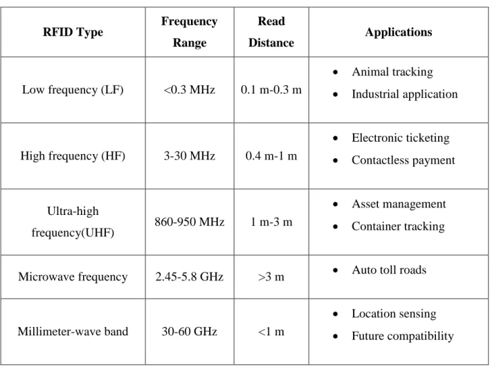
The operating frequency in RFID systems determines the application fields as shown in Table 1-1. Generally, the higher the operating frequency is, the greater the reading range becomes. For low frequency (LF) RFID systems, the 125 kHz or 134 kHz band are assigned in most of the countries. For high frequency (HF) RFID systems, countries have reached the agreement for the use of 13.56 MHz. However, for the ultra-high frequency (UHF) range, different countries have allocated different operating frequency bands. In European Union, the frequency range is from 865 to 868 MHz, in North America it is from 902 MHz to 928 MHz, while in Australia it is from 920 MHz to 926 MHz. China has approved the bandwidth from 840.25 MHz to 844.75 MHz and 920.25 MHz to 924.75 MHz for the RFID technology.
Table I-1 Operating frequency of RFID systems
RFID Type Frequency
Range Read Distance Applications Low frequency (LF) <0.3 MHz 0.1 m-0.3 m Animal tracking Industrial application High frequency (HF) 3-30 MHz 0.4 m-1 m Electronic ticketing Contactless payment Ultra-high frequency(UHF) 860-950 MHz 1 m-3 m Asset management Container tracking
Microwave frequency 2.45-5.8 GHz >3 m Auto toll roads
Millimeter-wave band 30-60 GHz <1 m
Location sensing Future compatibility
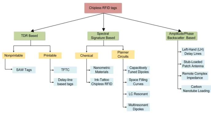
Based on the type of modulation, chipless RFID tags could be categorized into three general types as shown in Figure 1.3[7, 8].
Chipless RFID tag based on time-domain reflectometry (TDR) technique. Chipless RFID tag based on spectral signature.
Chipless RFID tag based on amplitude/phase domain modulation.
For the chipless TDR-based RFID tags, the reader sends the interrogation signal with the time width of ∆T and listens to the echoes from the tag, the tag will generate a train of pulses by adding discontinuities in the transmission line to encode the bits information. The advantages of this kind of tag are low cost, narrow bandwidth, location sensing and greater reading range, etc. The disadvantages of these tags are related to a limited encodable number of bits, and the requirement of high-speed reader RF front-ends to generate the pulse signal.
For the chipless spectral signature-based tag, the reader sends the swept-frequency signal based on the operating frequency of the system and listens to the echo from the tag. The tag generates the encoded data in the spectrum by using resonant structures, the presence of the resonant part means binary code “1”, and the absence of the resonant part means the binary code “0”. The advantages of this kind of tag could be concluded as greater data storage, full printable and low cost, and the disadvantage of this kind of tag is that large bandwidth is required for encoding the information.
For the chipless amplitude/phase-based tag, the tag encodes the data by varying the amplitude and the phase of the backscattered signal. The advantage of this kind of tag is the narrow bandwidth requirement during the operation, and the disadvantage of this kind of tag is the requirement of high resolution of the phase for the reader part to read more bits information.
Millimeter-wave identification (MMID) upgrades the operation frequency to millimeter-wave range. Compared with the conventional RFID system operating at low frequency, the MMID system has the following advantages:
The wavelength of millimeter wave is much shorter, which reduces the size of the integrated antenna. Furthermore, the short wavelength makes it possible to design a small directive antenna array, which can achieve the function of location sensing.
Over the millimeter-wave frequency band, higher data rate (higher than gigabit) communication can be implemented, making it possible for the mass memory transmission over a very short distance.
Applications such as automotive radars have been used over millimeter-wave range, which is possible to be used as MMID readers to detect the MMID tag.
Over the millimeter-wave bands, its effective wavelength is close to the size of a CMOS die, which offers the possibility to integrate the antenna, the MMID tag and the rectifier on the same chip [9].
The MMID concept offers a compatibility with the future applications over millimeter-wave band, such as 5G platform, etc.
A considerable amount of research works on the chipless RFID tag design have been done during the last decade. In [10], transmission delay line was used to build the tag with four bits information at 915 MHz, SAW tag was proposed due to its unique feature of piezoelectric materials which enables much slower surface acoustic waves [11]. In [12], a fully printable planar chipless MMID tag was proposed at 30 GHz, and the tag encodes the data into a spectral signature by using multiresonator. This MMID tag comprises of a multiresonating circuit with 6 spiral resonator and two cross-polarized UWB monopole antennas, but a large bandwidth is occupied during the operation (24 GHz to 36 GHz) and no experimental results were reported in the article. In [13], a 6-bits chipless MMID tag was proposed at 25 GHz, and this MMID tag comprises of 2 orthogonally polarized slot loaded circular patch antennas, which are connected by a right angle transmission line. The resonant frequency is determined by the slot on the patch, hence the number of the identification data bit. In [14], a novel compact chipless MMID tag was presented, and this MMID tag consists of a slot etched on the top of the circular Substrate Integrated Waveguide (SIW) cavity, multi-numbered bits are achieved by adding an array of cavities with frequency and polarization diversity. The challenge is in the reader part, which must be accurate enough to distinguish those very close frequencies and thus the cavities need to achieve a very narrow resonance in order to maximum the encodable number of bits at the fixed bandwidth.
However, previous works on TDR RFID tags were focused on the low-frequency and the works on chipless MMID tags were based on the spectral signature modulation. MMID tags based on TDR technique and phase-domain modulation have not been studied due to the high loss. In this
work, the SIW will be studied to explore the world of MMID, and the thesis is organized in the following way:
In chapter 1, the operating principle of the TDR MMID system is introduced. The theory of lossy transmission line is studied, and the way of encoding bits information in the tag is illustrated. The interval between the bits of information is set considering the distortion issue. A generalized theoretical model is built considering the multireflection issue during the TDR RFID tag design. The link budget is investigated to define the Minimum Detectable Power (MDP) of the system. An equalization method is proposed based on the theoretical modelling as well as the link budget of the system in order to maximize the encodable bits of the tag.
In chapter 2, the studies of the SIW are discussed and reviewed. The interrogation signal distortion caused by the dispersion issue is studied, the meander-line SIW MMID tag is designed and simulated, and the measurement setup is constructed in order to read the proposed tag. HMSIW that can reduce the SIW width by half is investigated. The meander-line HMSIW MMID tag is designed, simulated and measured. Slow-wave substrate integrated waveguide (SW-SIW) is investigated to reduce the group velocity and the slow-wave effect is achieved by the blind vias array which separates the electric field and the magnetic field, and the meander-line SW-SIW MMID tag is designed and simulated. A novel slow-wave half mode substrate integrated waveguide (SW-HMSIW) is proposed to minimize the size of the MMID tag, and the meander-line SW-HMSIW tag is designed and simulated. Finally, the comparison of these four types of tags is conducted to show the difference.
In chapter 3, the operating principle of the MMID system based on the phase modulation is introduced. The SIW phase shifter is proposed by adding the stubs in H-plane which could cover the phase shift range from 0° to 180°. The resolution of 45° is selected to build the tag, two cross-polarized slot antennas are integrated to the two ports of SIW phase shifter in order to avoid the interaction between them. Reader concept based on the VNA together with the two horn antennas is proposed to demonstrate the proposed technique.
The contribution of this work is summarized in the last part. Firstly, the generalized theoretical modelling is adopted for the multireflection issue during the TDR tag design. Secondly, the proposed equalization method is used to maximize the encodable bits of the tag. Thirdly, the MMID tags based on both time domain modulation and phase modulation are studied and measured, showing the feasibility of the MMID system.
CHAPTER 1
EQUALIZATION METHOD FOR CHIPLESS TDR RFID
TAG
1.1 Introduction
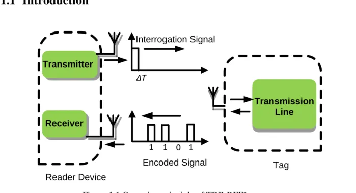
Figure 1.1 shows the operating principle of the chipless RFID system based on time-domain reflectometry (TDR) technique. This system consists of two main components: reader device and transmission line based RFID tag. The transmission line could be microstrip line, coaxial line or other kinds of transmission line. The tag attached on the object can generate a unique ID code. During the operation, the reader sends the interrogation signal (usually a short-pulse signal with fixed time width ∆T), then the signal will be received by the tag antenna. With a calculated transmission length, the received signal will transmit through a fixed delay. By adding discontinuities during the transmission, it will cause the reflected waves at the fixed time position, which are used for coding the unique binary code, then the encoded signal will be transmitted back through the antenna. Finally, the reader will receive the signal back and extract the ID code, which is also called “On-Off keying (OOK) modulation”.
ΔT Receiver Transmitter Reader Device Interrogation Signal Encoded Signal Transmission Line Tag 1 1 0 1
1.2 Transmission line equations
1.2.1 Lossy transmission lines
A uniform lossy transmission line can be represented by a “distributed circuit”, which is divided into an infinite number of cells with infinitesimal length dz. Every infinitesimal cell consists of conductor resistance (R), series inductance (L), leakage capacitance (C) and leakage conductance (G) as shown in Figure 1.2[15].
Parameter L represents the series inductance per cell of the transmission line, R represents the series resistance per cell of the transmission line, C represents the shunt capacitance per cell of the transmission line, and G represents the shunt conductance per cell of the transmission line.
The voltage and the current at z and z+∆z can be expressed as: KVL v(z, t) − R∆zi(z, t) − L∆z∂i(z, t) ∂t = v(z + ∆z, t) (1.1) Load R G R G L C L C dz dz V(z,t) I(z,t) Load
z
dz(a)
(b)
Figure 1.2 (a) A uniform transmission line (b) Distributed circuit representation of transmission lines
KCL
𝑖(𝑧, 𝑡) − 𝐺∆𝑧𝑣(𝑧 + ∆𝑧, 𝑡) − 𝐶∆𝑧 (1.2) Assuming the length ∆z→0, the KVL and KCL equations can be expressed as:
𝜕𝑣(𝑧, 𝑡) 𝜕𝑧 = −𝑅𝑖(𝑧, 𝑡) − 𝐿 𝜕𝑖(𝑧, 𝑡) 𝜕𝑡 (1.3) 𝜕𝑖(𝑧, 𝑡) 𝜕𝑧 = −𝐺𝑖(𝑧, 𝑡) − 𝐶 𝜕𝑣(𝑧, 𝑡) 𝜕𝑡 (1.4) Equations (1.3) and (1.4) are the time-domain transmission line equations, where the voltage and the current on the line are formulated in terms of the position and the time.
For instantaneous voltage and current, it can be expressed as a function of phasor such that: 𝑣(𝑧, 𝑡) = 𝑅𝑒{𝑉(𝑧)𝑒𝑗𝑤𝑡} (1.5)
𝑖(𝑧, 𝑡) = 𝑅𝑒{𝐼(𝑧)𝑒𝑗𝑤𝑡} (1.6)
The derivatives of voltage and the current can be represented in terms of the phasor in equations (1.7) and (1.8), which are also regarded as “frequency-domain transmission line equations”.
𝑑𝑉(𝑧)
𝑑𝑧 = −(𝑅 + 𝑗𝑤𝐿)𝐼(𝑧) (1.7) 𝑑𝐼(𝑧)
𝑑𝑧 = −(𝐺 + 𝑗𝑤𝐶)𝑉(𝑧) (1.8) Taking the derivatives of the above equations with respect to z.
𝑑2𝑉(𝑧) 𝑑𝑧2 = −(𝑅 + 𝑗𝑤𝐿) 𝑑𝐼(𝑧) 𝑑𝑧 (1.9) 𝑑2𝐼(𝑧) 𝑑𝑧2 = −(𝐺 + 𝑗𝑤𝐶) 𝑑𝑉(𝑧) 𝑑𝑧 (1.10) Then combine the equations (1.7), (1.8) with the equations (1.9), (1.10), the following equations can be found as:
d2V(z)
d2I(z)
dz2 = (R + jwL)(G + jwc)I(z) = γ2I(z) (1.12)
where 𝛾 is the complex propagation constant of the transmission given by:
𝛾 = √(𝑅 + 𝑗𝑤𝑙)(𝐺 + 𝑗𝑤𝑐) = 𝛼 + 𝑗𝛽 (1.13) The real part 𝛼 of the propagation constant 𝛾 means the attenuation of the signal in the transmission line with the unit of nepers per meter. The imaginary part 𝛽 means the phase constant of the signal in the transmission line with the unit of radians per meter.
Finally, the general solutions for the voltage and current wave equations could be represented as functions of propagation constant 𝛾 and the position z.
𝑉(𝑧) = 𝑉+𝑒−𝛾𝑧+ 𝑉−𝑒𝛾𝑧 (1.14)
𝐼(𝑧) = 𝐼+𝑒−𝛾𝑧+ 𝐼−𝑒𝛾𝑧 (1.15)
where the 𝑉+𝑒−𝛾𝑧 and 𝐼+𝑒−𝛾𝑧 describe the wave transmitted in +𝑧 direction and the 𝑉−𝑒𝛾𝑧 and
𝐼−𝑒𝛾𝑧 describe the wave transmitted in−𝑧 direction.
The characteristic impedance Z0is given by
𝑍0 =
𝑅 + 𝑗𝑤𝑙
𝛾 = √
𝑅 + 𝑗𝑤𝑙
𝐺 + 𝑗𝑤𝑐 (1.16) The wavelength of the waves during the transmission could be found as:
𝜆 =2𝜋
𝛽 (1.17) A key point of designing a TDR based RFID tag is to calculate the speed of electromagnetic wave. The phase velocity accounts for the speed at which a point of fixed phase propagates. For the waveguide with a chosen medium, the phase velocity could be given by:
𝑉𝑝 =𝑤 𝛽 = 𝑤 √𝑘2− 𝑘 𝑐2 (1.18) where: 𝑘 =𝑤 𝑐 √𝜀𝑟 (1.19)
𝑘𝑐 = √(𝑚𝜋 𝑎 ) 2 − (𝑛𝜋 𝑏 ) 2 (1.20)
Parameters a and b mean the width and the height of the rectangular waveguide, m and n represent modes TEmn that propagate in the waveguide, εr is the relative permittivity of the
waveguide.
The group velocity describes the speed at which the electromagnetic wave travels. For the waveguide with a chosen medium, the group velocity is expressed as:
𝑉𝑔 =
𝑐2
𝜀𝑟𝑉𝑝 =
𝑐2𝛽
𝜀𝑟𝑤 (1.21)
Through equations (1.18) and (1.21), it could be found that phase velocity is faster than the group velocity in the waveguide.
Obviously, for the design of tag, we need to use the delay time along transmission line, which means that the exact travelling time needs to be set and the length of the transmission line needs to be calculated, so the group velocity is adopted.
1.2.2 Transmission line discontinuity
For the incident signal, when it encounters a discontinuity in the transmission line, part of its power will be reflected back and other part of the power will continue to travel along the electrical transmission line as shown in Figure 1.3[16].
Parameter Z01 represents the characteristic impedance of the left transmission line, Z02 represents
the characteristic impedance of the right transmission line, Vi represents the voltage of the incident
signal at the boundary, Vt represents the voltage of the transmitted signal at the boundary and Vr
represents the voltage of the reflected signal at the boundary. The reflection coefficient Γ is given by:
𝛤 =𝑉− 𝑉+ =
𝑍02− 𝑍01
𝑍02+ 𝑍01 (1.22) The voltage and power of the reflected power are expressed as:
𝑉𝑟= 𝛤 × 𝑉𝑖 (1.23)
𝑃𝑟 = 𝑉𝑟2/𝑍01 = 𝛤2𝑃𝑖 (1.24)
The voltage and power of the transmitted power are expressed as:
𝑉𝑡 = (1 − 𝛤)𝑉𝑖 (1.25)
𝑃𝑡 = 1 − 𝑃𝑟 = (1 − 𝛤2)𝑃
𝑖 (1.26)
The method of adding the discontinuity in the transmission line is employed to encode the bits of information in the TDR RFID tag design.
1.2.3 Multireflection issue
For the design of a TDR RFID tag with more than one bit of information, more than one discontinuity should be placed along the transmission line with the same interval for encoding the binary code, which will bring up the multireflection issue. For example, the multireflection issue of tag with four discontinuities is shown in Figure 1.4, Vi represents the amplitude of the incident wave, 𝛤1, 𝛤2, 𝛤3, 𝛤4 represent respectively the reflection coefficients of the first, second, third and fourth discontinuities, 𝑉1, 𝑉2, 𝑉3, 𝑉4 represent respectively the amplitude of the first, second, third
and the fourth reflected waves, R represents the interval between two discontinuities, and Z represents the distance from the excitation to the first discontinuity.
By utilizing the equations (1.14), (1.25) and (1.26), the amplitude of 𝑉1, 𝑉2, 𝑉3, 𝑉4 could be expressed in terms of propagation constant γ, position z, reflection coefficients 𝛤1, 𝛤2, 𝛤3, 𝛤4 and interval between the two discontinuities R as follows:
𝑉1 = 𝛤1𝑒−𝛾𝑧 (1.27) 𝑉2 = (1 − 𝛤12)𝛤 2𝑒−𝛾(𝑧+2𝑅) (1.28) 𝑉3 = (1 − 𝛤12)𝛤22𝛤1𝑒−𝛾(𝑧+4𝑅)+ (1 − 𝛤12)(1 − 𝛤22)𝛤3𝑒−𝛾(𝑧+4𝑅) (1.29) 𝑉4 = (1 − 𝛤12)(𝛤 1𝛤2)2𝛤2𝑒−𝛾(𝑧+6𝑅)+ (1 − 𝛤12)(1 − 𝛤22)𝛤2𝛤32𝑒−𝛾(𝑧+6𝑅)+ (1 − 𝛤12)(1 − 𝛤 22)(1 − 𝛤32)𝛤4𝑒−𝛾(𝑧+6𝑅) (1.30)
1.2.4 Design equations for TDR RFID tag
In the RFID system based on TDR technique, the tag could be regarded as one-port component. The integrated antenna is not only used for receiving the interrogation signal but also for reflecting back the encoded signal. Assuming tt represents the total transmission time from the integrated
antenna to the terminal of the tag, tr represents the transmission time between two discontinuities,
n is the number of the bits of information, ts represents the time width of the interrogation signal,
t0 means the time from the antenna to the first discontinuity, tf means the transmission time in the
free space, ta represents the duration of system operation, the relationship among them should be
arranged as Figure 1.5 shows.
where:
𝑡𝑎 = 2(𝑡𝑓+ 𝑡0+ 3𝑡𝑟) (1.31) 𝐿 = 3𝑅 + 𝑍 = 𝑡𝑡𝑉𝑔 = (3𝑡𝑟+ 𝑡0)𝑉𝑔 (1.32) 2𝑡𝑟 > 𝑡𝑠 (1.33) Equation (1.31) means that because the reader sends the interrogation signal and listens to the echoes from the tag, parameters tf, t0 and tr will be doubled. Equation (1.32) represents the
calculation of total transmission length L of the tag. Equation (1.33) is arranged in order to distinguish the two neighbouring bits of information.
1.2.4.1 Interrogation signal
Generally, the time width of the interrogation signal ts will affect the size of the tag and the
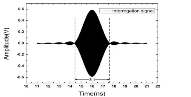
bandwidth of it will determine the bandwidth of the tag antenna. Nowadays, the commercial reader device could generate a 2 ns time width pulse signal, so this pulse signal with the carrier of 35 GHz is considered as the interrogation signal of the system. The waveform and the spectrum of it could be expressed in Figure 1.6 and Figure 1.7.
Figure 1.6 Interrogation signal
1.2.4.2 Interval between two neighbouring discontinuities
In the TDR MMID tag design, the doubled transmission time 2tr should be larger than the time
width of the interrogation signal ts in order to distinguish the two neighbouring “1” information,
and tr should be as small as possible in order to reduce the tag size.
In RFID system, the interrogation signal will encounter some distortion upon received by the tag antenna. Over the millimeter-wave band, it is possible to design the antenna with 1 GHz bandwidth, and after the interrogation signal received by the antenna with 1 GHz bandwidth, assuming the antenna acts as a perfect bandpass filter, the waveform of the signal in frequency domain and in time domain could be evaluated as in Figure 1.8 and Figure 1.9.
Through Figure 1.8, it can be found that after received by the antenna with 1 GHz bandwidth, the high frequency and the low frequency are attenuated, central frequency of 35 GHz with 1 GHz bandwidth remains the same. Through Figure 1.9, the mutation from “0” to “1” of the interrogation signal is disappeared which is replaced by the smooth curve from “0” to “1”, and the time width of the signal is expanded from 2 ns to 3 ns. In order to decode the two neighbouring “1” information,
tr should be at least 0.5 ns to read the binary code “11” as shown in Figure 1.10.
Figure 1.9 Interrogation signal received by tag antenna (time-domain)
1.3 Equalization method
1.3.1 Theoretical modelling
In order to deal with the existing multireflection issue during the TDR MMID tag design, a theoretical modelling is developed by adopting the equations (1.27-1.30). In this modelling, the time width of the interrogation signal ts=2 ns, the transmission time of the interval between two
neighbouring discontinuities tr =0.5 ns and the transmission time from the antenna to the first
discontinuity t0=0.1 ns. For the 4-bits TDR MMID tag design as an example in this work, the
amplitude of the four reflected wave could be expressed as follows: The first reflected wave:
𝑉1 = 𝛤1× 𝑒−(𝛼+𝑗𝛽)×0.1𝑉𝑔×10
−9
(1.34) The second reflected wave:
𝑉2 = (1 − 𝛤12) × 𝛤2× 𝑒−(𝛼+𝑗𝛽)×3.1×𝑉𝑔×10−9 (1.35)
The third reflected wave: 𝑉3 = (1 − 𝛤12)𝛤22𝛤 1𝑒−(𝛼+𝑗𝛽)×6.1×𝑉𝑔∗10 −9 + (1 − 𝛤12)(1 − 𝛤22)𝛤 3𝑒−(𝛼+𝑗𝛽)×6.1×𝑉𝑔×10 −9 (1.36) The fourth reflected wave:
𝑉4 = (1 − 𝛤12)(1 − 𝛤22)(1 − 𝛤32)𝛤4𝑒−(𝛼+𝑗𝛽)×9.1×𝑉𝑔×10 −9 + (1 − 𝛤12)(𝛤 12𝛤22)𝛤2𝑒−(𝛼+𝑗𝛽)×9.1×𝑉𝑔×10−9 + (1 − 𝛤12)(1 − 𝛤 22)𝛤2𝛤32𝑒−(𝛼+𝑗𝛽)×9.1×𝑉𝑔×10 −9 (1.37) where parameters α and β represent the attenuation constant and the phase constant of the transmission line, Vg represents the group velocity and Γ1, Γ2, Γ3, Γ4 represent the reflection
coefficient of the four discontinuities.
In the case of Γ1, Γ2, Γ3, Γ4 equal to 0.25, the amplitude of the interrogation signal equals to 1
and α=1.6 neper/m, β= 1000 rad/m, Vg=1.5×10^8 m/s, the amplitude of the reflected wave can be
Through Figure 1.11, the amplitude of reflected wave will decrease with time, so the information encoded in the subsequent bits will be lost since they are below the minimum detectable power (MDP) of the system. It could be found that the amplitude of the first two bits are higher than MDP, it is possible to transfer part of power from the early bits to the subsequent bits to maximize the encodable bits of the tag.
1.3.2 Lsqcurvefit
Lsqcurvefit is one kind of optimization method in Matlab which is used to solve the nonlinear curve-fitting (data-fitting) problems in a least-squares sense, it could be expressed as [17, 18].
min 𝑥 ‖𝐹(𝑥, 𝑥𝑑𝑎𝑡𝑎) − 𝑦𝑑𝑎𝑡𝑎‖2 2 = min 𝑥 ∑(𝐹(𝑥, 𝑥𝑑𝑎𝑡𝑎𝑖) − 𝑦𝑑𝑎𝑡𝑎𝑖) 2 (1.38) 𝑖
where x is variable that defines the value of 𝐹(𝑥, 𝑥𝑑𝑎𝑡𝑎𝑖), which has the lower and upper bounds
lb and ub, 𝐹(𝑥, 𝑥𝑑𝑎𝑡𝑎𝑖) is regarded as the input of the method, 𝑦𝑑𝑎𝑡𝑎𝑖 is considered as the goal of the optimization. All the parameters can be vectors or the matrices, for 𝐹(𝑥, 𝑥𝑑𝑎𝑡𝑎𝑖) and 𝑦𝑑𝑎𝑡𝑎𝑖, they need to have the same length during the operation.
1.3.3 Equalization method
The equalization method is proposed in this work based on the above-presented theoretical modelling and “lsqcurvefit” in order to maximize the encodable bits of the tag.
In this method, the parameters should be set as follows:
𝑥 = [𝛤1, 𝛤2, 𝛤3, 𝛤4 ] (1.39) 𝑥𝑑𝑎𝑡𝑎 = [𝑉1, 𝑉2, 𝑉3, 𝑉4] (1.40) 𝑙𝑏 = [0,0,0,0] (1.41) 𝑢𝑏 = [1,1,1,1] (1.42) 𝑦𝑑𝑎𝑡𝑎 = [𝐴(0), 𝐴(0), 𝐴(0), 𝐴(0)] (1.43) where x is set as four reflection coefficients of each discontinuity, xdata is set as the amplitudes of the reflected waves, lb and ub are set as the equation (1.41) and equation (1.42) show because the reflection coefficient has the range from 0 to 1, ydata could be set with respect to the binary code that needs to be encoded. For example, for the binary code “1111”, ydata is set to be “[A, A, A, A]” and for the binary code “1101”, ydata is set as “[A, A, 0, A]”, where A represents the amplitude of the reflected wave.
The advantage of this method is that during operation, we can increase the value of A to increase the value of Γ1, Γ2, Γ3, Γ4, the sign of the end of this optimization method is Γ4=1, which reaches
the upper bound and after the optimization, the maximum value of A is found. The physical meaning of it is the last discontinuity is short-circuited and all the power received by the antenna will be used for encoding the bits of information, A represents the maximum amplitude of the reflected wave. Meanwhile, the exact value of each reflection coefficient Γ1, Γ2, Γ3, Γ4 could be
extracted through the matrix x.
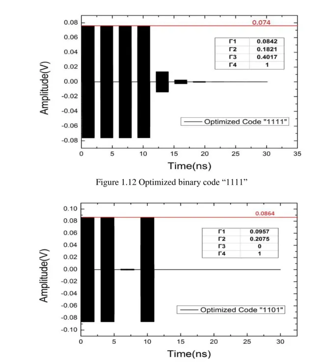
By applying this equalization method to the non-optimized amplitude of the reflected wave in Figure 1.11, the optimized results of the binary code “1111” and the binary code “1101” could be calculated as shown in Figure 1.12 and Figure 1.13.
Through the above figures, we can find that “0.074” is the maximum amplitude for the binary code “1111” and “0.0864” is the maximum amplitude for the binary code “1101”. The reflection coefficient of each discontinuity for generating the results is also tabulated in the figures, and compared with the non-optimized results, two more bits of information could be detected.
Figure 1.13 Optimized binary code “1101” Figure 1.12 Optimized binary code “1111”
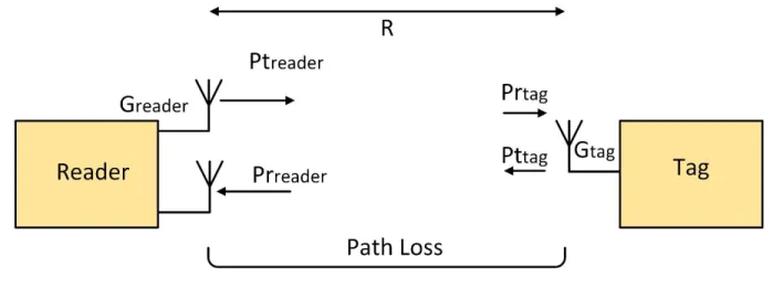
1.4 Link budget of TDR MMID system
The link budget is used for calculating all the gains and the losses from the transmitter to the receiver, it describes the power of the RF signal at any point of the system. The link budget of a passive TDR MMID system is easy to get analyzed because the receiver (tag) has no on-board power supply, it only relies on the power from the reader for encoding the bits of information. The goal of the investigation is to find the power received by the tag and the power finally reflected back to the reader at the particular condition. Furthermore, it will help define MDP of the system [19-23].
Figure 1.14 shows the schematic of the link budget in a TDR MMID system, where 𝑃𝑡𝑟𝑒𝑎𝑑𝑒𝑟
represents the power transmitted from the reader, 𝑃𝑟𝑡𝑎𝑔 represents the power received by the tag, 𝐺𝑟𝑒𝑎𝑑𝑒𝑟 represents the gain of the reader antenna, 𝐺𝑡𝑎𝑔 represents the gain of the tag antenna, 𝑃𝑟𝑟𝑒𝑎𝑑𝑒𝑟 represents the power finally received by the reader, R represents the distance between the
tag and the reader.
Typically, the link budget of the MMID system could be evaluated by the famous Friis equation, which can describe the power transmission between two antennas in ideal case [24].
The power received by the tag can be expressed as follows:
𝑃𝑟𝑡𝑎𝑔 = 𝑃𝑡𝑟𝑒𝑎𝑑𝑒𝑟+ 𝐺𝑟𝑒𝑎𝑑𝑒𝑟+ 𝐺𝑡𝑎𝑔+ 20𝐿𝑜𝑔(𝜆 4𝜋𝑅⁄ ) (1.44)
The power finally received by the receiver can be expressed as follows: Figure 1.14 Link budget of TDR RFID system
𝑃𝑟𝑟𝑒𝑎𝑑𝑒𝑟 = 𝑃𝑡𝑡𝑎𝑔+ 𝐺𝑟𝑒𝑎𝑑𝑒𝑟+ 𝐺𝑡𝑎𝑔+ 20𝐿𝑜𝑔(𝜆 4𝜋𝑅⁄ ) (1.45)
The relationship between 𝑃𝑟𝑡𝑎𝑔 and 𝑃𝑟𝑟𝑒𝑎𝑑𝑒𝑟 can be expressed as follows:
𝑃𝑡𝑡𝑎𝑔 = 𝑃𝑟𝑡𝑎𝑔× 𝑒−𝛼𝑧× 𝛤
𝑖2 𝑖 = 1,2,3,4 (1.46)
where α represents the attenuation constant of the transmission line, 20𝐿𝑜𝑔(𝜆 4𝜋𝑅⁄ ) represents the path loss in the MMID system, and Γi (𝑖 = 1,2,3,4) represents the reflection coefficient of each
discontinuity.
The characteristics of the TDR MMID system is tabulated in Table 1-1, the sensitivity of the reader is set to be -80 dBm, which is available in today’s market, the gain of reader antenna is set to be 20 dBi, which is possible to be realized by the use of a horn antenna, the gain of the tag antenna is set to be 5 dBi, which is also possible to be designed at 35 GHz.
Table 1-1 Characteristics of TDR MMID system
𝑷𝒕𝒓𝒆𝒂𝒅𝒆𝒓 𝑷𝒓𝒓𝒆𝒂𝒅𝒆𝒓 𝑮𝒓𝒆𝒂𝒅𝒆𝒓 𝑮𝒕𝒂𝒈 Frequency
-80 dBm 10 dBm 20 dBi 5 dBi 35 GHz
By applying the equation (1.44), the power received by the tag based on the characteristics in Table 1-1 versus the distance could be calculated in Figure 1.15. As shown here, the power received by the tag will decrease with the distance.
By applying the equation (1.45), the minimum power that needs to be reflected back from the tag to ensure the encoded bits of information detectable versus the distance could be calculated in Figure 1.16, it could be found that the value will increase with the distance.
Figure 1.15 Power received by the tag
With the two values as discussed above, the ratio K between the minimum amplitude of the reflected signal Vttag and the amplitude of the signal received by the antenna Vrtag could be calculated by equation (1.47), and the relationship versus the distance is shown in Figure 1.17.
𝐾 = √10𝑃𝑡𝑡𝑎𝑔⁄10⁄10𝑃𝑟𝑡𝑎𝑔⁄10 (1.47)
The MMID tag could be regarded as a black box as shown in Figure 1.18. In the previous equalization method, the Vrtag is normalized to 1, so the following design rule needs to be satisfied in order to ensure the encoded bits of information detectable.
Design rule:
𝐴 ≥ 𝐾 (1.48) Figure 1.17 Ratio between Vttag and Vrtag
1.5 Maximum encodable bits
Based on the above analysis, a combination of the equalization method and the link budget of the TDR MMID system is proposed to maximize the encodable bits in the tag, which is processed by the following steps.
Build the theoretical modelling of multireflection issue based on the capacity of the tag N. In the equalization method, by adjusting the value of A to make the reflection coefficient of the last discontinuity ΓN = 1, then the maximum amplitude of the reflected signal A is
obtained.
Based on the characteristic of the MMID system, the power received by the tag and the minimum power that needs to be reflected back could be found, and the ratio K between
Vttag and Vrtag versus the distance could be extracted.
Set the condition that 𝐴 = 𝐾, which means the maximum power of the bits of information equals to the Minimum Detectable Power (MDP) of the system. At a fixed distance, the maximum encodable bits could be found which equals to the length of the matrix ydata. In order to verify the proposed method, the characteristic of the MMID system discussed above is considered as an example. Following the above-described execution and design procedure, the
yielded result is shown in Figure 1.19.
As shown in Figure 1.19, the maximum encodable bits versus the distance will decrease with the range of the TDR MMID system, showing the feasibility of this proposed method. For example, at the fixed distance of 1 m, the maximum encodable bits for the tag is “4”, but for the fixed distance of 2 m, the maximum encodable bits is reduced to “3”.
CHAPTER 2
CHIPLESS MMID TAG BASED ON TDR MODULATION
2.1 Full-mode substrate integrated waveguide tag
2.1.1 Introduction
The substrate integrated waveguide (SIW) has received great interest in designing the components over millimeter-wave band in the past few decades [25] [26]. With this technique, passive components and active devices could be integrated in the same printed circuit board (PCB), which leads to the minimization of system size. Moreover, the SIW structure has a similar propagation constant as the classical rectangular waveguide, which offers the benefits of high-Q, high power capability and easy integration etc. Compared with the cost of traditional waveguide, SIW fabrication is cheaper which ensures the possibility of a mass-production of millimeter-wave integrated circuits.
Figure 2.1 shows the geometry of SIW, h represents the height of substrate, w represents the physical width of waveguide, d represents via diameter and s is the spacing between two adjacent vias. It is one kind of rectangular waveguide which is formed by the top metal layer and the bottom metal layer with the substrate sandwiched between them, the two bilateral sides are rows of periodic
metal vias which could be regarded as equivalent electrical walls, and the spacing between the two vias will affect the amount of leakage power during the transmission.
The transverse electric (TE) modes have no electric field in the direction of propagation and the transverse magnetic (TM) modes have no magnetic field in the direction of propagation. Due to the gaps between the metal vias, only TEmn modes are supported in the SIW structures.
According to [27, 28], the effective width of SIW is calculated by the equation (2.1) 𝑤𝑒𝑓𝑓 = 𝑤 − 1.08𝑑2
𝑠 + 0.1 𝑑2
𝑤 (2.1) The cut-off frequency of rectangular waveguide could be calculated by the equation (2.2)
𝑓𝑐 = 𝑐 2𝜋√𝜀𝑟√( 𝑚𝜋 𝑎 ) 2 + (𝑛𝜋 𝑏 ) 2 (2.2)
where 𝜀𝑟 represents the dielectric constant of the substrate, m and n represent the modes transmitted in the structure, a represents the width of the waveguide and b represents the height of the waveguide. In particular, the fundamental mode in SIW structure is the TE10 mode, by combining
the equation (2.1) with equation (2.2), the cut-off frequency of SIW structure could be evaluated in equation (2.3).
𝑓𝑐 = 𝑐
2𝑤𝑒𝑓𝑓√𝜀𝑟 (2.3)
The bandwidth of the fundamental mode in SIW is from 𝑓𝑐 to nearly 2𝑓𝑐. For the MMID tag based on the Rogers 6002 with the dielectric permittivity of 2.94, the minimum effective width is calculated to be 2.88 mm at 35 GHz. In order to avoid the propagation of potential higher modes, the SIW width is considered to be 4.2 mm.
2.1.2 Extraction of propagation constant of SIW
In order to characterize the modes supported in the SIW and to extract its propagation constant, the SIW model is simulated in the Ansoft High Frequency Structure Simulator (HFSS). The dielectric filled in the waveguide is Rogers 6002 with the thickness of 20mil, which has the dielectric permittivity of 2.94. The dimensions of the waveguides are tabulated in Table 2-1.
Table 2-1 Dimensions of SIW
d s h w
0.6 mm 0.9 mm 20 mil 4.2 mm
Figure2.3 S parameters of SIW transmission line
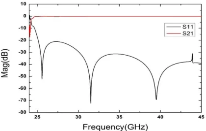
Figure 2.2 shows that the TE10 mode is supported in SIW at 35 GHz and through a full-wave
simulation, forward gain or transmission coefficient S21 and return loss S11 could be calculated in
Figure 2.3, where the cut-off frequency is found to be 25.5 GHz. Figure 2.2 Magnitude of electric field in SIW
2.1.2.1 Attenuation constant αsiw
In [29], the loss in SIW could be concluded as the total contribution of: conductor loss αc,
dielectric loss αd and radiation loss αr. The conductor loss and the dielectric loss are similar to the
traditional rectangular waveguide, but the radiation loss is a unique characteristic of SIW.
2.1.2.1.1 Conductor loss αc
The conductor loss in SIW is caused by the finite conductivity in the top and bottom metal layer as well as the metal vias, by adopting the formula derived for the rectangular waveguide, the conductor loss αc could be calculated with equation (2.4).
𝛼𝑐 = √𝜋𝑓𝜀0𝜀𝑟 ℎ√𝜎𝑐 1 +2(𝑓0⁄ )ℎ𝑓 𝑤𝑒𝑓𝑓 √1 − (𝑓0⁄ )𝑓 2 (2.4)
where 𝜀𝑜 represents the dielectric permittivity of vacuum, 𝜀𝑟 represents the relative dielectric permittivity of substrate, h represents the thickness of SIW, 𝜎𝑐 represents the metal conductivity,
and 𝑤𝑒𝑓𝑓 represents the equivalent width of SIW.
2.1.2.1.2 Dielectric loss αd
The dielectric loss in SIW is caused by the dielectric filled in the rectangular waveguide, same as conductor loss, by adopting the formula derived for the rectangular waveguide, the dielectric loss could be calculated with equation (2.5).
𝛼𝐷 = 𝜋𝑓√𝜀𝑟
𝑐√1 − (𝑓0⁄ )𝑓 2
𝑡𝑎𝑛𝛿 (2.5)
where 𝑡𝑎𝑛𝛿 represents the loss tangent of the dielectric.
2.1.2.1.3 Radiation loss αr
The radiation loss in SIW is caused by the gaps between the metal vias, the distance of the gaps will determine the power loss due to the radiation. For the reason that this is the unique characteristics in SIW structures, the traditional formula derived for the rectangular waveguide is not available for the calculation. The method based on the analytical decomposition of TE10 mode
𝛼𝑅 = 1 𝑤 (𝑤)𝑑 2.84 (𝑑 − 1)𝑠 6.28 4.85√(2𝑤𝜆 )2− 1 (2.6)
The comparison between the simulated results and the calculated results regarding the total loss in SIW has been given in Figure 2.4.
In Figure 2.4, the red curve represents the calculated results through Matlab, the black curve represents the simulated results by HFSS. It could be observed that the simulated results roughly correspond to the calculated results. Finally, the value of the attenuation constant αsiw=1.68 neper/m
at 35 GHz (the operating frequency of the MMID system) is considered for the equalization method proposed in chapter 1.
2.1.2.2 Phase constant βsiw
The analysis of the phase constant βsiw of SIW is the key point for the MMID tag design because
the value of βsiw will not only determine the group velocity of SIW but also arouse the dispersion
issue.
The phase constant βsiw versus frequency is calculated in Figure 2.5. For the SIW tag design, the
value of the phase constant βsiw=1008 rad/m at 35 GHz is considered for the equalization method
proposed in chapter 1.
2.1.3 Distortion
2.1.3.1 Group velocity of SIW Vgsiw
When the interrogation signal transmits along the SIW, the distortion of the interrogation signal could be divided into two parts: dispersion and attenuation. The group delay 𝜏𝑔𝑠𝑖𝑤 represents the time delay of amplitude envelopes versus frequency in SIW, which could be used to describe the dispersion issue as expressed in equation (2.7).
𝜏𝑔 = −
𝑑(∅(𝑒−(𝛼+𝑗𝛽)𝐿))
𝑑𝜔 (2.7) where ∅(𝑒−(𝛼+𝑗𝛽)𝐿) represents the total transmission radian of the interrogation signal and ω represents the angular velocity.
In order to characterize the distortion issue in SIW, the value of αsiw and βsiw over the frequency
range from 34.5 GHz to 35.5 GHz is extracted through (2.7), we can adjust the value of the Figure 2.5 Phase constant of SIW
transmission length L to make 𝜏𝑔𝑠𝑖𝑤= 3 ns at the centre frequency of 35 GHz, which meets the criteria set in chapter 1.
As Figure 2.6 shows, the red curve represents the attenuation of the signal, which increases with frequency. The black curve represents the group delay of signal, which decreases with frequency. With the optimized L=42.3 cm, the group delay of 3 ns at 35 GHz is generated and it could be observed that the interrogation signal is expanded from 3 ns to 3.08 ns. This level of distortion is acceptable for the interval of 1 ns between two neighbouring pulses.
Then the group velocity of the signal in SIW 𝑉𝑔𝑠𝑖𝑤 can be calculated by the equation (2.8).
𝑉𝑔𝑠𝑖𝑤 =
𝐿
𝜏𝑔 = 1.41 ∗ 10
8 𝑚/𝑠 (2.8)
2.1.3.2 Interrogation signal distortion
The spectrum of the interrogation signal after the transmission length of 42.3 cm could be calculated by (2.9), which is shown in Figure 2.7.
𝑓𝑜 = 𝑓𝑠 ∗ 𝑒−(𝛼+𝑗𝛽)𝐿 (2.9)
Inverse Fourier transform is performed based on the spectrum of the output signal in order to find the output signal in time domain.
Through Figure 2.8, it could be observed that the time delay of the amplitude envelope of 3 ns is achieved with the transmission length of 42.3 cm and the interrogation signal is expanded from 3 ns to 3.08 ns.
Figure 2.7 Spectrum of output signal (SIW)
2.1.4 Meander-line based SIW tag
2.1.4.1 DiscontinuitiesWith the extracted αsiw=1.68 neper/m, βsiw=1008 rad/m and Vgsiw=1.41*108 m/s, by applying the
equalization method proposed in chapter 1, the reflection coefficient of every discontinuity could be calculated and given in Figure 2.9.
There are three methods to create discontinuity through the transmission in SIW such as adding stubs, metal vias or symmetrical iris in H-plane as shown in Figure 2.10.
Figure 2.9 Reflected wave in SIW (Matlab)
For the SIW tag design, the iris in H-plane is considered for encoding the bits of information. The equivalent circuit of this kind of discontinuity is shown in Figure 2.11 [30], its reflection coefficient can cover the range from 0 to 1 by adjusting width w as shown in Figure 2.12.
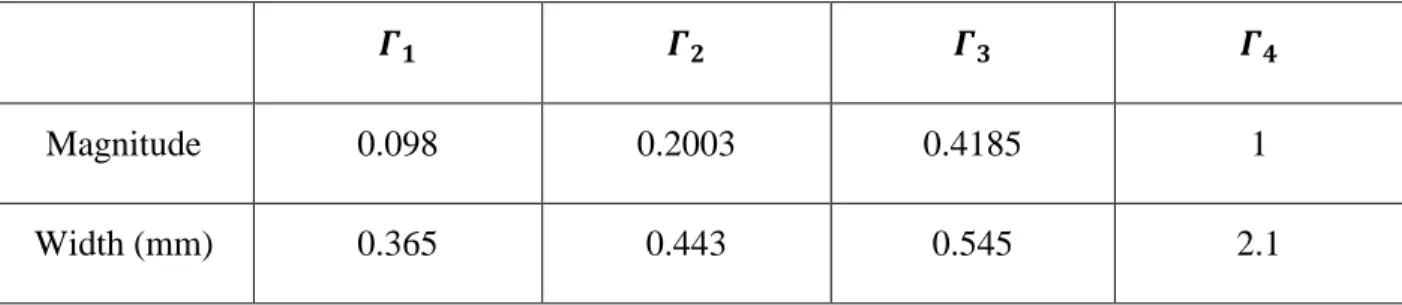
With the value of four calculated 𝛤𝑖 as depicted in Figure 2.9, the dimensions of each iris can be extracted based on the curve in Figure 2.12, which are tabulated in Table 2-2.
Figure 2.11 3 Discontinuity in SIW
Table 2-2 Dimensions of discontinuities (SIW)
𝜞𝟏 𝜞𝟐 𝜞𝟑 𝜞𝟒
Magnitude 0.098 0.2003 0.4185 1
Width (mm) 0.365 0.443 0.545 2.1
2.1.4.2 Antenna of SIW tag
For the SIW tag design, the slot antenna is considered for its integration with the MMID tag. Generally, slots on the waveguide are assumed to have a narrow width (less than 0.1 of wavelength in the substrate) and the length of the slot is 0.5 of wavelength in the substrate [31-33].
Table 2-3 Dimensions of SIW slot antenna
Thickness X_slot Y_slot P_slot
Magnitude 20 mil 0.35 mm 2.1 mm 2.1 mm
Figure 2.13 shows the topology of an SIW slot antenna with the dimensions tabulated in Table 2-3, the model is simulated in HFSS with Rogers 6002 and the substrate thickness is 0.508 mm.
The antenna is proposed to operate at the center frequency of 35 GHz with the bandwidth of 1 GHz as discussed in chapter 1.
Figure 2.14 shows the return loss of the SIW slot antenna, the antenna is operating at the centre frequency of 35 GHz, and the bandwidth is 1 GHz, which meets specification as mentioned above in chapter 1. Figure 2.15 shows the radiation pattern of this antenna with the gain of 6.52 dBi.
Figure 2.14 Return loss of SIW slot antenna