Sensing Applications: Fabrication using
State-of-the-art Laser Micromachining
By
Vinayak Pachkawade
Faculty of Applied Science
Department of Electrical Engineering and Computer Science
University of Liege
This dissertation is submitted for the degree of Doctor of Philosophy
Declaration
I, Vinayak Pachkawade, declare that except where specific reference is made to the work of others, the contents of this dissertation are original and have not been submitted in whole or in part for consideration for any other degree or qualification in this, or any other University. This dissertation contains less than 45,000 words including appendices, bibliography, footnotes, tables and equations and has less than 100 figures.
I further state that
This work was done wholly or mainly while in candidature for a research degree at the University of Liege.
A work in this thesis has attempted to the large extent to comply with the PhD research project that was drafted.
A research presented in this thesis is the result of accumulative work that I have carried out on my own.
A work done in this thesis complies the state-of-the-art in the field. All main resources and supports have been acknowledged.
Parts of this work have been published in: 1) https://doi.org/10.1007/s00542-019-04549-2, and 2) [1].
Vinayak Pachkawade October 2019
Acknowledgements
First, I expressed my sincere and deepest gratitude to the University of Liege for giving me an opportunity to do doctorate. It has been rewarding experience for me to do a PhD amidst thoughtful scientific community in the campus. This research was supported by University of Liege.
I thank my PhD advisor Prof. Dr. Michael Kraft. I learned from him not only about research but also many other things. As I move forward in my life, I adopt positives from him. I also would like to thank members of my thesis committee, Prof. Philippe Vanderbemden, Prof. Tristan Gilet, and Prof. Benoît Vanderheyden for their time, support and being my thesis committee members. Particularly, I thank Prof. Benoît Vanderheyden for his composed, reasonable perspective and support.
I also thank Prof. Guy Leduc, department chair, for his principle based approach and giving me an opportunity to continue my work at the University of Liege.
I extend my thanks to Dr. Serguei Stoukatch, for allowing me access to the Microsys clean room where, I could operate facilities such as optical microscope, wire bonding, etc. I also thanks other members of Microsys group, namely François Dupont, in supporting to arrange lab resources, Samuel Dricot for working with me in fabrication of prototype samples. My thanks goes to one of the skilled technician of Montefiore institute, Mr. Thierry Legros, for continually helping me in circuit board assembly, support in arrangement of lab components at the earliest. I thank Pascal Harmeling for sharing his knowledge on board level electronics. I acknowledge contribution from Delphine Cerica, then my lab mate and now a researcher in the department, with whom I used to discuss the research ideas. I also thank other lab mates for their cooperation during my work.
I show appreciation to many other people who directly/indirectly contributed in my work that I could reach to a stage of writing this dissertation.
I thank my family members, my wife for contributing in my well being, taking good care of my little daughter, Grace while I am at the office, working late hours often, and sometimes even during the weekends.
I thank my mother back in India who lent me her ears in difficult times, whenever I called her. She offered me an incredible sense and support.
Finally, I thank my graceful child Grace, whose delightful presence and charm contributed in supplying me energy and inspiration, to endure and accomplish my goal.
Abstract
This thesis documents a first time demonstration of electromechanical transducer and/or sensor fabricated using Direct Laser Writing (DLW). A low-cost prototype has been fabricated via a rapid and high-tech laser micro-milling technique to achieve a parallel kerf-width (capacitive gaps) of about 60 micrometers (µm) into a piece of aluminum and a stainless steel each of 1 and 2 millimeters (mm) thickness respectively, thus leading to a high-aspect ratio (> 33) structure. A device is demonstrated to facilitate actuation via electrostatic means and sense a capacitive change across its electrode. Experiments have been performed with a structure made of aluminum. Emphasis is on the fabrication and associated issues. A strategic fabrication and measurement of an average kerf-width of about 60 micrometres is reported, which is advantageous to develop our application. A detailed study of width variation using laser cut is also given. Based on the in-depth literature survey, it is postulated that achieving simultaneously a kerf-width as small as 60 µm with metal parts up to 2 mm thickness is unprecedented (either in the industry or in academia). This important aspect is one of the highlights of this research. Results comprising analytical modeling, fabrication, and electrical characterization are presented. An applicability of a device as a 2 degree-of-freedom (DoF) resonating mode-localization sensor that employs a weak electrostatic coupling is demonstrated to offer vibration amplitude based sensitivity to a relative change in the stiffness. This sensor is able to resolve a minimum stiffness perturbation (normalized), kmin
eff k K
of the order of 7.98×10⁻⁴. This magnitude is of the same order to that achievable in MEMS based
coupled resonators. Based on our opening results, it is postulated that this navigating research opens up new possibilities to fabricate new devices and/or sensor based on alternative fabrication platform such as laser micromachining as reported here.
In parallel, a work in this thesis closely observes the state-of-the art for coupled resonators and thereby proposes realistic system level models in the context of our architecture fabricated using high-tech laser machining. Based on the representative system-level models developed in this thesis, theory estimate of maximum sensitivity to stiffness perturbation is found to be comparable to that achievable in MEMS for two degree of freedom (DoF) coupled resonating sensor. Developed models represents findings in open/closed loop implementation. A work on the most fundamental and crucial aspects such as sensitivity, resolution and noise floor of coupled resonators is reported.
Contents
Contents ... ix
List of Figures ... xiii
List of Tables ... xix
1 Introduction ... 22
1.1 Motivation of research ... 22
1.1.1 Principle of electromechanical transduction in micromachined resonators ... 23
1.1.2 Resonator in sensing applications ... 24
1.1.3 A new transduction principle: paradigm shift in resonant sensing applications 25 1.1.4 Potential applications for mode-localized sensors ... 26
1.1.5 Fabrication using the state-of-the-art laser micromachining ... 28
1.2 Thesis organization ... 28
2 Literature Review ... 30
2.1 Electrostatic actuation and capacitive sensing ... 30
2.2 Motional current ... 32
2.3 A mass-spring-damper system... 32
2.4 Transfer function for one DoF system ... 33
2.5 Coupled resonators... 36
2.6 Coupled resonators in sensing applications... 36
3 Theory and Design ... 51
3.1 Device geometry and design parameters ... 51
3.1.1 A MEMS electromechanical transducer design ... 53
3.1.2 A motional resistance estimation in our design ... 56
3.1.3 Choice of material from a design perspective ... 58
3.2 A coupled resonator design (scaled-up architecture) ... 58
3.2.1 Design of a perturbation electrode ... 62
3.3 Theoretical transfer function of our design ... 63
3.3.1 A two DoF coupled mass-spring-damper system ... 63
3.3.2 A three DoF coupled mass-spring-damper system ... 65
3.4 COMSOL design (A finite element model) ... 67
3.5 Performance parameters ... 67
3.6 Dynamic response of our design ... 74
4 System level models and simulation ... 77
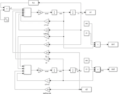
4.1 A Simulink model ... 77
4.2 Operating conditions in our design ... 79
4.2.1 Case I ... 80
4.2.2 Case II ... 84
4.3 Frequency response of our design ... 91
4.4 Impact of Q, Kc and δk in our design ... 92
4.5 Noise analysis in our design ... 95
4.5.1 Noise in a mechanical sensing system ... 95
4.5.2 Noise floor in a mode-localized sensor ... 95
4.5.3 Thermo-mechanical noise in our design ... 95
4.6 Modelling the impact of electronic noise in our design ... 99
4.6.1 Noise analysis in SPICE ... 102
4.6.2 Resolving the lowest possible shifts (i.e. resolution) in our design... 105
4.7 Influence of coupling strength on the effective noise floor ... 106
4.8 Equivalent circuit Models in SPICE ... 107
4.9 Amplitude stability of output signals ... 111
4.9.1 Spectral analysis ... 114
4.10 Closed-loop arrangement ... 117
4.10.1 Design of a PLL ... 118
5 Fabrication ... 121
5.1 Overview of fabrication techniques ... 121
5.1.1 Wire-electro-discharge machining (EDM) ... 121
5.1.2 Additive manufacturing (3D printing) ... 121
5.1.3 Laser micromachining ... 122
5.2 Fabrication at the University of Liege ... 123
5.3 Fabrication with the outside company ... 127
5.3.1 3D AutoCAD file ... 127
5.4 A PCB design for a developed prototype ... 129
5.5 Auxiliary laser cutting for a developed prototype ... 129
5.6 Assembly plan ... 131
5.7 Finalized part ... 132
6 Electrical test and characterization ... 139
6.1 A description of the experimental methodology ... 139
6.2 Device measurements ... 143
6.2.1 Operating point ... 145
7 Discussion, conclusion and future direction ... 148
Appendix A... 153
Appendix B ... 158
Figure 1.1 Electrical equivalent model for a MEMS resonator ... 23 Figure 1.2 (a) A schematic representation of two identical mass-spring-damper system coupled by spring to illustrate transduction principle, (b) graphic showing key performance parameters pertaining to new class of resonant sensor based on mode-localization. ... 26 Figure 1.3 A graphic showing potential sensing applications that can be developed using coupled resonators... 27 Figure 2.1 Electrostatic actuation and capacitive sensing in parallel plate actuator ... 30 Figure 2.2 A mass-spring-damper system. ... 33 Figure 2.3 Magnitude-frequency response of a single DoF mass spring damper system [44] 35 Figure 2.4 Ultrasensitive mass sensor using a mode localization in coupled microcantilevers [16] ... 37 Figure 2.5 A microbeam sensors utilizing mode-localization to detect and identify the analyte [52] ... 38 Figure 2.6 Electrically coupled weakly coupled resonators with enhanced sensitivity (a) A fabricated double-ended tuning fork and (b) two free-free beam resonators and (c) a
representative two DoF coupled resonator model [17] ... 39 Figure 2.7 A coupled resonator sensor employing an array of three resonators [18] ... 40 Figure 2.8 A mode-localized MEMS electrometer based on two mechanically coupled resonators [54] ... 41 Figure 2.9 A mass sensor using two DoF coupled resonators [25] ... 42 Figure 2.10 A cantilever based mass sensor (a) simulated frequency response and (b)
fabricated prototype [60] ... 42 Figure 2.11 In search of optimal mode localization in a mechanically coupled resonators (a) graph showing coupling spring optimization and (b) implemented prototype in a mechanical workshop [62] ... 43 Figure 2.12 An accelerometer based on mode-localization (a) a prototype image and (b) output of an sensor as a function of acceleration [24] ... 44 Figure 2.13 (a) A circuit network of two RLC components, representing two series resonant tanks. A capacitor Cc is the coupling capacitor, coefficient of coupling is set by the ratio
C/Cc. (b) frequency response of the system for three values of perturbation [67,68] ... 45
Figure 2.14 The simulated (a) and measured (b) amplitude difference (AD) amplitude ratio (AR) of the 2nd mode under the Out-Driven scheme [71] ... 46
prototype (b) measurement setup in open loop and (c) measured response [72] ... 47 Figure 2.16 Simulated spectrum of amplitude ratio fluctuations when the system is subject to independent white noise perturbations. Simulation parameters are F=1, ω=1, Q=1000, ε=0 [84,85] ... 48 Figure 2.17 (a) Oscillator schematics including the optical micro-graph of the prototype mode-localized resonant sensor and (b) amplitude ratios variations for varying the normalized stiffness perturbations [88] ... 49 Figure 3.1 (a) A perspective view schematic of a two DoF weakly coupled resonators
highlighting the entire necessary feature. Red dotted lines indicate parallel kerf-widths to be machined through entire device thickness for capacitive transduction. The shaded area in dark blue indicates material to be ablated during machining. As shown, the DC voltages V+ and V− to be applied not only to polarize the individual micro-machined gap capacitors but also couple them through this electric potential difference. (b) 3D view of the design... 52 Figure 3.2 resonant frequency variation as a function of ratio, r. ... 55 Figure 3.3 A variation in a resonator motional resistance for a) a varying beam width, Wb and
b) a varying DC voltage, Vdc. ... 57
Figure 3.4 Variation of coupling spring constant, Kc as a function of thin plate length that is
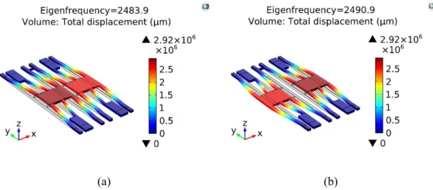
attached to either side of each of the proof mass in a coupled resonating sensor. With higher device thickness, h, it is beneficial to create a larger electrostatic force between the gap coupling two proof masses. ... 60 Figure 3.5 Resonant mode frequencies of a device as a function of a) a varying DC voltage used in the system and b) a normalized coupling factor. Out-of-phase mode frequency always precedes in-phase mode frequency due to negative effective value of a coupling stiffness between the two proof masses. As seen, a specific value of coupling factor helps attain a adequate mode-frequency difference. ... 61 Figure 3.6 Mode-frequency difference as a function of coupling factor in weakly coupled resonators. ... 62 Figure 3.7 A lumped parameter model for a three DoF coupled resonators ... 66 Figure 3.8 A COMSOL mode shape simulation for a structure, (a) mode 1 (in-phase mode) and (b) mode 2 (out-of-phase mode). These two distinct modes are separated by a distance of approximately 7 Hz. An individual resonating element is coupled to its neighbour by a mechanical beam thus emulating an electrical coupling spring in the actual fabricated
prototype ... 67 Figure 3.9 Eigenvalue loci veering ... 70 Figure 3.10 (a) frequency variations as a function of stiffness perturbations. (b) Mode-frequency difference as a function of stiffness perturbations ... 71 Figure 3.11 Variation in the amplitude ratio output as a function of stiffness perturbations .. 71 Figure 3.12 Comparative output performance as a function of stiffness perturbations (a) absolute values (b) in percentage. A comparative performance for all the outputs for damping coefficient (in Ns/m) c0(Q ); k 0 ... 72
conditions with (a) damping coefficient, c set to 0.0016 Ns/m (Q ≈ 5000) and (b) for damping coefficient, c set to 0.0031 Ns/m (Q ≈ 2547). M1 and M2 denote proof mass 1 and 2
respectively, while δk is applied stiffness perturbations (normalized) ... 73
Figure 3.14 Theory model for our two DoF weakly coupled resonating sensor illustrating an impact of a damping for (a) resonator 1 and (b) resonator 2. With higher damping (lower quality factor), two distinct modes overlap. ... 74 Figure 4.1 A system level model (using SIMULINK) for a two coupled resonators to evaluate its performance as a sensor ... 77 Figure 4.2 Simulated power spectrum of our design across the frequency range of interest. Two resonant peaks are seen to be separated by about 7 Hz. Operating conditions are c = 0 Ns/m, (Q→∞), ∆k = 0, κ = -0.0032, unit force, F=1 N exerted on proof mass M1 ... 80
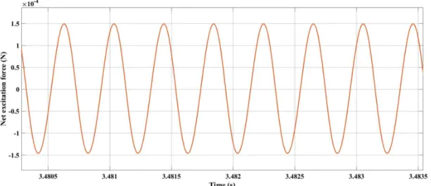
Figure 4.3 Steady-state time-response for a net applied electrostatic force at the out-of-phase excitation frequency, ωop, 2474 Hz. A maximum value of this force is simulated to be ≈ 149
µN. (peak-to-peak is 295 µN) ... 80 Figure 4.4 Steady-state time-response for displacement x1 and x2 from mass M1 and M2
respectively, (a) at the out-of-phase excitation frequency, ωop, 2474 Hz. (b) at the in-phase
excitation frequency, ωip, 2482 Hz. ... 81
Figure 4.5 Steady-state time-response for motional current im1 and im2 from mass M1 and M2 respectively, (a) at the out-of-phase excitation frequency, ωop, 2474 Hz (b) at the in-phase
excitation frequency, ωop, 2482 Hz. ... 82
Figure 4.6 A mode-localization effect in our macro-scale coupled resonators (a) out-of-phase and (b) in-phase mode. x1 and x2 are amplitude of displacement for resonator 1 and 2
respectively. ... 83 Figure 4.7 (a) Output metric for our design of two DoF coupled resonators for the following operating condition: damping coefficient, c = 0 Ns/m; A proof mass M1 is driven at
out-of-phase frequency, ωop which is a function of ∆k, (b) representative equivalent model ... 84
Figure 4.8 Steady-state time-response (a) and (b) at the out-of-phase excitation frequency, ωop, 2474 Hz, (c) and (d) at the in-phase excitation frequency, ωip, 2482 Hz. x1 and x2 are
displacements, im1 and im2 are motional current from mass M1 and M2 respectively. ... 86
Figure 4.9 Simulated power spectrum of our design across the frequency range of interest for finite value of a quality factor. Two resonant peaks are seen to be separated by about 7 Hz. 87 Figure 4.10 A mode-localization effect in coupled resonators (a) and (b) out-of-phase and (c) and (d) in-phase mode. x1 , x2 are amplitudes of displacement and im1, im2 are motional
currents for resonator 1 and 2 respectively, c = 0.0031 Ns/m, (Q ≈ 2547), κ = -0.0032 ... 89 Figure 4.11 A comparative performance for all the outputs for c = 0.0031 Ns/m (Q ≈ 2547); ∆k ≠ 0, κ = -0.0032. A representation for a frequency shift output is shown 10× times scaled up to illustrate a comparison among other outputs. A reasonable match was observed between the simulation and theory. Magnitude of δk used in theory and/or simulations are same as used
during the experiments. A proof mass M1 is driven at out-of-phase frequency, ωop which is a
function of ∆k ... 90 Figure 4.12 A comparative performance for the amplitude ratio based output metric, for c = 0.0031 Ns/m (Q ≈ 2547); ∆k ≠ 0, κ = -0.0032. A representation for a frequency shift output is
is driven at out-of-phase frequency, ωop first and then at the in-phase mode frequency, ωip
(mode frequenies being a function of ∆k) ... 91 Figure 4.13 A simulated frequency response of our design ... 92 Figure 4.14 Simulated output response showing impact of structural damping (a) resonator 1 and (b) resonator 2, operating conditions are F= 1N, Q varying from infinity to about 8, Kc =
-393.51 N/m, δk = 0, Y-axis is log scale ... 92
Figure 4.15 Simulated output response showing impact of structural damping (a) resonator 1 and (b) resonator 2, operating conditions are F= 1N, Q varying from infinity to about 8, Kc =
-100 N/m, δk = 0, Y-axis is log scale ... 93
Figure 4.16 Simulated output response (a) resonator 1 and (b) resonator 2, operating
conditions are F= 1N, Q is about 2547, varying Kc, δk = 0, Y-axis is log scale. ... 93
Figure 4.17 Operating conditions are F= 1N, Q is about 2547, Kc = -393.51 N/m, δk ≠ 0,
Y-axis is log scale ... 95 Figure 4.18 Simulated power spectrum density (PSD) of an displacement noise of resonator 1 and 2 subject to mechanical-thermal noise forcing term on resonator 1. (a) Kc = -393.5 N/m
and (b) Kc = -1000 N/m. Simulation conditions are those reported in section 4.2.2, case 2. .. 97
Figure 4.19 Simulated power spectrum density (PSD) of an displacement amplitude noise in resonator 1 and 2 for varying coupling strength, Kc. ... 98
Figure 4.20 (a) OPA 381 interface with our sensor design (b) equivalent noise circuit to evaluate circuit dominant noise. ... 100 Figure 4.21 (a) OPA 381 interface with our sensor design (b) equivalent input noise current for varying feedback gain, (c) output noise voltage for varying feedback gain, (d) total integrated output noise in rms for varying feedback gain, and (e) output noise density for varying Rx and fixed Rf of 1Meg. ... 104
Figure 4.22 Simulated power spectrum density (PSD) of the motional current output signal in a two weakly macro-scale coupled resonator for the following operating condition, Q = 2547, κ = -0032, δk = 0, F =1 N ... 106
Figure 4.23 Simulated power spectrum density (PSD) of the motional current output signal for varying coupling strength, Kc. electrostatic drive forcing term set to unity ... 107
Figure 4.24 A SPICE analysis: (a) Equaivalent circuit model for our design, (b) Simulated graph of the motional current output signal for fixed coupling strength, Kc, left side of the
graph is magnitude and right side of the graph is phase, (c) frequency response as a function of varying (negatively increasing) coupling strength, Kc varying from -393.51 N/m to -1000
N/m. ... 108 Figure 4.25 An effect of applied perturbations into the coupled resonator model for c = 0.0031 Ns/m, (Q ≈ 2547), ∆k ≠ 0, κ = -0.0032. Applied negative stiffness perturbations vary from -98.37 N/m to -238.37 N/m. ... 109 Figure 4.26 An effect of varying structural damping showing eventually modes being
merged. Effective quality factor varies from 2600 to 10. ... 110 Figure 4.27 Simulated output response of the resonators for varying perturbations.
model is about 410. ... 110 Figure 4.28 A model for the noise analysis in a coupled resonators ... 111 Figure 4.29 Simulated effective noise floor in either of the output channel. A simulated value of effective noise current is ≈ 0.7 × 10⁻¹³ Arms (equivalent to -263 dB for reference load of 1
Ω) ... 112 Figure 4.30 Simulated time-plots of a motional currents im1 and im2 at (a) in-phase mode
frequency, (b) out-of-phase mode frequency. Operating conditions are δk = 0 and (Q =2547).
Added noise level is ≈ 100 pArms ... 113
Figure 4.31 Mode-localization at the in-phase mode frequency, in the presence of a noise into the system. δk= -0.0019 (normalized) Q=2547 approximately. In-phase mode chosen because
it showed better amplitude stability as compared to its out-of-phase mode counterpart ... 114 Figure 4.32 Simulated power spectrum of our design across the frequency range of interest. (a) and (b) with less noise current, (c) and (d) with increased noise current, operating
conditions is given in case II in section 4.2.2. ... 115 Figure 4.33 Simulated power spectrum of our design across the frequency range of interest. (a) and (b) with less noise current, (c) and (d) with increased noise current, operating
conditions is given in case II in section 4.2.2. Y-axis is log-scale. ... 116 Figure 4.34 Simulated PSD and power spectrum plot: For an effective output referred noise (left y-axis) and signal power output (right y-axis) for (a) mode 1 and (b) mode 2 in our two scaled-up weakly coupled 2 DoF architecture ... 116 Figure 4.35 Amplitude noise PSD in our design ... 117 Figure 4.36 Simulink model for a closed loop arrangement ... 118 Figure 4.37 A comparative performance of our design in closed-loop and open loop circuit arrangement. Graphs obtained from the simulation of a model of our macro-scale coupled resonators. ... 120 Figure 5.1 Sample prototype preparation at the University of Liege through laser ablation method. (a) top view , (b) bottom view, and (c) side view ... 123 Figure 5.2 Optical images of a fabricated prototype at the university campus highlighting various device features. (a) metal ablated area, (b) proof masses with beam suspension, (c) electrode to apply electrostatic drive force to proof mass 1, (d) electrode to apply perturbation and (e) kerfs (also called capacitive gaps) ... 125 Figure 5.3 Measurement of a laser cuts (capacitive gaps) in a fabricated prototype ... 126 Figure 5.4 A picture of a finished prototype (a) front view and (b) back view ... 127 Figure 5.5 An AutoCAD diagram (created using Freecad software [139]) showing all the dimensions for the device features. All dimensions are in mm ... 128 Figure 5.6 A device prototype pattern drawn using Freecad software [139], (a) A pattern showing the micro-size capacitive gaps to be fabricated, (b) a 3D representation. ... 128 Figure 5.7 A printed circuit board plan for the developed prototype. (a) drawing pattern and (b) 3D view ... 129 Figure 5.8 A pattern developed using AutoCAD software to perform a supplementary laser milling at the indicated locations on the finished part ... 130
manufacturer, (b) PCB arrangement to support the part as a base, (c) part glued on top of the PCB, and (d) finished part with supplementary laser cutting to electrically isolate sub-parts of a device. ... 132 Figure 5.10 Photograph of a prototype fabricated out of aluminum with thickness, h =1 mm). Ablation zone is an area from where metal has been removed. (a) front view: suspension beams are attached to proof masses at one end and other ends of the beams are fixed on to the base laminate. An electrical connection between device and copper tracks is done through aluminum wedge bonding technique. Copper tracks are subsequently connected to the header connector pins through a wire soldering. (b) back view: a device is fixed onto epoxy laminate (which has a central cut as shown) to allow displacement with the established mechanical boundary conditions. Dashed rectangle shapes indicates the high velocity locations where gap measurements was done. ... 133 Figure 5.11 photographs of a fabricated prototype (a) side view, (b) top view and (c) bottom view. ... 134 Figure 5.12 Images of the prototype (aluminum with 1 mm thickness) acquired through Leica microscope. (a) The top portion, showing electrodes reserved to apply external stimulus to alter the stiffness of the beams of the proof masses. (b) Middle portion showing proof masses separated by a micro-size kerf-width. (c) A close-up view of a clean sharp laser-cut thus forming parallel kerf. (d) Close-up view of one of the measured kerf-width. (One between the two proof masses) ... 135 Figure 5.13 Microscopic images to present quality of laser cut and width variation ... 137 Figure 6.1 (a) A schematic representation of an experimental set-up, (b) illustrates the schematic representation of our design also highlighting possible feedthrough paths in the circuit, and (c) an equivalent circuit model representing the experimental condition for signal measurement. ... 141 Figure 6.2 A set of DC voltages were applied as illustrated. As shown in the inset, DC to high voltage DC converter was used between a power supply and prototype. An AC drive signal was applied (through the internal reference oscillator of lock-in amplifier) to electrode 1 as shown. A frequency sweep around estimated mode-frequencies was performed and output signal (amplitude-frequency response) was recorded through a lock-in amplifier. In our case, a signal form the body of resonating proof mass, M2 was recorded ... 143 Figure 6.3 (a) With AC = 5V, (b) with AC = 2V. A DC voltages, +200V and -200V were applied to proof mass 1 and 2 respectively. Stiffness perturbation was applied to the resonator 2 and an output was recorded from the resonating proof mass 2. Variations in the vibration amplitudes were prominently observed, and (c) SPICE simulated frequency response from the practical circuit model. ... 144 Figure 6.4 Measured vibrational amplitude variations into the output signal of a resonating proof mass 2 for two operational cases, (a) and (c) - when an AC drive signal is set to 2V and, (b) and (d) - when an AC drive signal is set to 5V ... 145 Figure 6.5 Sensitivity to amplitude [0.547% max. shifts in amplitude] was observed to be one order of magnitude higher as compared to sensitivity to frequency [0.038% max. shifts in frequency] (subject to measurement errors) ... 146
Table 1.1 Analogy between mechnical and electrical domains [6]. ... 23
Table 3.1:Design parameters for a developed prototype ... 52
Table 3.2: Detailed calculation for the device. (h represents device thickness) ... 57
Table 3.3 Calculations for performance parameters (h represents device thickness) ... 68
Table 4.1 A system-level model parameters ... 78
Table 4.2 Noise calculations ... 100
Table 4.3 Comparative noise analysis of our design ... 105
Table 4.4 Calculation for applied stiffness perturbations ... 110
Table 4.5: Noise estimation in macro-scale coupled resonator design ... 111
Table 4.6 A frequency tracking table for the comparative purpose. ... 118
Nomenclature
F electrostatic forcing term
Fnoise_rms Noise forcing term (rms)
Fnoise_density spectral density of a noise forcing term
Fnoise_avg mean square amplitude
xji displacement amplitude of jth resonator at ith mode of frequency response
Xji noise displacement amplitude of jth resonator at ith mode of frequency response
Xji_avg mean square noise displacement amplitude of jth resonator at ith mode of
frequency response
Xji_rms rms noise displacement amplitude of jth resonator at ith mode of frequency
response
imotji motional current amplitude of jth resonator at ith mode of frequency response
imotXji fluctuation (due to noise) in the motional current amplitude of jth resonator at
ith mode of frequency response
ẋ velocity
Meff effective mass
Keff effective spring constant
c damping coefficient
∆k stiffness perturbation
δk stiffness perturbation (normalized)
Kc effective coupling spring constant
κ coupling factor
d capacitive gap
V applied voltage
Rx motional resistance
η electromechnical transduction factor ωi angular mode frequencies
Chapter 1
1 Introduction
In today’s world, Microelectromechanical Systems (MEMS) based sensors have simplified our daily lives. There are quite a few MEMS based sensors in the smartphones, and many of them in every new car. In addition, there are many in drones, fitness modules, and automobiles. MEMS sensors are the building blocks of the connected world providing everyday objects with sensory awareness and connecting them with the internet [2].
MEMS are miniaturized mechanical features (springs, deformable membranes, vibrating structures, etc.) integrated with the electronic components. They are embedded into a single chip to sense, and report on the physical properties of their immediate or local environment. They are also used to perform some kind of controlled physical interaction or actuation. Some examples of MEMS-enabled functionality in everyday life are airbag arrangement in automobiles, motion and orientation detection in smartphones, blood pressure measurement, and the list goes on.
The physical transduction mechanisms underlying MEMS based devices can be capacitive, piezoelectric, piezoresistive, electromagnetic, optical etc. The most commonly used and successful types are based on electrostatic actuation and capacitive sensing; the reasons are the ease with which they can be batch fabricated using planer silicon fabrication technology (bulk and surface micromachining being the most common examples), low power consumption, good stability over temperature, etc.[3,4]
MEMS based solutions offer several advantages such as 1) monolithic integration of MEMS devices with electronics simplifies design cycles and speeds up time-to-market; 2) lower product cost for a given functionality; 3) MEMS based product reliability is considered to be good in rugged, real-world applications such as military, automotive and medical fields.
1.1 Motivation of research
Amongst variety of MEMS devices and/or sensors, MEMS resonators are also of key interest in the research and industrial community, particularly their placement as a sensing element in the simple or even a complex integrated system. MEMS resonators are micro-machined mechanical structures that vibrate at their natural resonant frequency when excited by an external force. This excitation force may arise from variety of sources such as electrostatic, piezoelectric, optical, mechanical vibration, or magnetic transduction. A single resonating structure can have several different mode shapes or resonant frequencies. Resonators generally employ flex (bending) mode or bulk acoustic (extension) mode of vibration for their operation. The frequency of the resonators is determined by both material properties and geometry of the resonators. A clamped-clamped beam, being a simple structure features a small mass and high stiffness, thus extending the frequency of operation. Silicon, which the structure is usually made of offers a high quality factor thus making these devices useful circuit elements in frequency reference applications [5]. Examples are the MEMS based oscillators in which resonators are inserted as a high-Q frequency reference tank, to determine the frequency and the stability of the oscillator, and an electronic circuit is interfaced to it to sustain the oscillation.
1.1.1 Principle of electromechanical transduction in micromachined resonators In a typical microresonator application, the device/structure is forced into vibrations by converting an input electrical signal into a force and applying it to the device. Vibrations of the structure are then picked up and converted back to the electrical domain through various transduction techniques (for example: capacitive transduction). We may use the analogy between electrical and mechanical resonators to build an equivalent electrical circuit for a micromachined resonator. To represent a mechanical device with electrical elements, proper mapping of mechanical to electrical quantities can be done. A common set of mapping rules is provided in Table 1.1.
Table 1.1 Analogy between mechnical and electrical domains [6].
Mechanical domain Electrical domain
Force, F Voltage, V Velocity, x Current, I Displacement, x Charge, q Spring 1/k Capacitance, C Mass, M Inductance, L Damping,
Resistance, RA resonant device can be modelled as a series Resistance-Inductance-Capacity (RLC) circuit. The transductions from the electrical to mechanical domain and vice versa can be modelled with transformers with proper winding ratios or controlled voltage or current sources. Other elements, especially parasitic and feedthrough capacitors may also be added to the equivalent circuit so that the model provides results similar to experimental measurements. Figure 1.1 illustrates an equivalent electrical model for a resonator with electrostatic input and output ports. The transformer at the input port converts an input voltage to a force, Fin and applies it
to the mechanical system represented by the series RLC circuit. At the output, another transformer converts velocities of the mechanical structure back to an electrical current. In the model, ηin and ηout represent electromechanical coupling coefficients.
Typical values of parasitic elements include as follows: Cpad is the shunt capacitor usually about
1 pF to 2 pF. C0 is the nominal capacitor. A resonator model values are expressed as follows
[7,8]: A nominal capacitor, C0 is given as Co A
d
. Other equivalent parameter values can be expressed as m eff2 m L
, m 2 eff C k 2 eff2 m m KM R Q Q and dcVdc dx ;dc A2 dx d . Lm , Cm, Rmand η are equivalent inductance, capacitance, motional resistance and electromechanical coupling factor respectively. Vdc is the DC voltage used to polarize a micro capacitor. From the
equivalent circuit, a series resonant frequency is given as 1
2 s m m f L C . A quality factor is expressed as m
1
m m mL
Q
R
C R
and
2 f
is the angular frequency. The net admittance [9] between the input and the output port is given by2 0 0 1 f m ac ac ac m o i i I Y v v v j C j C j Q (1.1)
where, ω0 isthe resonant frequency of a resonator, Q is the quality factor and jωC0 is the
admittance of a capacitive parasitic. A denominator of the above equation determines the frequency response of a system.
1.1.2 Resonator in sensing applications
Resonant sensing is a promising method of detecting small linear parametric variations in the structural properties of micromechanical sensors. Typical examples of resonant sensing include strain sensing [10], angular motion detection [11], pressure sensing [12] and mass detection [13], etc. A key attribute of these entire sensors is that the output signal is the variation in the resonant frequency of a vibrating structure that is subjected to small perturbations in the structural parameters i.e. stiffness or mass. Additional features of this method of detection is simple mechanical design, quasi-digital nature of the signal (thus using simple frequency measurement system such as frequency counter), ultra-high resolution (up to 10−18 grams scale)
[14], etc.. There are however also a drawback associated with resonant sensor employing only one resonator; sensors of these types are prone to environmental shifts such as pressure and/or temperature. Furthermore, these type of sensors, when used as a mass sensor are able to detect only one type of material at a time. Not to mention, long-term frequency stability [15] is also a limiting factor.
Since last decade, however, in the MEMS community, there has been a paradigm shift in the research referring to MEMS resonating sensors being developed for variety of sensing applications. Specifically, a widespread interest has aroused using 1-d chain of a coupled
resonating proof masses, more familiarly refereed as multi degree-of-freedom (m-DoF) or weakly coupled resonator sensors [16,17]. These sensors attribute an ultra-high sensitivity [17,18] manifested via a novel transduction principle, i.e. sensing magnitude of vibrational energy exchange between the moving proof masses subject to a small disruption introduced into the system which alters either an effective mass, ∆m or an effective mechanical stiffness, ∆k of one of the proof mass element in a chain. In the following section, we explain a principle of transduction of coupled resonator sensor.
1.1.3 A new transduction principle: paradigm shift in resonant sensing applications Due to the characteristic as mentioned above, ultimately, m-DoF coupled resonators have emerged as a new and promising sensing standard, which is attempting to revolutionize the sensing world. A sensor prototype as proposed in this thesis operates on the principle of mode-localization, a novel transduction paradigm in resonant sensing applications. As depicted by Figure 1.2 (a), it consists of two identical resonators coupled through a spring (either mechanical or electrostatic). Even a small disorder in the structural properties (stiffness or mass) of one of the coupled resonators inhibits the propagation of vibrations within the system leading to the confinement of vibration energy to small geometric regions. The extent of this vibration energy confinement depends not only on the magnitude of the periodicity breaking irregularity, but also on the strength of internal coupling between the resonators, resulting in large variations in the vibrational amplitudes (mode shape). Therefore, in contrast to the resonant sensors using only one resonators, this new class of sensor offers ultra high parametric sensitivity (up to three to four orders high in magnitude).
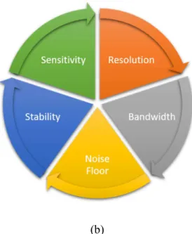
Other acknowledged characteristics of weakly-coupled resonating devices are linearity (attributed to high sensitivity [19], invulnerability against responding to ambient pressure and or temperature (i.e. common-mode rejection), [20]. These characteristics make these devices efficacious and hence being pursued over conventional method based on sensing the frequency variation of a single resonating device. In this context, one of the primary motivation of this thesis is to investigate the most fundamental and central performance parameters of coupled resonators such as sensitivity, resolution, noise, etc as depicted in Figure 1.2 (b).
(b)
Figure 1.2 (a) A schematic representation of two identical mass-spring-damper system coupled by spring to illustrate transduction principle, (b) graphic showing key performance parameters pertaining to new class of resonant sensor based on mode-localization.
1.1.4 Potential applications for mode-localized sensors
Figure 1.3 shows a graphic to indicate potential sensing applications that can be developed with coupled resonators utilizing the concept of mode-localization. These applications are discussed as follows: (refer also Figure 1.2 (a))
A displacement sensor – During fabrication, a suspended proof mass can be realized and be placed adjacent to one of the resonator separated by a coupling gap. Transduction takes place when any displacement of this suspended proof mass modulates the coupling gap between proof mass and its adjacent resonator, thus altering the stiffness of that resonator causing system imbalance. [21].
A charge sensor (electrometer) - A separate input port can be used to apply different DC voltages to one of the resonator (across an electrostatic capacitive gap) implying the change in charge (δq) at this input port. This exerts an electrostatic force to the resonator thus altering the
stiffness of the resonator causing system imbalance [22].
A force sensor- An electrostatic tensile force to one of the resonator can be applied, hence modulating the stiffness of that resonator. This electrostatic force can be generated by creating the voltage difference between the resonators and its neighbouring electrode separated by a coupling gap [23].
Figure 1.3 A graphic showing potential sensing applications that can be developed using coupled resonators.
An acceleration sensor- Given the same architecture of coupled resonators as in Figure 1.2 (a), when acceleration acts on the proof mass/es, single/differential electrostatic stiffness perturbation/s will be applied to the weakly coupled resonators, leading to mode localization, and thus, mode shape changes. Therefore, acceleration can be sensed by measuring the change in amplitude (or amplitude ratio) based readout as mentioned in section 1.1.3 above [24]. A mass sensor- A multi-DoF structure can be utilized to detect a change in the amplitude ratio output metric as a function of mass change (due to addition of mass [16] or removal of mass [25]) in a chain of 1-dimensional coupled resonating sensor architecture. Coupled resonators in mass sensing applications offer advantage of single measurement/device for multiple analytes.
Other applications may also be listed such as-electric field [26], tilt [27–29], etc. It is to be noted that all of these applications, excluding coupled resonators as a mass sensor, essentially implies the effective stiffness change of one or both (via differential perturbation) resonator/s. Therefore, all these sensors falls under the category of ‘coupled resonators for stiffness change applications’.
1.1.5 Fabrication using the state-of-the-art laser micromachining
Electrostatic actuation and capacitive sensing are widely used principles in the micro-electro-mechanical system (MEMS) field. A variety of devices including gyroscopes, accelerometers, and resonators based on the principle of electrostatic actuation and capacitive sensing have been developed using existing silicon wafer lithography based processes [3,4]. One of the essential features of these devices is the requirement of forming micro-size gaps/trenches through the active device layer, thus forming parallel-plate capacitors.
Conventional MEMS fabrication processes, such as surface and bulk micromachining, offer the advantage of large area patterning to create batch-processed miniaturized devices with sub-micron level resolution [30,31]. These processes, however, require expensive clean-room facilities. A relatively high number of fabrication steps are involved starting with photo-mask preparation, followed by several cycles of lithography, deposition, selective etching and finally wafer dicing [32,33].
For the first time, we show that a laser micro-milling technique can be utilized to machine micro-size kerf-widths, (referred as a capacitive gap in MEMS) to perform electrostatic actuation and capacitive sensing. We demonstrate that laser micro machining could be used as a pathway towards developing a diverse range of structures and devices. Moreover, it is suggested as a hypothesis that, some other micro-milling techniques [34,35] , if capable to form a micro-size cuts through a device thickness (thus providing a reasonable aspect ratio) could also be used. The benefit of using laser micromachining is the possibility to utilize new materials to enhance device performance [36]. At present, most of the laser-assisted work was used for making micro-cuts, drilling holes, engraving or forming embroidery onto a piece of a material [36–39], creating channels for microfluidic applications [40–42], and realizing micro-optical devices using photoresist [43]. A laser machining was used to develop an electro-mechanical based transducer and it experimentally demonstrated the possibility to use direct laser writing (DLW) to fabricate electro-mechanical based actuators and sensors with high precision and resolution. This fabrication method as proposed here can be particularly useful when there is no cleanroom access and there is a requirement for quick prototyping with materials other than silicon. This can potentially also be extended for small or medium-scale series production.
Given the novel fabrication platform (laser micromachining) as proposed in this thesis, it is worth investigating the performance parameters pertaining to the coupled resonator sensors. These performance parameters are sensitivity (in both open and closed loop), resolution (lowest possible detection limit), effective noise floor, etc.
By doing so, objective is to explore whether and how our proposed design offers any performance benefit over the coupled resonator sensors realized using MEMS technology. In this thesis, the possibility to fabricate such devices using state-of-the-art laser micro-machining/milling is also explored. Particularly, a goal is to fabricate a coupled resonator architecture and (as mentioned in the previous section above) evaluate its performance for stiffness sensing applications.
1.2 Thesis organization
Chapter 2 provides a first principle of MEMS resonator. An in-depth, including most recent literature coverage relevant to ultra-sensitive coupled resonators in sensing application is provided.
Chapter 3 provides a theory of operation of mode-localized weakly coupled resonators. This background was used to design and fabricate (using laser micromachining) our macro-scale two degree-of-freedom (DoF) coupled resonators for stiffness sensing applications. We develop a theory model to estimate a device sensitivity. We also analyse performance of our design for various operating conditions. A model developed using COMSOL Multiphysics software is also given in this chapter.
Chapter 4 presents system level models for coupled resonators built using a SIMULINK. A simulation results for variety of operating conditions are provided. We derive and compare the theoretical and simulated results of device sensitivity. We estimate the theoretical noise floor of our design and, subsequently determine the minimum resolvable shifts in to the output. We therefore determine a resolution for our macro-scale two DoF coupled system. We compare results of our theoretical model and system-level simulation and report a good agreement between them.
Chapter 5 begins with overview of various potential micromachining high-tech methods. It presents a laser micromachining fabrication and assembly processes. Fabrication outcome at the University of Liege and with the outside manufacturing service is compared and discussed in detail. We demonstrate a micro-size capacitive gap fabrication into metal parts of up to 2 mm thickness, thus resulting a high aspect ratio structure. This is useful in terms of MEMS transduction in capacitive devices and fabricating such deep trenches using laser micromachining to develop a transducer and/or sensor is unprecedented.
Chapter 6 presents initial experiments and measurement results for the developed prototype. Chapter 7 offers a platform for discussion and conclusion and future direction.
Appendix for the MATLAB script, circuit schematic, vacuum chamber used, etc. is presented at the end of this thesis.
Chapter 2
2 Literature Review
This chapter starts by reviewing the fundamentals of electromechanical transduction. A model for electrostatic actuation and capacitive sensing is given. Next, a theory for a resonator is formulated using a one degree of freedom mass-spring-damper model, transfer function analysis and electrical equivalent circuit model. Following this, an in-depth overview for ultra-precise weakly coupled resonators as sensors is presented.
2.1 Electrostatic actuation and capacitive sensing
Electrostatic actuation and capacitive sensing are widely used principles in the micro-electro-mechanical system (MEMS) field. A variety of devices including gyroscopes, accelerometers, and resonators based on the principle of electrostatic actuation and capacitive sensing have been developed using existing silicon wafer lithography based processes [3,4]. One of the essential features of these devices is the requirement of forming micro-size gaps/trenches through the active device layer, thus forming parallel-plate capacitors.
Figure 2.1 shows a schematic representation of an electrostatic actuation and capacitive sensing principle. It is one of the widely used principle amongst the devices for their operation. In resonator featuring electrostatic actuation and capacitive sensing, the electrical load and the mechanical restoring force govern the behaviour of a mechanical vibrating structure. The electrical load is composed of a DC polarization voltage, Vdc and an AC voltage vac. The DC
component exerts an electrostatic force on the mechanical structure, thereby deflecting it to a new equilibrium position, while the AC component vibrates the structure around this equilibrium position.
The combined electrical load has an upper limit beyond which the mechanical restoring force can no longer resist its opposing force, thereby leading to the structural instability called as ‘pull-in’, and the hazardous voltage associated with it is called ‘pull-in voltage’.
In a parallel plate actuator, a nominal capacitance is given as C0 A d
where ε, A, and d are permittivity, nominal electrode area and nominal capacitive air gap used for electromechanical transduction. As shown in Figure 2.1, when the top movable plate moves by a distance x, a net capacitance is given byC A
d x
. A total energy stored in the parallel-plate capacitor is given
by
1
22
E
CV
, where V is the potential applied across the capacitor plates. In case of a resonator, V=Vdc+vac. Therefore,
2 2 2 1 2 1 2 2 ac dc ac dc ac dc E C v V C v V v V (2.1)An associated net electrostatic force is therefore calculated as
2 2 2 2 2 2 2 2 2 1 2 1 2 1 2 1 2 1 2 2 ac dc ac dc ac dc E F CV x x A V x d x A V d x A v V d x A v V v V d x (2.2)Thus, we have components of this force at three frequencies: a force at DC, force at the excitation frequency f due to the term 2vacVdc and force at twice the excitation frequency due
to square term 2 ac
v . A force F at the excitation frequency is given by
2 2 1 2 2 ac dc ac dc A F v V d x A v V d x (2.3)Assuming displacement of a proof mass , x is relatively very small in comparison to nominal air gap, d i.e.,
x d
, equation (2.3) takes the form as
2 ac dc acA
F
v V
d
V
(2.4)A parameter, η is defined as the electrostatic transduction factor given by 0 2 dc dc dc C A C V V V d x d . A term C x
is called as a capacitive gradient. It is seen from above derivation that designing a large value of a nominal capacitance should benefit in enhancing a transduction factor, η.
2.2 Motional current
A charge voltage relationship in a capacitor is given by Q=CV. A current through the capacitor is given as 0 ac dc Q CV V C i C V t t t t V C C V t t (2.5)
The second term in equation (2.5) is given asVdc C Vdc C x x
t x t t . Equation (2.5) can therefore be written as 0 0 ac ac V x i C t t x j C V t
(2.6) The first term in the above equation is the ac or more commonly called feedthrough current and second term is called the motional current.2.3 A mass-spring-damper system
Figure 2.2 shows a model for a typical one degree of freedom (DoF) mass-spring-damper system. An expression of a force can be written asFe Ma M 22x
t , where 2 2 x a x t is an acceleration, v x x t
is the velocity and
x
is the displacement from its equilibrium position. Summing the forces, one can write2 2 e C S F F F F x x M C Kx t t
(2.7) Here, Fe is externally applied net electrostatic force, FS is the restoring force of the spring,which often tries to balance a net externally applied force, and FC is the force by the damper.
For a static case (i.e.,
x
is independent of time), FS = Kx. For a parallel-plate capacitiveactuation,
eff
S eff
F K x where, Keff = Km+Ke is effective spring constant, Km is mechanical
Figure 2.2 A mass-spring-damper system.
spring constant and Ke is electrical spring constant derived as (referring to equation (2.2))
2 2 2 2 2 3 1 e e F A K V x d x AV x d x A V d x
(2.8)Note that Ke has a negative effective value and therefore it causes a spring softening (decreasing
the effective value) as illustrated in Figure 2.1. Assuming that displacement x of a proof mass M is relatively very small than that of original capacitive gap, d (i.e. x << d), Ke can be
approximated as 2 3 e A K V d
and (V = vac+Vdc) for resonator.
For a linear, dynamic case where x is a time dependent, an expression for an effective restoring force can be written as
(t)
(t)
eff
S eff
F
K x
. An expression forK
eff can be derived aseff eff S S eff
F
F
x
K
t
x
t
.2.4 Transfer function for one DoF system
From Figure 2.2, a governing equation of motion for a single Degree of Freedom (DoF) mass-spring-damper system can be given as [44]
Mx Cx Kx F (2.9)
2 2 ( ) 1 (s) 1 X s F Ms Cs K M C K s s M M (2.10) where, 2 n K M
is the undamped natural frequency, and,
2 n 2
C K
M
M (2.11)where, is the amount of proportional damping, typically stated as percentage of critical damping,
C
cr (C
cr
2
KM
is the critical damping value). Equation (2.11) can also be writtenas 2 2
2 cr
C C K C K
M C M KM M . With this, equation (2.10) can further be written as:
2 2 1 ( ) (s) 2 n n X s M F s
s
(2.12) By using s j, we get, 2 2 2 2 2 2 2 2 1 ( ) ( ) 2 ( ) 1 2 ( ) 1 1 1 2 n n n n n n X j M F j j M j M j (2.13)Equation (2.13) shows how ratio
( )
( )
X j
F j
varies as a function of frequency
. This ratio beinga complex number has properties at different values of the ratio
n
.2 1 ( ) 1 ( ) n X j M F j K
(2.14)Magnitude and phase are expressed as ( ) 1; ( ) 0
( ) ( )
X j X j
F j K F j
(Phase is zero as the sign is
positive)
Case 2) at high frequencies,
2
n
n22
( )
1
( )
X j
F j
M
(2.15)Magnitude and phase are expressed as ( )
( ) X j F j 2 1 M and 0
(
)
180
(
)
X j
F j
respectively.(Phase is 1800as the sign is negative)
Figure 2.3 Magnitude-frequency response of a single DoF mass spring damper system [44] Case 3) at Resonance,
n 2 1 ( ) ( ) 2 n 2 j X j M K F j j
(2.16)Magnitude and phase are expressed as ( ) 1
( ) 2 X j F j K and 0
(
)
90
(
)
X j
F j
respectively. AtFor 1, system is underdamped. This means energy dissipation is sufficiently small so that free-vibration response of the system is oscillatory. This is the case with most MEMS resonators. The free-vibration response of an underdamped one degree of freedom (DoF) system takes the form as
0t
cos
sin
d d
x t
e
A
t B
t
(2.17)Where, A and B are constants that depend on the initial values of x(0)and x(0)that set the system into free vibration and ωd is the damped natural frequency given as d 0 12 . For a damping ratio, 0.2 d 0
K M
where ω0 is the undamped natural frequency asstated earlier. Since
2
C
KM
, a quality factor for a resonator is given as 12 KM Q C .
Figure 2.3 shows a magnitude-frequency response of a system.
2.5 Coupled resonators
Using an array of resonators for frequency and timing application has been quite well known in the MEMS field. An array of mechanically coupled structures have been proposed for increasing the transmission gain of the signal [45], for oscillator application [7], etc.. In [46], two microscale clamped-clamped beams were mechanically coupled by a soft flexural-mode mechanical spring and demonstrated its usage for filtering application. A study [47] presents coupling techniques for implementation of high order narrow-bandwidth bandpass filters from micromechanical resonators using electrical coupling elements. Active and passive coupling elements were used in this work to implement high order resonant systems from individual MEMS resonators. The concept of passive coupling of resonators used capacitors as the coupling elements for filter synthesis. Active coupling of resonators used transistor-based amplifying circuits. In a more recent study [48], A CMOS-MEMS fabrication platform was used to implement a mechanically coupled array of free-free beams resonators and filter application was demonstrated [43].
2.6 Coupled resonators in sensing applications
Since last decade, in the MEMS community, there has been a paradigm shift in the research referring to MEMS resonating sensors being developed for variety of sensing applications. Specifically, a widespread interest has aroused using 1-d chain of a coupled resonating proof masses, more familiarly refereed as weakly coupled resonator sensors [16,17]. These sensors attribute an ultra-high sensitivity [17,18] manifested via novel transduction principle, i.e. sensing magnitude of vibrational energy exchange between the moving proof masses subject to a small disruption introduced into the system which alters either an effective mass, ∆m or an effective mechanical stiffness, ∆k of one of the proof mass element in a chain. In coupled resonating sensor devices, a coupling between the proof masses is constituted either electrostatically or mechanically. Such sensors are also characterized by a veering point or loci which is described as a reference point from where eigenvalues and/or eigenvectors of this coupled system abruptly change and move away from each other (eigenvalues do not cross one another but eigenvectors do) subject to a small disorder injected into the system. This change
in eigenvalues and/or eigenvectors is larger and linear to some extent as the magnitude of an applied disorder is further increased. Veering point thus is also used to describe the amount of spacial energy re-distribution amongst the vibrating proof masses in a chain when there is a disorder present into the otherwise originally balanced system. If this reference veering point/loci is at the centre, it is regarded as an inherent symmetric system. Ideally, this condition should occur when ∆k or ∆m is zero, i.e. without the introduction of any disruption into the system. However, owing to the manufacturing tolerances, ideal symmetric system does not exist into the practice and individual devices coupled together as a whole system exhibit mismatch in the geometric features [49]. Unequal energy distribution is also a result of choice of driving scheme used for operation and it has recently been shown in [50] that in-phase mode, simultaneous driving of both the proof masses resulted in symmetric veering point for the eigenvalues of the system. However, the veering loci of eigenvectors was observed to be shifted away from the symmetry. In such situation, by introducing an external disruption into the system, equal energy distribution between vibrating
Figure 2.4 Ultrasensitive mass sensor using a mode localization in coupled microcantilevers [16]
proof masses was achieved and the point/loci at which this happened was refereed as revived veering point of the system. This act could be viewed similar to a calibration scheme for any sensor wherein a sensible measurement can be done and therefore accuracy in the measured physical quantity can be assured. Away form this veering point, magnitude of energy exchange between proof masses resonating in a particular mode was measured and thereby device sensitivity and linear measurement range could be determined. Potential applications of coupled resonator sensors are classified as mass detection and identification [51], force sensor, electrometer (electrical charge measurement), displacement sensor, and acceleration sensor, to name a few.
Spletzer et al., [16] proposed for the first time that a vibration mode localization can be used for sensing purpose. This is shown in Figure 2.4. Two mechanically coupled cantilevers were used that experimentally demonstrated about two orders of higher in magnitude relative changes into the eigenstates (5% to 7%) than relative changes in frequencies (0.01%).
Following this, a study in which an array of four microbeam sensors (cantilevers) were used for the detection and identification of multiple analytes [52]. It is shown in Figure 2.5 below. A single output signal was measured optically from the shuttle mass, using a laser vibrometer, to determine the resonance frequencies M1–M4, which correspond to the localized microbeam
modes of the coupled system.
Figure 2.5 A microbeam sensors utilizing mode-localization to detect and identify the analyte [52]
In the work reported by Thiruvenkatanathan et al,[17], authors used two different types of MEMS structures namely free-free beam and double-ended tuning fork as shown in Figure 2.6. An electrical coupling as opposed to the mechanical coupling was used and about two orders of high sensitivity to eigenstate shifts was demonstrated. In the same study, an effect of initial mechanical asymmetry was also investigated. Amplitude change instead of a frequency change as a sensor output was proposed. A maximum percentage change in eigenstates and resonant frequency shift of about 8.9% and 0.019% respectively were reported. Same group also showed a mode-localized MEMS electrometer [22] with the double-ended tuning fork resonator topology and also a mode-localized displacement sensor [21]. Reported shifts in eigenstates
(a) (b)
(c)
Figure 2.6 Electrically coupled weakly coupled resonators with enhanced sensitivity (a) A fabricated double-ended tuning fork and (b) two free-free beam resonators and (c) a
representative two DoF coupled resonator model [17]
were about three orders of magnitude higher than resonant frequency variations. Equal but of opposite polarity DC voltage difference was applied on the two resonators, which are coupled by an electrostatic spring. Note that Km1 = Km2 = Km, ke1 = ke2 = ke, keff = km-ke, this put the system
under initial symmetry and at the same time established a coupling spring, Kc between the two
resonators. Later, the DC voltage on one of the resonators was varied thereby altering the effective stiffness of that particular resonator (electrostatic spring-softening effect) to introduce a disorder, ∆k = keff1- keff2. (In initially established symmetry of the system keff1 ≈ keff2 , ∆k = 0).
The approximation sign denotes an initial asymmetry due to fabrication tolerances). By decreasing the DC voltage on one of the resonator also alters a coupling spring, Kc and it was
called as a way to tune the mode shape sensitivity of the system under test.
This action as mentioned above also decreased the effective value of Kc, making it weaker. For
c
k K
sensitivity to mode shape changes, i.e. shifts in eigenstates were reliably measured. In short, with such biasing schemes as reported in this research, Kc is also changing (thus
parametric sensitivity) for a given stiffness imbalance between the resonators which, in real systems is undesirable as usually Kc has to be fixed to reliably measure the impact of ∆k, as an
external disturbances into the system.
It was proposed that mode shape sensitivity could be enhanced either by increasing the magnitude of externally added perturbation and/or by simply altering (decreasing) the coupling spring, Kc between the two resonators. It is also noteworthy that by decreasing Kc could
increase the mode shape sensitivity of the system under investigation but it remains ‘insensitive to the variations in the resonant signal frequency shifts. In other words, frequency sensitivity to the varying coupling strength is ideally zero.
Zhao et al., [18,23,53] demonstrated a highest possible amplitude ratio based sensitivity of amplitude ratio to stiffness perturbation (about 13558) with the coupled resonators employing an array of three adjacent resonators. A prototype fabricated by this research group is shown in Figure 2.7. Same group also reported a force sensor [23] with a sensitivity of about 4.9×10⁶/N. A concept of bias
![Figure 2.5 A microbeam sensors utilizing mode-localization to detect and identify the analyte [52]](https://thumb-eu.123doks.com/thumbv2/123doknet/6512261.174546/38.918.261.656.242.610/figure-microbeam-sensors-utilizing-localization-detect-identify-analyte.webp)
![Figure 2.7 A coupled resonator sensor employing an array of three resonators [18]](https://thumb-eu.123doks.com/thumbv2/123doknet/6512261.174546/40.918.193.759.478.797/figure-coupled-resonator-sensor-employing-array-resonators.webp)