HAL Id: hal-02135683
https://hal.archives-ouvertes.fr/hal-02135683
Submitted on 21 May 2019
HAL is a multi-disciplinary open access
archive for the deposit and dissemination of
sci-entific research documents, whether they are
pub-lished or not. The documents may come from
teaching and research institutions in France or
abroad, or from public or private research centers.
L’archive ouverte pluridisciplinaire HAL, est
destinée au dépôt et à la diffusion de documents
scientifiques de niveau recherche, publiés ou non,
émanant des établissements d’enseignement et de
recherche français ou étrangers, des laboratoires
publics ou privés.
Synthesis of T-Nb2O5 thin-films deposited by atomic
layer deposition for miniaturized electrochemical energy
storage devices
Saliha Ouendi, Cassandra Arico, Florent Blanchard, Jean-Louis Codron,
Xavier Wallart, Pierre-Louis Taberna, Pascal Roussel, Laurent Clavier,
Patrice Simon, Christophe Lethien
To cite this version:
Saliha Ouendi, Cassandra Arico, Florent Blanchard, Jean-Louis Codron, Xavier Wallart, et al..
Synthesis of T-Nb2O5 thin-films deposited by atomic layer deposition for miniaturized
electro-chemical energy storage devices.
Energy Storage Materials, Elsevier, 2019, 16, pp.581-588.
�10.1016/j.ensm.2018.08.022�. �hal-02135683�
OATAO
O
pen
A
rchive
T
oulouse
A
rchive
O
uverte
(OATAO)
OATAO is an open access repository that collects the work of some Toulouse
researchers and makes it freely available over the web where possible.
This is
version published in:
Official URL:
To cite this version:
Any correspondence concerning this service should be sent to the repository administrator:
Synthesis of T-Nb
2
O
5
thin-
films deposited by Atomic Layer Deposition for
miniaturized electrochemical energy storage devices
Saliha Ouendi
a,b, Cassandra Arico
a,b,d, Florent Blanchard
c, Jean-Louis Codron
a, Xavier Wallart
a,
Pierre Louis Taberna
b,d, Pascal Roussel
c, Laurent Clavier
a, Patrice Simon
b,d,⁎,
Christophe Lethien
a,b,⁎aUniv. Lille, CNRS, Centrale Lille, ISEN, Univ. Valenciennes, UMR 8520 - IEMN, F-59000 Lille, France
bRéseau sur le Stockage Electrochimique de l’Energie, CNRS FR 3459, 33 rue Saint Leu, 80039 Amiens Cedex, France
cUnité de Catalyse et de Chimie du Solide (UCCS), Université de Lille, CNRS, Centrale Lille, ENSCL, Université d’Artois, UMR 8181 UCCS, F-59000 Lille, France
dCentre Interuniversitaire de Recherche et d'Ingénierie des Matériaux (CIRIMAT), CNRS UMR 5085 Université Paul Sabatier, 118 route de Narbonne, 31062 Toulouse, France
Keywords:
Atomic Layer Deposition Nb2O5
Micro-devices Surface capacity
A B S T R A C T
Atomic Layer Deposition has been used to grow 30 to 90 nm thick amorphous Nb2O5films onto Pt current collectors deposited on Si wafer. While T Nb2O5polymorph is obtained by further annealing at 750 °C, thefilm thickness and the resulting electrode areal capacity are successfully controlled by tuning the number of ALD cycles. The electrochemical analysis reveals a lithium ion intercalation redox mechanism in the T Nb2O5 electrode. An electrode areal capacity of 8 μAh cm ² could be achieved at 1 C, with only 40% capacity loss at 30 C (2 minutes discharging time). This paper aims at demonstrating the use of Atomic Layer Deposition method in the fabrication of Nb205based on chip micro devices for Internet of Things (IoT) applications.
1. Introduction
Li ion micro batteries
[1 3]
(MB) and micro supercapacitors
[4 10]
(MSC) are two complementary electrochemical energy storage
(EES) miniaturized systems. While MB o
ffers high energy and lower
power densities, MSC are particularly attractive for applications where
high power is needed but su
ffer from limited energy density. Charge
storage processes occurring in MB and MSC are totally di
fferent in
nature leading to complementary properties. MSC based on ion
adsorption/desorption in carbon porous electrodes
[8,11,12]
o
ffer
great cyclability and high power densities; such miniaturized EES are
characterized by rectangular shape cyclic voltammograms and linear
galvanostatic charge discharge profiles. Similar features are observed
with MSC based on pseudocapacitive materials
[6,7,13]
where fast
redox surface reactions are responsible for the continuous change of
oxidation state of the electrode material
[14,15]
, without any phase
change during cycling. Di
fferently, faradic reactions taking place in the
bulk of active materials lead to redox peaks and
flat plateaus are
observed during voltammetry and constant current charge discharge
experiments, respectively. Such charge storage process is often accom
panied by a phase transformation of the electrode material (LiCoO
2,
LiMn
2O
4, LiFePO
4, LiMn
1.5Ni
0.5O
4, TiO
2…) depending also of the
particle size
[16 18]
. In such materials, the control of the crystal
lographic structure and the ionic diffusion paths is of major importance
to achieve improved electrochemical performance.
Among the large variety of electrode materials exhibiting high
energy and high power densities, Nb
2O
5has been identified as a
promising candidate for Li ion batteries. Several polymorphic forms of
Nb
2O
5are described in the literature, such as TT Nb
2O
5(pseudohex
agonal), T Nb
2O
5(orthorhombic), M Nb
2O
5(tetragonal) or H Nb
2O
5(monoclinic)
[19,20]
. Low temperature forms (TT Nb
2O
5and T
Nb
2O
5) have been deeply investigated
[21 26]
by B. Dunn et al., owing
to the fast lithium ions intercalation process occurring in the bulk
material. Particle size (nanoscale), porosity and electrode formulation
are
finely tuned to produce high mass loading electrodes where the
charge storage process is not limited by ion di
ffusion, thus leading to
the concept of Li ion pseudo intercalation reaction
[25]
. Electron
transport is signi
ficantly improved in these materials by the addition
of a highly conductive agent/sca
ffold in the composite electrode such as
graphene, carbide derived carbon or carbon black
[23 26]
to tackle the
low electronic conductivity of the Nb
2O
5material (3 × 10
−6S cm
−1at
300 K). However, the cost as well as the limited available Nb resource
⁎Corresponding authors at: Réseau sur le Stockage Electrochimique de l’Energie, CNRS FR 3459, 33 rue Saint Leu, 80039 Amiens Cedex, France E-mail addresses:simon@chimie.ups-tlse.fr(P. Simon),christophe.lethien@univ-lille.fr(C. Lethien).
~
M•@ifijilUMNiiMiiihW A
@l#MIIM&Eil4911:il
Sdf,Jill\lttrg ~tttdi.ol Nb(OEt~j!j
l"C(!Chcftq
t
l!J
~C'\lr"SOI'... , .... ,
~ '/5J
·
tl
,
0
,
.
~
-
~
....
.,
~-
.:=
pt Tdepo54tlon~
230-33o
•
c
Nb10s thln ftlm on SI/At10, / Pt stacked layers
1
1
/.
"i ;;-.,_
i
t
-·
n
-·
-
1
-
~
.
l
i
i
,
1
Time
(s):
'----y---'!
1 lALDcyde 750* C- 2 h under air atmMMFl:Nfii
·
i!IIM&itdl
IFl&Mi&ih:iéiifi:I1
a) 0,08~ - - - ~
ü
{Ï' 0,07·
+
.
a,
o
,
os
~ - - - ~
i
0,07Si
/
A
l
20
3/
Pt
/
Nb
20
5m
o,os
~ - - - ~
-og,
0,07 --~- 0,06 ····• ....-
·,
+
+
.s
E
o,os
'
+
·
···
·
-;,
++•+•
•
-
·
·+
··
·
·
·
·
·
···
·
·
*
··
·
·
·
·
·
···
···
···
·
··
E
o,os
.s
.
+
····
·
+
:
:::
+
'
'
::•
f
: .
.
+
··
·
·
·
···
+
····
i
0,05 .... : ....·
·
·
·
···
·+
· ···-···
·· +
(S
0,04+
Gl 0.06~
t) 0.04...
8_
0,03 Nb(OEl)s : 2 s / 6 s / 150 socmlii
a. 0,03..c H2O : 3 s / 6 s / 100 sccm <:: 0,02
t
6.,
+
tpu,ge =6s2so·c
H2O. 38 /6 si 100 sccm 1000 cycles G> 0,05Ô'
0,04...
:g_
0,032so
·c
Nb(OEt)5: 2 s / 6 s / 150 sccm2
...
= s 1000 cycles~~~~ ~
uo
uo
~o
~o
Temperature
deposition (°C)
1
0,02 ~ 0•01 ~ ~ - ~2- -3~ - ~4~ - ~5- ~6 3401
0,02 t..,._ = 6 s 1000 cycles ~ 0,01 O 2 3 4ôt
Nb(OEt)5
(s)
ôt
H2O
(s)
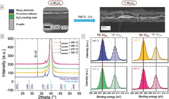
Ftg. 1. A Scl>ematic ci the T-Nb,05 thin films deposited on silioon roated AJ2O ~ stacked layers by ALD.
The
c,ystalline structure of the T-~O5 bighlights the layered arrangement between the 6 or 7 02 (in yellow) and the Nb5• niobium ions inside the polybedra. B. Descriptionci
the two step proeess used to form the T-Nb:,O5 ortborbombic structure: an amorpbous layer(a-Nh2Qs) i<; deposited by AID and the film is annealed at 750 °C during 2 b under air atmospbere to reacb the formation
ci
the T-Nb:,O5 polymorph. C. Growth per cycle of the a-Nh2Q5 layer as a function of the deposition temperature inside the ALD reactor, ag determined for 1000 cycles ofNb(OEt)5 (2s)/purge (6s)/Ha0 (3s)/purge (6s). D. Growth per cycle of the a-Nh2Q5 vs the Nb(OEt)s and E. the water pulse durations. Pul<ie du rations for water, Nb(OEt)s and purge step are 6xed to 3 s, 2 s and 6s, respectively. The temperature of the silioon substrate is set to 250°C. (For interpretation of the referenœs to oolor in this figure legend, the reader i<;referred
to the web version of this article).currently limit the development of
Nb
based negative electrodes for
large size
li
ion battecy applications
.
However,
this does
not
apply to
micro
devkes
thanks to the small amount of materials used.
There
is
then
intere.sting opportunities for
designing
thin
films of
Nb:!O
5for
micro
devices
applications.
Thin
film electrode for
MB
[27,28]
or MSC
[5,11)
applications can be prepared
by
using magnetron sputtering
technique or, alternatively, by Atomic Layer
Deposition
(ALD)
which
has also been found as a suitable deposition tool, compatible with
CMOS
facilities, to grow
thin
films
on
large
scale substrate with
high
uniformity and
homogeneity
[29 35)
.
In this paper,
ALD
technique has been
used
to grow highly adhesive
30 to 90 nm thick Nb:z•s films onto
Pt
current collectors
deposited
on
Si wafer, and further
characterized
as negative
electrode
for
Li
ion
micro battery applications
.
The
first part of
the
study focuses onto
the
synthesis process and the structural characterizations of
T
Nb:z•s thin
films. Then, electrochemical characterizations
of Nb:!O
5thin films have
been achieved, showing
the
typical signature of
Li
ion intercalation
reaction with redox activity present in the 1 2 V vs
Ref
potential range.
Interestingly, although
dense
and conducting additive
free
Nb:!O
5films
where
prepared, these films could
deliver up
to 8 µAh
cm-
2at
l0mvs
-
1•This
paper a
i
ms at
demonstrating
the suitable growth of
Nb:!Os thin films by
ALD
acting as an attractive negative electrode for
micro
devices
applications
.
2.
Experimental
section
2
.1.
Film preparation
Prior to Nb:!Os deposition, 3 inch silicon wafer
is
coated with
Al203
(H)0 nm) and Pt (50 nm)
layers
to be used as a current collector, using
a
Beneq TF$
200
ALD
reactor
.
Al2•3
layer
is used to prevent the
interdiffusion
between
Pt and Si when
the
stacked
layers
are annealed
[27]
. Nb:!Os
thin films are grown in a Picosun R200
ALD
reactor un
der
an Ar gas pressure around
0.5
mbar. Argon
is
used as the carrier and
purging gas.
Niobium(V) ethoxide
Nb(OEt)
5and deuterated water are
used
respectively as niobium precursor and oxygen reactant.
Nb(OEt)
5precursor was purchased from Strem Chemicals (claimed purity 98%).
The
sublimation temperature is 185 °C for the niobium source while
the water source is kept at
room
temperature
.
The
reactor temperature
is tuned from 220
up
to 330 °C. A total of
1,000
deposition
cycles were
achieved to study the
evolution
of
the
Nb:z•s growth per
c
ycle rate
(GPC) as a function of the
deposition
temperature
.
Nb(OEt)s and water
are pulsed into
the
chamber alternatively
with
different
pulse time
duration
separated by 6 s argon purge; the
whole
process accounts for
one deposition cycle.
The number
of cycles is progressively increased to
reach the targeted
thickness. The
as
deposited
Nb.iO
5thin
films
are
amorphous and noted as a Nb:!O
5layer.
The
transformation from a
Nb:!O
5to
ccystallized,
orthorhombic
T
Nb:!O
5polymorph
was
achieved
by
thermal
annealing at 750
"C
during
2
h
under air atmosphere of the
films.
The
resulting stacked
layers
are noted as Si /
Al
20:i /
Pt/
Nb:!O
5 •2
.
2. Sample morphological and structural characterization
Thickness
of a Nb:!O
5thin
films
was detennined by
X
ray reflectiv
ity
(XRR)
fits
on silicon substrate.
The
film morphology of
Al
2O
3/Pt/
Nb:!O
5stacked
layers
was assessed
by
SEM (Zeiss Ultra 55 Scanning
Electron Microscope).
Crystallographic orientation and phase identifi
cation were
detennined
by specular X ray diffraction
w
28 scans
(XRD, Rigaku SMARTLAB multi purpose six axis diffractometer
9kW
rotating anode) using CuKa radiation
(À=
1.5418Â). The
Pt current collector
Al,O, insulting layer
~
Nb20 5 electrode 750 •c-2 h SI waterŒI
5 0 0 - - - ~ ~ - ~ ~
l9
400
-
::s
~300
>-~
c:
200
J.... _ _ _ _ ....__,-:"/l_s
C:100
-0
T ~!,pl POF 30-0873 pt P()f 06-0802"
~20-
el!
iî
__
,,_
â_
;.
8
~;,: ~~-100J...:J.~...;:.~~...,..::..u..:::...J,..._...,:..
LC;....
--r'-~-I
25
30
35
40
45
50
55
2theta (
0 )...,.
::, ~f
J!! .5 Nb 3d512 Nb 3d312 205 208 '207 208 209 210 211 212 213 206 208 '207 208 209 210 211 212 213Blndlng energy (eV) Blndlng energy (eV)
Fig. 2. A Scanning Electron Microooope (SEM) images (cross-sections)
ci
the AI.03'Pt/Nb.Os stacked Jayers on silicon wafer: œ-deposited thin films (top~ are annealed at7~•c
under air atrnosphere (bottom, tilted view).The
pulse conditions of the Nb precursor and the water reactant correspond to the optimizoo parameters reported tn Fig. 1. The d_epooruon ternperature is 6xed at 250 °C and 1,000 ALD cycles are done to prepare - SOnm-thick fihns. B. X-Ray Diffraction analysis of Nb.Os thin films (annealed at 750 °C) as a functton of the depœition ternperature, from 250 up to 300 °C. AD the films were annealed at 750 °C to form T-Nb.05 orthorhcmbic structure (pdf 30 0873). C. X-ray Photoelectron Spectroooopy analysis (XPS) of the corresponding annealed thin films vs the depooition ternperature, showing Nb 3d core levels.oxidation state of the niobium element was measured
by
X Ray
Photoelectron Spectroscopy using a Physical Electronics type 5600
equipment.
2.3. Electrochemical analyses
Electrochemical measurements were conducted in home made fiat
cells operated in an Ar filled glove box. Cells are assembled using the
AhOs/Pt/Nb:!Üs stacked layers as working electrode while pure li
served as counter and reference electrode. A mixture of 1 M LiClO4
dissolved in Ethyl Carbonate (EC)/Dimethyl Carbonate (DMC) (1:1)
was
used
as electrolyte. Galvanostatic cycling and cyclic voltampero
metry were performed with a Biologie VMP3 potentiostat/galvanostat.
3.
Results and discussion
The preparation of
T
Nb:!O
5films is shown in
Fig.
1.
A schematic
describing the stacked layers is depicted in
Fig.
lA
.
a Nb:!Os thin films
were deposited from ALD onto 50 nm thick Pt current collectors. A
layer of Al2O
3(100 nm) was
used
as a barrier diffusion layer at the Pt/
Si wafer interface. The transformation from a N ~
5to crystallized
orthorhombic
T
Nl>.!Os polymorph was achieved by thermal annealing
at 750
°C
during 2 h under air atmosphere. During the annealing
process, the presence of the Al2Üs thin
film
avoids interdiffusion
between Si and
Pt
so that PtSi alloy cannot form
[27)
.
The crystal
structure of the
T
~Os is descnbed in
Fig.
1A
Each Niobium atoms
is localized at the center of edge or corner sharing distorted polyhedra
clustering 6 or 7 oxygen ions in the
ab
plane giving rise to the
formation of tilted octahedral (Nb0
6)or tilted pentagonal bipyramids
(Nb0
7)respectively. These polyhedra are connected by corner sharing
along the c axis. While the lithium intercalation process in
T
Nb:!Os is
known since the 1980s, recent
in situ/operando
experimental studies
[24,25,36)
and theoretical modelling lead on the
T
Nl>.!O
5have been
carried out to study the charge storage process due to the complexity of
the orthorhombic structure. On the one hand, experimental studies
have confirmed that lithium ion insertion in the crystal structure is
achieved
via
a solid solution mechanism (with no phase transition),
together with a contraction/expansion of the c axis lattice parameter
upon cycling. On the other hand, several computational studies clearly
show that the
(001) planes exhibit low energy barrier for Li ion
transport inside the orthorhombic structure
[37,38)
.
The synthesis
process ofT Nb:!Os thin films is schematically descnbed
in
Fig.
lB
.
The
growth conditions of the thin films by ALD are optimized to produce
amorphous Nl>.!Os layer on silicon coated Al2Os/Pt substrate. Post
annealing at 750
•c
in air atmosphere is then performed after the
deposition to form
T
Nb:!Üs- Nb(OEt)s precursor being liquid at room
temperature, the temperature should be close to 190 °C to promote the
liquid gas phase transformation. The self saturating nature of the
surface reactions occurring during each half cycles can be considered
as the main characteristic of an ALD process. Saturation curves were
investigated as a function of the exposure dose of precursors. The
growth per cycle (GPC) of Nb:!Os is shown vs the deposition tempera
ture (
Fig.
l
C), the time duration of the Nb precursor (
Fig.
ID
) and H2O
reactant (
Fig.
lE
). A constant a Nb:!Os growth rate of 0.05
±
0.005 nm/cycle is measured for deposition temperature between
250 to 330
•c,
which defines stabilized ALD deposition process. The
high GPC value of 0.07 nm per cycle achieved at temperature (230 °C)
is due to physisorption phenomena of the active species instead of the
self saturating chemisorption of exposed surface
[39)
.
The deposition
temperature has thus been fixed to 250 °C.
The GPC is investigated as function of the Nb(OEt)
5duration and
the water pulse duration respectively. A stabilization of the a N~s
growth rate around 0.05 nm per cycle is observed as soon as the pulse
time is higher
than
1.5 and 2.5 s for the Nb(OEt)
5precursor (
Fig.
ID
)
and H2O reactant (
Fig.
lE
), respectively. Such a saturation
in
the
deposition rate clearly confirms the self limiting film growth of the a
Nb:!O
5•The measured GPC is in agreement with the value reported by
other research groups
[40,41)
.
The as deposited Nb:!O
5layers are amorphous whatever the
selected deposition parameters. Consequently, the films have to be
annealed
in
order to crystallize in the orthorhombic structure.
Fig.
2A
shows a SEM cross section of the Al2Os/Pt/~Os staked
layers. The electrode structure has a dense morphology before and after
the annealing process at 750
°C
during 2 h under air atmosphere. After
annealing, the Nb:!Os layer shows the formation of large grains while a
smooth surface is observed before the annealing for the a Nb:!Os.
X Ray Diffraction analysis of the samples is
reported
as a function of
the deposition temperature in
Fig.
2
B. Ail samples show the (111)
diffraction peak of the
Pt
current collector observed at 28
=
40° (PDF
card
04
0802), whatever the deposition temperature. The (181) and
(201)
Bragg
peaks identified on the 4 samples
are
consistent with the
T
Nb:!Os orthorhombic structure (PDF card
30
0873). At
300 °C,
a
small
contnbution of the (001) diffraction
peak
is
observed at 28
=
22°
on the XRD pattern.
This
analysis confirms the preferential orientation
of the films.
XPS
core level analysis in the
region
of 0
700
eV were carried out
on these 4 samples. No etching is
done
on these samples before the
XPS
analysis.
The
survey scan and a focus on the O
1s
core level
are
reported in Fig.
SllA
while the
Nb
3d
level spectra is shown in
Fig.
2
C.
Only the
doublet
of the
Nb
3d
core level is detected at 207.5 eV and
210.5 eV, assigned to the
Nb
3ds12
and
Nb
3~/2
levels,
respectively
.
These
values
are
consistent with the presence of Nb
5+
[42,43]
for all
samples. Two main contributions at 530.6 eV and 532 eV are observed
on the O 1
s
spectra (Fig. SllB) which fits with binding energies
reported
[44,45]
for Nb:!Os.
To
clearly
demonstrate
the superior electrochemical behavior of
T
Nb:!O
5as compared to the amorphous a N~O
5,electrochemical
analysis is reported in Fig.
3
A and
B.
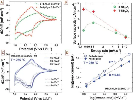
From the cyclic voltammograms
(CV)
at 0.5 mV s
-
1shown in Fig.
3
A, we observed on the one band no
clear redox
peak
of the a Nb:!O
5and a huge irreversible capacity when
cycled between
1
and
3
V vs
Li
/li
+
.
Redox peaks are highlighted
around 1.8 V vs
L
i/li
+
on the CV of the
T
Nb:!O
5•On the other band,
the
T
Nb:!Os thin
film delivers
a higher areal capacity than the a N~s
when the sweep
rate
is increased from
0.5
up to l0mvs
-
1(Fig.
3
B).
Such conclusions
are
classically observed
by
other
research
groups
[22,46]
. The
electrochemical characterization of the 50nm thick
Nb:!O
5film (1000
ALD
cycles) prepared at 250
°C
is shown in Fig.
3
C
and
D
at varions sweep rates. Cyclic voltammograms for sweep
rates
from
0.1
to 5mvs
-
1are similar to CVs of
TNl>:!0
5synthesized or
~
40 -~E
0 20u.:
-S
0w
"O--0
-20 "O -40 ~[g
30 -~E
15 0u.:
-S
0w
"O Ô-15 "O -30 - -a-Nb2O0 at0.5 mv
.
s
·•
- + -T-Nb,05 at 0.5mv
.
s·
•
1,0 1,5 2,0 2,5 3,0Potential
0/
vs
Li/L
n
1 M LiCIO, in EC/DMC : 1/1T = 250
•c
-
-
0
0
.
.
3mv.s·
Smv
.
s·'
'
-
0
.
7mV
.
s
"
1 ----1mV
.
s
'
1 -·-·-· 3mv
.
s
·
•
···5mV.s' 1,0 1,5 2,0 2,5 3,0Potential
(V
VSLi/Lt)
deposited by other
deposition
methods
[20,22,24]
. Broad
cathodic
peaks corresponding to
Lithium
intercalation are observed around 1.8
V vs
Li
/li
+
while the corresponding anodic
peak
can be seen at
1.
75
V
vs Li/Li
+
[20,22,24]
.
No redox activity is observed beyond 2.2 V vs
li/li+.
The
slight shift of the anodic peaks as well as the merging of the
two cathodic peaks when increasing potential scan rate shows a
dependence of the electrochemical kinetics with the scan
rate
.
Fig.
3
B
shows the plot of the peak current versus the scan rate in
logarithm scale.
Peak
current from CV experiments follows a power law
as shown in Eq.
1
:
(1)
where
"lpea1c"represents the peak current (mA) and
"v"
is the scan rate
(mvs
-
1).Ab value of
1
is calculated for the cathodic peaks, which
evidences a non diffusive charge storage mechanism, in the
T
N~O
5material within the potential scan rates range studied.
The
average b
value decreases to 0.83 when considering the anodic current, showing
the emergence of a diffusion limited process or ohmic limitation.
Although the dense structure of the film as well as the absence of any
conducting additive limit their power performance, those results
confirms the pseudocapacitive behavior of these
T
N~s thin films
prepared from
ALD
technique.
One important parameter for micro
devices
is the
area1
(surface)
capacity
(mAh
per cm
2 ),which
depends
on the film thickness deposited
onto the substrate.
The
growth
deposition
rate
of Nb:!O
5film from
ALD
bas been studied by tuning the number of
ALD
cycles.
The
change of
the
film
thickness (a Nb:!O
5)as a function of the number of
ALD
cycles
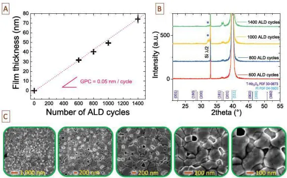
is shown in Fig.
4
A
The
linear change of the film thickness from 30 to
75
nm
validates the
deposition
temperature and the pulse sequence
previously selected
(Fi
g. 1
). After an annealing at
75
0
°C
of the
prepared a N~s films, the formation of
T
N~s is confirmed from
the presence of the two diffraction peaks ((181) and (201)) on the
XRD
patterns of the 4 samples.
The
intensity of these two peaks increases
-9
~---~
~E
~
8+·
·
·•
..
,
..
:+
~ a-Nb205+
T-Nb205 :::i.;1
'ü
CIi C. 6~
~
5
-ê
:::,··
...
...
-·
··
~
-
....··
.
.
~
en
4
0,4 0,6 0,8
+---~
1
2
4
6 8 10
@]
_
<(2,
1,6-
-
C~
1,2 :::, 0 ~ ~ 0,8 C.F
0.4Sweep
rate
(mv
.
s·
1)-
0-
·
Cathodlc peak-
+-
·
Anodic peakT = 250
•
c
1M LiCIO, in ECIDMC (1/1) -0,6 -0,3 0,0 0,3 0,6log(sweep rate)
(mv.s-
1)Fig. 3. A. Electrochemical analysis of the Nb,05 sample (1250 ALD cycles) deposited at 250 °C: cyclic voltammograms of the as-deposited Nb,O5 (a-Nb.Os) and annealed Nb,05 at
750 °C (f-Nb,Os) samples measured at 0.5 mV s 1• B. Evolution ci
the
surface capacity (in µAhcm2)
as a fonction of the sweep rate demonstrating the superior electrochemical behavior of the T-Nb,05 (1250 AID cycles). C. Cyclic voltammograms (CV) of the T-Nb,05 thin film deposited at 250 °C (1000 AID cycles) and tested in 1 M üCIO4 EC/DMC (1/1)organic electrolyte as a function of the sweep rate from 0.3 to 5 mV s 1• D. l>-value determination issued from the anodic and cathodic peak current vs sweep rate. From the CV, l>-value is
~
80
-
E
10
C'-"
60
en
en
Q)50
~
40
.
2
30
.c
-
20
E
1
0
ü:
0
.
.
0
~
.. ·
·
_
.
,•
·
+
.·
•+'
,•+
··
..
··
./
L_,
GPC =
0
.
05 nm
/
cycle200
400
600 800 1000 1200 1400
Num
ber o
f
A
LD
cyc
l
es
; -
500
~
z,
ïii
C•
- 1400 AlD cyc:I•
- 1000 ALO cycles~
üï - 800 ALO cycles:§
0
..1-
- - - - ' - - - , ,
- 600 ALO cycles T-Hb,O.POF»orn ptPOf04-œ(J;i
~
I
25
30
35
40
45
50
55
2theta (
0 )Fig. 4. A Evolution of the a--Nb.<)5 thickness as a fonction of the number of ALD cycles. B. Diffractogramms of the thin films vs the number of cycles. The (181) and (201) diffraction
peak<; of theT-Nb2O5 are visible. C. Top view analysis of the 1400 ALD cycles based sample (SEM analysi9) demonstrating the high compactness of the T-Nb.O5 : large grains (- 250nm large) with no void are observed at the surface of the thin film.
with
the
number of
AID
cycles
.
Severa! others
Bragg
peaks were
d
etected:
the
peak at 20
=
40
°
is attributed to
the
Pt
current collector
((111) diffraction plane)
.
In the chosen
configuration, multiple
diffrac
tion phenomenon are possible enabling
the
appearance of
the
basis
forbidden (200) reflection of
the
(100) oriented silicon substrate in
the
range 20
=
31 35°
.
This
phenomenon is clearly explained in ref
[47]
an
d
has
been marked by a star in
the diffractogramms
of
the
1000 and
1400
AID
cycles
based samples
.
Regarding the XRD
analysis,
the
T
Nl½Os films
exhibit
a preferential orientation whatever the
thickness,
from
30 to
75
nm
. Th
e film morphology is studied
by
Scanning
Electron
M
icroscope imaging
. T
op view analysis performe
d
in
the 1400 ALD
cycles sample is shown in
Fig
.
4
C
.
The
T
Nl½Os thin film
stays
continuous after the annealing process,
exhibits
a compact
morphology
and is composed of
large
grains (grain size - 250 nm) with no voids
between
the
grains thus validating
the dense
and compact behavior of
the
T
Nl>iOs prepared by A
LD
and post deposition annealing pro
cesses
.
Such surface analysis clearly confirms
the
d
ense behavior of
the
T
Nl>iOs observed in
the
cross sections imaging reported in
Fig
.
2A
.
Atomic Layer
Deposition
technique is a suitable
deposition
method
able to
d
eposit pinhole free
layer
for a
d
vanced 3D
dielectric
capacitor
[48,49)
and 3D
liion micro batteries
.
For
3D
Metal/InsulatorfMetal
devices, the
insulator shoul
d
be free of defects while
the
thickness is
limited
to
sev
e
ral
tens
of nanometers
.
Such technique
has
already been
demonstrated
recently as an efficient tool for
the
d
eposition of solid
electrolyte for 3D
L
i ion
micro
battery
[50 52)
. As
an example, 1
0
nm
thick
li3P()4is shown to actas a pinhole free
layer.
Consequently, thin
films
deposited
by A
LD
are very
dense
owing to the growth mechanism
of
thin
films
by such
deposition
method
.
Fig
.
S
A shows
the CVs
of the
T
Nl>iOs samples prepared with
various
thicknesses,
at
the
same potential scan rate (1
0
mVs"
1).Th
e
current increase with increasing film
thickness
evidences
the
improve
m
e
nt of the areal capacity of the sample
.
Fig
.
S
B
shows the change of
the
areaI
capacity (mAh
.
cm·2) with the
T
Nl½Os
film
thickness. At
1
0
mV s·
1,the
linear change of the areal
capacity
with the film
thickness
indicates
that
there is
no
major limitation in the
electrochemical
activity along the depth of
the
film, although
dense
an
d
conducting
additive free
T
Nl>iOs films were prepare
d.
Films capacity
up
to 5
µAh
cm"
2could be achieved, which positively compares with other
works.
Nl>iOs were successfully
used
in a pseudocapacitor
[22]
and a
Li
ion
micro battery
[53).
I
n ref
[53]
, amorphous Nl>iOs
thin
film is used as a
negative electrode in
Li
ion micro battery in planar
design.
630 nm
thick
electrode
d
elivers an areal capacitycloseto 45
µAh
cm·
2,resulting
in
71.4
µAh cm·
2.
µm·
1•
In
this
paper, 5
0
nm
thick ALD layer
delivers 5
µAhcm"
2/100µAhcm·
2.µm
~
1at
10mVs
"
1:
this capacity
is slightly
[ ~ 1
6°
T
hickness
(n
m
)
@]
-
~
100°
Thickn
ess
(n
m
)
25
50
75
100
25
50
75
100
20 -401
omv
.
s
·
1 - + -400 AI.D cydes -+-600 Al.0 cydes - - 800 AI.D cydes - 1000 AI.D cydeg - ,aooALO eydes 1,0 1,5 2,0 2,5 3,0Potentia
l
(V vs
Li/Ln
,.,
•
10 mv
.
s
·'
Nl:l
1
0
mv
.
s
·
1E
•
'
e
•
2smv
.
s
·
1'-?
5
•
2smv
.
s
·
1 0~
0
100 mv
.
s
·
1IJ
,,
·
·
·
.r::.
75
0
100
mv
.
s
·
11
•
2:
4,
.
.
·•
•
~ [:] ~i
•
• •
·o
30
ï3
50
l:.J
(Il.
.
.
·0
(Il Q,...
.w
·
·
·
o
Q,•
oo
0
~
2
(Il 00
0
CD!
0
"O25
~1
Q).
!::!
::, ,•"lii
(/) 0
•'E
0
0
500
1000
1500
2000
00
5001000
1500
2000
Numb
er of
ALD
cyc
l
es
z
N
umber
of ALD
cyc
l
es
Fig. 5. Electroehemical stndies of T-Nb,O5 thin films deposited by AID as a fonction of
the
film thiclcness and the sweep rate. A Evolution of the dQ/dE (mF cm 2) at 10 mV s 1~ ~ 1M C: 11
1:
10
~~~~~~~~~~~~
~
3C1
4Cse
1
1:,c
1
20c
1
30c+:.:::ï
3,oli
:-::: '1 ...J 2 5!
!~
.
d
>
2,0~:t
~;\
~·· /:!
1 g {~,'( - 8.75 µA.an" - - - 15µA.cm4 · · · 251,1A.cm.t -·-··50µA.cm4 -··-·· 100 µA.cm" 0~
82,
~ 6 "ü CUa.
4 CD (.)+
+
+
....
.
i'
·
+,.,
+
••·
+
..
· ·+-·
600 ALD cycles· · +·-· 1000
ALD cycles· · +·-·
1800 ALD cycles····
+
···+ 1~
1
.
~
1
soo
l
A
L
o
l
cyc1
l
!
~
! !
C • ;·, \.s
p. \ 0 ! ' a._ 1,0 Q) 2 0-lil-
•
•
·
··
·
+
··
··
+-·-·-·+
~
0 5 10 15 20 25 30 35 40 45 50 55 60 Cl):::,
o~-~-~~~~-~-~ 0 10 20 30 40 50 60Time (min)
C
Rate
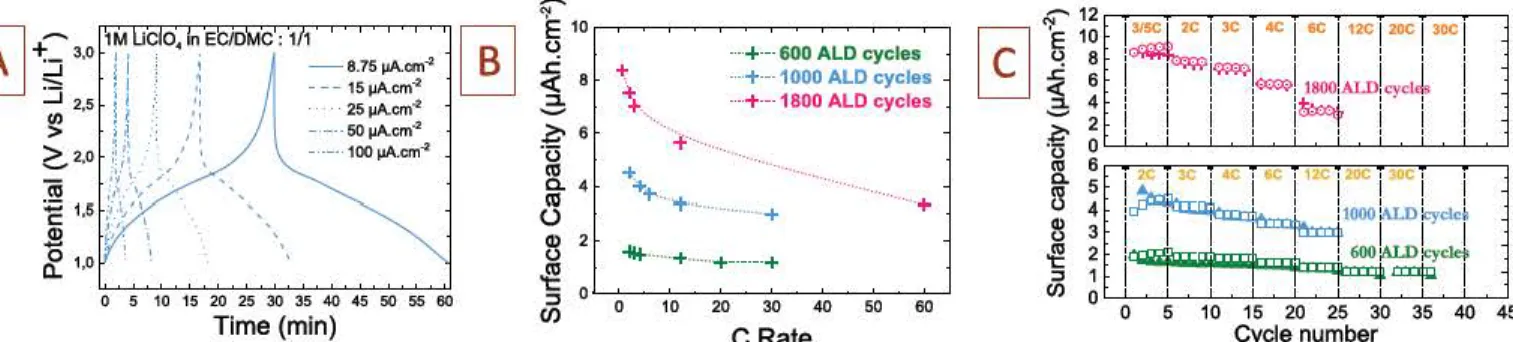
Fig. 6. Electrochemical analysis of the T-Nb:,O5 based on galvanostatic charge/discharge cycling. A. Galvanostatic plots at di&rent current densities
between
1 and 3V vs Li/Li•. B.Evolution of the surface capacity as a function of
the
C-rate for 3 different thickness (600, 1000 and 1800 ALD cycles respectively). C. Surface capacity of the T-Nb,O5 vs the number ofcycles.
higher than the one published by Baba et al.
[53]
. B.
Dunn et al. have
published in 2012 a study
[22]
dealing with pseudocapacitive behavior
of mesoporous Nb:!Os, depending on the type of polymorph. A 70 m
2.g
-1
T
Nb:!Os sample could achieve 500 F g
-
1at low s-weep rate, within 1.8
V. The areal capacity of such mesoporous
T
NbiO5 is then close to 0.35
µAhcm
-
2•
We have no information about the film thickness which
make not possible to calculate the normalized capacity. Such value is
lower than the area1 capacity reached by the T
Nb:!O5
synthesized by
AID.
Moreover,
despite interesting properties for large scale super
capacitors, the mesoporous T
Nb:!O5
developed by Dunn et al. is not
synthesized by ALD while this
deposition
technique is an attractive
solution for micro supercapacitors applications and more largely for
miniaturized energy storage devices due to the high adhesion proper
ties of the
AID
layers and the outstanding conformai shape of the
deposited thin films.
When increasing the potential scan rate, the mean slope decreases
which is assumed to be linked with ohmic and diffusion limitations.
Fig.
S
C shows the volumetric capacitance
(areal
capacitance divided
by the film thickness). At 10 mV s
-
1,the volumetric capacitance reaches
a maximum value then slightly decreases for longer deposition times
(or higher thickness). This shows that a film thickness around 50nm
allows for efficient electrochemical performance; also, there is only
small performance
decrease
for film thicknesses up to 80 nm. Same
trend is observed for higher scan rates; however, the smaller capacity
measured at 25 and lOOmvs
-
1supports the existence of kinetic
limitations (ohmic and/or diffusion).
These
results show that
ALD
process is efficient to prepare Nb:!Os electrodes exhibiting decent areal
and volumetric electrode capacity.
Galvanostatic charge
/
discharge experiments of the 50 nm thick T
Nb:!Os sample at various current
densities is shown in
Fig.
6
A
As
expected, the voltage profile is characteristic of Li
ion intercalation
process, with a means discharge potential of 1.5 V vs Li/Li
+
. The high
coulombic efficiency
(>
99% for the 50 nm thick sample) even at low
current density
(Fi
g. 6
A) highlights the absence of leakage current due
to parasitic redox reaction coming from impurities, which is also a key
advantage of the ALD technique.
The
change of the area1 electrode
capacity versus the C rate have been calculated from the galvanostatic
charge/discharge plots for ail the samples, and are plotted in
Fig.
6
B.
The
600
AID
cycles sample (30 nm thick film) exhibits a constant
surface capacity of about 1.5 µAh cm
-
2within the whole C rate range,
that is from
1
C (1 h charging time) to 30 C (2 min charging time). The
small thickness of this sample prevents the charge storage process to be
diffusion limited within the dense T
Nb:!Os layer. For thicker samples
(1000
ALD
cycles
=
50 nm thick and 1800 ALD cycles
=
90 nm thick),
the surface capacity is increased from 5
µAh
cm
-
2(50 nm thick) up to 8
µAh cm
-
2(90 nm thick sample) at
1 C rate. 40% of capacity loss is
measured from
1
C to 30 C for the 50 nm thick T
NbiO5
sample, and
43% capacity for 90 nm thick T
NbiO5
sample. The capacity decrease
for thicker films is assumed to originate from ohmic and
u
• diffusion
limitations in the bulk of the T
NbiO5
films, in agreement with the
preparation of dense, conducting additive free Nbiûs films.
However, a
40% capacity loss at 30 C rate still makes these thin films interesting
for micro devices applications. To confirm the
dense behavior of the
T
Nb:!Os, a comparison is
done
between the theoretical gravimetric
capacity of NbiO5
with the experimental one.
The theoretical gravi
metric capacity
Qg-this 205 mAh g
-
1taking into account two lithium
ions intercalated in the NbiO5
framework. We measure at the lower
s-weep rate (0.4 mvs
-
1)
a surface capacity 0..urf
-exp
close to 5 µAhcm
-
2with 50nm thick T
NbiO
5leading to
Q
0orm
~
=
lOOµAhcm
-2
µm
-
1and a volumetric capacity Qvo1~
-
lOOOmAhcm
-3
. The theoretical
bulk density of the NbiO5 is 4.6 g.cm
-3
. Consequently, if dense layer is
taking into account, the experimental bulk density approximates the
theoretical density:
Qg-eq,=
1000/4.6
=
217 mAh g
-
1.
This
value is close
to the theoretical value. Lower bulk density (i.e. use of porous thin film)
will lead to eccentric gravimetric capacity
(>
217mAhg
-
1)
taking into
account the measured surface capacity and the
film
thickness. Such
calculation clearly confirms the dense behavior of the Nb:!Os layers.
Fig.
6
C shows the change of the capacity with the cycle number for the
three samples with 30 nm, 50 nm and 90 nm thick T
NbiO5
films.
Samples exhibit a good cycling behavior up to 20 C and 30 C during the
first 35 cycles, thus validating the attractive performance of T NbiO5
thin films prepared from
ALD
technique for electrochemical energy
storage micro
device applications.
ALD being a powerful tool to achieve conformai deposition of thin
films
from several nanometers to
100
nm
on complex micro or
nanoarchitectured substrate exhibiting high specific area, future
works
will be devoted to the deposition of T
Nb:!Os on complex nanoarchi
tectured scaffold to improve the areal footprint electrode capacity.
4.
Conclusion
This paper reports about the synthesis and electrochemical analysis
of T
Nb:!Os electrode deposited by
AID
on Ahû
s
/Pt coated silicon
wafer.
Tens of nanometer thick dense a Nb:!Os thin films were grown
by ALD, transformed into T
NbiO5 polymorph by further annealing at
750 °C.
T
NbiO5
film thickness and the resulting electrode areal
capacity could be successfully controlled by playing with the number
of
AID
cycles.
The
electrochemical analysis reveals a lithium ion
intercalation redox mechanism in the
T
NbiO5
electrode.
An
electrode
area1 capacity of 8
µAh
cm
-
2could be achieved at 1 C rate, with only
40% capacity loss at 30 C (2 minutes discharging time). These results
shows that Atomic Layer Deposition technique can be used for the
fabrication of Nbi05
based on chip micro devices for Internet of
Things (IoT) and wireless sensor network applications.
Acknowledgments
This
research is financially supported by the ANR (Agence
Nationale pour la Recherche) within the
MINOTORFS
(Micro
[1] M. Létiche, E. Eustache, J. Freixas, A. Demortière, V. De Andrade, L. Morgenroth, P. Tilmant, F. Vaurette, D. Troadec, P. Roussel, T. Brousse, C. Lethien, Atomic layer deposition of functional layers for on chip 3D Li-ion all solid state microbattery, Adv. Energy Mater. 7 (2017).http://dx.doi.org/10.1002/aenm.201601402. [2] L. Baggetto, R.A.H. Niessen, F. Roozehoom, P.H.L. Notten, High energy density
all-solid-state batteries: a challenging concept towards 3D integration, Adv. Funct. Mater. 18 (2008) 1057 1066.http://dx.doi.org/10.1002/adfm.200701245. [3] C. Liu, E.I. Gillette, X. Chen, A.J. Pearse, A.C. Kozen, M.A. Schroeder,
K.E. Gregorczyk, S.B. Lee, G.W. Rubloff, An all-in-one nanopore battery array, Nat. Nanotechnol. 9 (2014) 1031 1039.http://dx.doi.org/10.1038/nnano.2014.247. [4] P. Huang, C. Lethien, S. Pinaud, K. Brousse, R. Laloo, V. Turq, M. Respaud,
A. Demortière, B. Daffos, P.L. Taberna, B. Chaudret, Y. Gogotsi, P. Simon, On-chip and freestanding elastic carbonfilms for micro-supercapacitors, Science 351 (2016).http://dx.doi.org/10.1126/science.aad3345.
[5] M. Létiche, K. Brousse, A. Demortière, P. Huang, B. Daffos, S. Pinaud, M. Respaud, B. Chaudret, P. Roussel, L. Buchaillot, P.L. Taberna, P. Simon, C. Lethien, Sputtered titanium carbide thickfilm for high areal energy on chip carbon-based micro-supercapacitors, Adv. Funct. Mater. 27 (2017).http://dx.doi.org/10.1002/ adfm.201606813.
[6] E. Eustache, C. Douard, A. Demortière, V. De Andrade, M. Brachet, J. Le Bideau, T. Brousse, C. Lethien, High areal energy 3D-Interdigitated micro-supercapacitors in aqueous and ionic liquid electrolytes, Adv. Mater. Technol. 1700126 (2017) 1700126.http://dx.doi.org/10.1002/admt.201700126.
[7] M.F. El-Kady, M. Ihns, M. Li, J.Y. Hwang, M.F. Mousavi, L. Chaney, A.T. Lech, R.B. Kaner, Engineering three-dimensional hybrid supercapacitors and microsu-percapacitors for high-performance integrated energy storage, Proc. Natl. Acad. Sci. USA 112 (2015) 4233 4238.http://dx.doi.org/10.1073/pnas.1420398112. [8] D. Pech, M. Brunet, H. Durou, P. Huang, V. Mochalin, Y. Gogotsi, P.-L. Taberna,
P. Simon, Ultrahigh-power micrometre-sized supercapacitors based on onion-like carbon, Nat. Nanotechnol. 5 (2010) 651 654. http://dx.doi.org/10.1038/nna-no.2010.162.
[9] Y.-Y. Peng, B. Akuzum, N. Kurra, M.-Q. Zhao, M. Alhabeb, B. Anasori, E.C. Kumbur, H.N. Alshareef, M.-D. Ger, Y. Gogotsi, All-MXene (2D titanium carbide) solid-state microsupercapacitors for on-chip energy storage, Energy Environ. Sci. 9 (2016) 2847 2854.http://dx.doi.org/10.1039/C6EE01717G. [10] A. Ferris, S. Garbarino, D. Guay, D. Pech, 3D RuO2microsupercapacitors with
remarkable areal energy, Adv. Mater. 27 (2015) 6625 6629.http://dx.doi.org/ 10.1002/adma.201503054.
[11] P. Huang, C. Lethien, S. Pinaud, K. Brousse, R. Laloo, V. Turq, M. Respaud, A. Demortiere, B. Daffos, P.L. Taberna, B. Chaudret, Y. Gogotsi, P. Simon, On-chip and freestanding elastic carbonfilms for micro-supercapacitors, Science 351 (2016) 691 695.http://dx.doi.org/10.1126/science.aad3345.
[12] M.F. El-Kady, R.B. Kaner, Scalable fabrication of high-power graphene micro-supercapacitors forflexible and on-chip energy storage, Nat. Commun. 4 (2013) 1475.http://dx.doi.org/10.1038/ncomms2446.
[13] E. Eustache, R. Frappier, R.L. Porto, S. Bouhtiyya, J.F. Pierson, T. Brousse, Asymmetric electrochemical capacitor microdevice designed with vanadium nitride and nickel oxide thinfilm electrodes, Electrochem. Commun. 28 (2013) 104 106. http://dx.doi.org/10.1016/j.elecom.2012.12.015.
[14] P. Simon, Y. Gogotsi, Materials for electrochemical capacitors, Nat. Mater. 7 (2008) 845 854.http://dx.doi.org/10.1038/nmat2297.
[15] T. Brousse, D. Belanger, J.W. Long, To be or not to be pseudocapacitive?, J. Electrochem. Soc. 162 (2015) A5185 A5189.http://dx.doi.org/10.1149/ 2.0201505jes.
[16] P. Gibot, M. Casas-Cabanas, L. Laffont, S. Levasseur, P. Carlach, S. Hamelet, J.-M. Tarascon, C. Masquelier, Room-temperature single-phase Li insertion/extrac-tion in nanoscale LixFePO4, Nat. Mater. 7 (2008) 741 747.http://dx.doi.org/
10.1038/nmat2245.
[17] M. Wagemaker, R. Van de Krol, A.P.M. Kentgens, A.A. Van Well, F.M. Mulder, Two phase morphology limits lithium diffusion in TiO2 (anatase): a 7Li MAS NMR study, J. Am. Chem. Soc. 123 (2001) 11454 11461.http://dx.doi.org/10.1021/ ja0161148.
[18] L. Wang, H. Li, M. Courty, X. Huang, E. Baudrin, Preparation and characterization of LiNi0.5Mn 1.5O4-δ thin films taking advantage of correlations with powder samples behavior, J. Power Sources 232 (2013) 165 172.http://dx.doi.org/ 10.1016/j.jpowsour.2012.10.099.
[19] R.A. Rani, A.S. Zoolfakar, A.P. O’Mullane, M.W. Austin, K. Kalantar-Zadeh, Thin films and nanostructures of niobium pentoxide: fundamental properties, synthesis methods and applications, J. Mater. Chem. A 2 (2014) 15683 15703.http:// dx.doi.org/10.1039/C4TA02561J.
[20] N. Özer, M.D. Rubin, C.M. Lampert, Optical and electrochemical characteristics of niobium oxidefilms prepared by sol-gel process and magnetron sputtering: a comparison, Sol. Energy Mater. Sol. Cells 40 (1996) 285 296.http://dx.doi.org/ 10.1016/0927-0248(95)00147-6.
[21] K. Brezesinski, J. Wang, J. Haetge, C. Reitz, S.O. Steinmueller, S.H. Tolbert, B.M. Smarsly, B. Dunn, Pseudocapacitive contributions to charge storage in highly ordered mesoporous group V transition metal oxides with iso-oriented layered nanocrystalline domains, J. Am. Chem. Soc. 132 (2010) 6982 6990. [22] J.W. Kim, V. Augustyn, B. Dunn, The effect of crystallinity on the rapid
pseudocapacitive response of Nb 2O 5, Adv. Energy Mater. 2 (2012) 141 148. http://dx.doi.org/10.1002/aenm.201100494.
[23] H. Sun, L. Mei, J. Liang, Z. Zhao, C. Lee, H. Fei, M. Ding, J. Lau, M. Li, C. Wang, X. Xu, G. Hao, B. Papandrea, I. Shakir, B. Dunn, Y. Huang, X. Duan, Three-dimensional holey-graphene/niobia composite architectures for ultrahigh-rate energy storage, Science 356 (2017) 599 604. http://dx.doi.org/10.1126/scien-ce.aam5852.
[24] J. Come, V. Augustyn, J.W. Kim, P. Rozier, P.-L. Taberna, P. Gogotsi, J.W. Long, B. Dunn, P. Simon, Electrochemical kinetics of nanostructured Nb2O5electrodes, J. Electrochem. Soc. 161 (2014) A718 A725.http://dx.doi.org/10.1149/ 2.040405jes.
[25] V. Augustyn, J. Come, M.A. Lowe, J.W. Kim, P.-L. Taberna, S.H. Tolbert, H.D. Abruña, P. Simon, B. Dunn, High-rate electrochemical energy storage through Li+ intercalation pseudocapacitance, Nat. Mater. 12 (2013) 518 522.http:// dx.doi.org/10.1038/nmat3601.
[26] C.-H. Lai, D. Ashby, M. Moz, Y. Gogotsi, L. Pilon, B. Dunn, Designing pseudoca-pacitance for Nb2O5/carbide-derived carbon electrodes and hybrid devices, Langmuir (2017) 9407 9415.http://dx.doi.org/10.1021/acs.langmuir.7b01110. [27] M. Létiche, M. Hallot, M. Huvé, T. Brousse, P. Roussel, C. Lethien, Tuning the
cation ordering with the deposition pressure in sputtered LiMn1.5Ni0.5O4thinfilm deposited on functional current collectors for Li-ion microbattery applications, Chem. Mater. 29 (2017) 6044 6057. http://dx.doi.org/10.1021/acs.chemma-ter.7b01921.
[28] Y. Kim, N.J. Dudney, M. Chi, S.K. Martha, J. Nanda, G.M. Veith, C. Liang, A perspective on coatings to stabilize high-voltage cathodes: LiMn1.5Ni0.5O4with sub-nanometer lipon cycled with LiPF6electrolyte, J. Electrochem. Soc. 160 (2013) A3113 A3125.http://dx.doi.org/10.1149/2.017305jes.
[29] S.M. George, Atomic layer deposition: an overview, Chem. Rev. 110 (2010) 111 131.http://dx.doi.org/10.1021/cr900056b.
[30] C. Detavernier, J. Dendooven, S. Pulinthanathu Sree, K.F. Ludwig, J.A. Martens, Tailoring nanoporous materials by atomic layer deposition, Chem. Soc. Rev. 40 (2011) 5242.http://dx.doi.org/10.1039/c1cs15091j.
[31] H.C.M. Knoops, M.E. Donders, M.C.M. van de Sanden, P.H.L. Notten, W.M.M. Kessels, Atomic layer deposition for nanostructured Li-ion batteries, J. Vac. Sci. Technol. A Vaccuum Surf. Film. 30 (2012) 010801.http://dx.doi.org/ 10.1116/1.3660699.
[32] B. Wang, Y. Zhao, M.N. Banis, Q. Sun, K.R. Adair, R. Li, T.K. Sham, X. Sun, Atomic layer deposition of lithium niobium oxides as potential solid-state electrolytes for lithium-ion batteries, ACS Appl. Mater. Interfaces 10 (2018) 1654 1661.http:// dx.doi.org/10.1021/acsami.7b13467.
[33] B. Wang, J. Liu, M. Norouzi Banis, Q. Sun, Y. Zhao, R. Li, T.K. Sham, X. Sun, Atomic layer deposited lithium silicates as solid-state electrolytes for all-solid-state batteries, ACS Appl. Mater. Interfaces 9 (2017) 31786 31793.http://dx.doi.org/ 10.1021/acsami.7b07113.
[34] S. Boukhalfa, K. Evanoff, G. Yushin, Atomic layer deposition of vanadium oxide on carbon nanotubes for high-power supercapacitor electrodes, Energy Environ. Sci. 5 (2012) 6872 6879.http://dx.doi.org/10.1039/c2ee21110f.
[35] R. Warren, F. Sammoura, F. Tounsi, M. Sanghadasa, L. Lin, Highly active ruthenium oxide coating via ALD and electrochemical activation in supercapacitor applications, J. Mater. Chem. A 3 (2015) 15568 15575.http://dx.doi.org/ 10.1039/C5TA03742E.
[36] R. Kodama, Y. Terada, I. Nakai, S. Komaba, N. Kumagai, Electrochemical and in situ XAFS-XRD investigation of Nb[sub 2]O[sub 5] for rechargeable lithium batteries, J. Electrochem. Soc. 153 (2006) A583.http://dx.doi.org/10.1149/ 1.2163788.
[37] A.A. Lubimtsev, P.R.C. Kent, B.G. Sumpter, P. Ganesh, Understanding the origin of high-rate intercalation pseudocapacitance in Nb2O5crystals, J. Mater. Chem. A 1 (2013) 14951.http://dx.doi.org/10.1039/c3ta13316h.
[38] D. Chen, J.H. Wang, T.F. Chou, B. Zhao, M.A. El-Sayed, M. Liu, Unraveling the nature of anomalously fast energy storage in T-Nb2O5, J. Am. Chem. Soc. 139 (2017) 7071 7081.http://dx.doi.org/10.1021/jacs.7b03141.
[39] J. Dendooven, C. Detavernier, Basics of atomic layer deposition : growth char-acteristics and conformalityAtomic Layer Deposition in Energy Conversion Applicationsfirst ed., Wiley-VCH Verlag GmbH & Co. KGaA., 2017, pp. 3 42.
fORte
densité d’énErgie sur Substrat rigide et flexible) project
(ANR 16 CE24 0012 01). The authors also want to thank the French
network on electrochemical energy storage (RS2E, ANR Labex
STORE EX)
for the financial support. The French RENATECH net
work is greatly acknowledged for the use of microfabrication facilities.
Chevreul Institute (FR 2638), Ministère de l’Enseignement Supérieur
et de la Recherche, Région Hauts de France and FEDER are acknowl
edged for supporting and funding XRD facilities.
Data availability
The raw/processed data required to reproduce these findings
cannot be shared at this time as the data also forms part of an ongoing
study.
Appendix A. Supplementary material
Supplementary data associated with this article can be found in the
online version at
doi:10.1016/j.ensm.2018.08.022
.
[40] K. Kukli, M. Ritala, M. Leskelä, R. Lappalainen, Niobium oxide thinfilms grown by atomic layer epitaxy, Chem. Vap. Depos. 04 (1998) 29 34.http://dx.doi.org/ 10.1002/(SICI)1521-3862(199801)04:01<29::AID-CVDE29>3.3.CO;2-I. [41] T. Blanquart, J. Niinistö, M. Heikkilä, T. Sajavaara, K. Kukli, E. Puukilainen, C. Xu,
W. Hunks, M. Ritala, M. Leskelä, M. Leskela, Evaluation and comparison of novel precursors for atomic layer deposition of Nb2O5Thin Films, Chem. Mater. 24 (2012) 975 980.http://dx.doi.org/10.1021/cm2026812.
[42] M. Grundner, J. Halbritter, XPS and AES studies on oxide growth and oxide coatings on niobium, J. Appl. Phys. 51 (1980) 397 405.http://dx.doi.org/ 10.1063/1.327386.
[43] K. Kim, M.S. Kim, P.R. Cha, S.H. Kang, J.H. Kim, Structural Modification of self-organized nanoporous niobium oxide via hydrogen treatment, Chem. Mater. 28 (2016) 1453 1461.http://dx.doi.org/10.1021/acs.chemmater.5b04845. [44] R. Romero, J.R. Ramos-Barrado, F. Martin, D. Leinen, Nb2O5thinfilms obtained
by chemical spray pyrolysis, Surf. Interface Anal. 36 (2004) 888 891.http:// dx.doi.org/10.1002/sia.1793.
[45] N. Özer, D.G. Chen, C.M. Lampert, Preparation and properties of spin-coated Nb2O5films by the sol-gel process for electrochromic applications, Thin Solid Films 277 (1996) 162 168.http://dx.doi.org/10.1016/0040-6090(95)08011 2. [46] S. Li, Q. Xu, E. Uchaker, X. Cao, G. Cao, Comparison of amorphous,
pseudohex-agonal and orthorhombic Nb2O5for high-rate lithium ion insertion,
CrystEngComm 18 (2016) 2532 2540.http://dx.doi.org/10.1039/C5CE02069G.
[47] P. Zaumseil, High-resolution characterization of the forbidden Si 200 and Si 222 reflections, J. Appl. Crystallogr. 48 (2015) 528 532.http://dx.doi.org/10.1107/ S1600576715004732.
[48] J.H. Klootwijk, K.B. Jinesh, F. Roozeboom, MIM in 3D: dream or reality?, Microelectron. Eng. 88 (2011) 1507 1513.http://dx.doi.org/10.1016/ j.mee.2011.03.137.
[49] S.B. Lee, G.W. Rubloff, ALD based metal-insulator-metal nanocapacitors for energy storage, ECS Trans. 25 (2009).http://dx.doi.org/10.1149/1.3205069(2049 2049).
[50] A.C. Kozen, A.J. Pearse, C.-F. Lin, M. Noked, G.W. Rubloff, Atomic layer deposition of the solid electrolyte LiPON, Chem. Mater. 27 (2015) 5324 5331.http:// dx.doi.org/10.1021/acs.chemmater.5b01654.
[51] M. Nisula, Y. Shindo, H. Koga, M. Karppinen, Atomic layer deposition of lithium phosphorus oxynitride, Chem. Mater. 27 (2015) 6987 6993.http://dx.doi.org/ 10.1021/acs.chemmater.5b02199.
[52] M. Létiche, E. Eustache, J. Freixas, A. Demortière, V. De Andrade, L. Morgenroth, P. Tilmant, F. Vaurette, D. Troadec, P. Roussel, T. Brousse, C. Lethien, Atomic layer deposition of functional layers for on chip 3D Li-Ion all solid state microbattery, Adv. Energy Mater. 7 (2017) 1 12.http://dx.doi.org/10.1002/aenm.201601402. [53] R. Ye, K. Ohta, M. Baba, Electrochemical properties of amorphous Nb2O5thinfilm
and its application to rechargeable thinfilm lithium ion batteries, ECS Trans. 73 (2016) 49 55.