HAL Id: hal-00491442
https://hal.archives-ouvertes.fr/hal-00491442
Submitted on 15 Jun 2010HAL is a multi-disciplinary open access
archive for the deposit and dissemination of sci-entific research documents, whether they are pub-lished or not. The documents may come from teaching and research institutions in France or abroad, or from public or private research centers.
L’archive ouverte pluridisciplinaire HAL, est destinée au dépôt et à la diffusion de documents scientifiques de niveau recherche, publiés ou non, émanant des établissements d’enseignement et de recherche français ou étrangers, des laboratoires publics ou privés.
From k
×p to atomic calculations applied to
semiconductor heterostructures
Laurent Pedesseau, Charles Cornet, François Doré, Jacky Even, Andrei
Schliwa, Dieter Bimberg
To cite this version:
Laurent Pedesseau, Charles Cornet, François Doré, Jacky Even, Andrei Schliwa, et al.. From k×p to atomic calculations applied to semiconductor heterostructures. Physics-based mathematical models of low-dimensional semiconductor nanostructures: analysis and computation, Nov 2007, Banff, Alberta, Canada. pp.012009, �10.1088/1742-6596/107/1/012009�. �hal-00491442�
From k·p to atomic calculations applied to semiconductor
heterostructures
L. Pedesseau1, C. Cornet1, F. Doré1, J. Even1, A. Schliwa2 and D. Bimberg2 1
FOTON-INSA Laboratory, UMR 6058 au CNRS, INSA de Rennes, 20 avenue des Buttes de Coëmes, CS 14315, 35043 RENNES Cedex, FRANCE.
2Institut für Festkörperphysik, Technische Universität Berlin, Hardenbergstrasse 36, 10623 Berlin, Germany
E-mail: laurent.pedesseau@insa-rennes.fr
Abstract. We present a brief overview of the main results obtained in our group for the simulation of electronic and optical properties of semiconductor heterostructures. A short introduction is given on InAs quantum dots, grown on InP, GaAs and GaP substrates. It is shown that 1-band k••••p calculations can be used in the reciprocal space, in order to get a simulation of perfectly ordered array of quantum dots. A semianalytical modeling is also presented, including an axial approximation of the 8*8 band k••••p calculations. Linear and non-linear contributions to piezoelectricity are discussed. A complete 8*8 band k••••p approach is then used to show the properties of InAs/InP quantum dots, with different substrate orientations. Finally, a study of the highly strained InAs/GaP interface is performed with a first principle modeling using ABINIT packages. Band lineups and evolution of gap energies are calculated, and compared to those found by Chuang et al. [1]
1. Introduction to InAs quantum dots
Recently there have been considerable research developments in the field of nano-structured semiconductor materials. In particular, quantum dots (QDs) may improve the properties of high performance optoelectronic devices as compared to that achieved with semiconductor quantum wells.[2] One of the biggest challenges for QD-optical-devices however is to reach specific wavelength with respect to targeted applications. In this respect, various materials associations are used. In our group, we devoted our researches to the study of InAs quantum dots. Using InAs/InP or InAs/GaAs QDs allows reaching respectively the 1.55 µm (0.8 eV) and 1.3 µm (0.95 eV) telecommunication wavelengths. In a more original approach, InAs/GaP QDs could be used to emit under the transparency region of the Silicon (>1.1 µm) for optical interconnection compatible with MOSFET technology.
In this regard, calculations of electronic and optical properties of quantum dots are a key step in the development of QDs-based applications. The simulation of QDs properties is most of the time performed using either atomistic models, such as the empirical pseudopotential theory,[3,4] or continuum models, such as the eight-band k••••p theory [5,6]. Our group was working on k••••p calculations over a decade evolving from 1-band to 8-band models. However, it appears necessary to use ab initio calculations in order to provide either input parameters for k••••p or to investigate new sort
of materials which include possible phase transition or non linear properties due to the high strained deformations. The following article presents in the section 2 a review of previous work e.g. section 2.1 and 2.3. Section 2.2 is an example of using ab initio parameters to start k••••p calculations with piezoelectric coefficients. Then, in the section 3, which is completely new, there are results on atomic calculations for highly strained InAs/GaP interfaces.
2. k·p approach
2.1. Extensions of the 1 band k••••p approach
The 1 band k••••p approach was used at the beginning of the study of InAs/InP QDs as a first approximation for the electronic properties. It suffers from several drawbacks like the lack of coupling between valence bands and conduction bands or approximate coupling to strains. The 1 band k••••p approach was however extended in our group to simulate the properties of vertically [7] or laterally [8] electronically coupled quantum dots. The case of lateral coupling was studied for organized arrays of quantum dots grown for ultralow-threshold laser devices [9] . The Fourier-transformed 1-band k••••p Schrödinger-type equation developed on a mixed basis of plane waves and Wannier states can thus be written:
k
c
'
k
E
k
)
r
V(
'
k
c
k
c
)
r
(
m
'
k
k k k k k k * r r r r r r r r r h r r r r r r r∑
∑
∑
+
=
∇
∇
−
1
2
2 , Withk
c
)
r
(
c
)
r
Ψ(
k k n n n r r r r r∑
∑
+
=
ϕ
This allows describing the wetting layer-assisted inter-QDs lateral (WLaiQD) coupling by studying the influence of wetting layer (WL) states on QDs states and vice-versa. The results performed on real samples QDs geometries show that WL and QDs have to be considered as a unique system, in strong coupling conditions. The increase of QDs density on the WL leads to enhanced splitting and minibands effects on QDs states. It induces a fragmentation of WL density of states interpreted as a 0D-like confinement of WL states. The charge redistribution efficiency between QDs is also increased in a laterally organized superlattice of coupled quantum dots [9].
2.2. Semi-analytical 8 band k••••p approach and axial approximation for (100) substrate
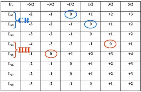
A complete semi-analytical model was then proposed for a more complete simulation of the electronic, mechanical and piezoelectric properties of narrow gap strained semiconductor quantum nanostructures [10, 11]. A transverse isotropic approximation for the strain and a new axial approximation for the strained 8x8 Hamiltonian is applied extensively to the case of InAs quantum dots (QD) grown on InP (100). By choosing the good quantum number Fz,[8] symmetry analysis shows that it does exist a non-vanishing splitting on the electron P states, due to the coupling with valence band. This splitting is found to be smaller in InAs/GaAs QD than in InAs/InP QD.
Figure 1: Block diagonalization of the Hamiltonian for each Fz value.
On figure 1, we reported values of Fz quantum number which is the total angular momentum according to Fz=Jz+Lz (Lz: the envelope function and Jz: the basis). The Conduction Band (CB) and the Valence Band (VB) ground states are associated, respectively, with Fz= ±1/2 and Fz= ±3/2. The degeneracies of CB and VB first excited states in the one-band representation (“CB 1P” and “HH 1P”) are lifted by the coupling to remote bands.
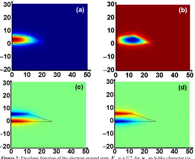
Figure 2 shows the most important components of the electron ground state
F
z=
+
1
2
for anInAs/InP truncated QD cone with 6nm for the truncation height. The weight of the u2 CB envelope function is equal to 93.3% with an S-like character (figure 2 (a)). We may notice that the weight of the
4
u HH P-like envelope function (figure 2 (b)) is not completely negligible and is equal to 1.2%. The other components with significant weights (above 1%) have S-like envelope functions. They correspond to the
u
3 LH (3.8%, figure 2 (c)) andu
8 SO (1.1%, figure 2 (d)) envelope function. We may notice that contrary to the two other ones, these envelope functions are located at the edges of the QD and have a nearly antisymmetric behavior with respect to a plane perpendicular to the z axis and located at the center of the QD. Indeed, it is straightforward to verify that in the case of a QD with a cylinder shape (D∞h symmetry instead of C∞v), these components are perfectly antisymmetric and the other ones symmetric.
Figure 2: Envelope function of the electron ground state
F
z=
+
1
2
for u2 an S-like character (a), for u4 an HH P-like character (b), for u3 LH P-like character(c), and for u8 SO P-like character (d).The anisotropic strain in and around of zinc-blende based semiconductor quantum dots (QD) can generate local piezoelectric charges. As a result, many degeneracies of the single particle energies, like the electron p-states, are lifted. The proper handling of the piezoelectric fields is an essential prerequisite for the electronic structure simulation. Analytic expressions for the P1 first order piezoelectric polarizations can thus be extracted, by using our semianalytical model.
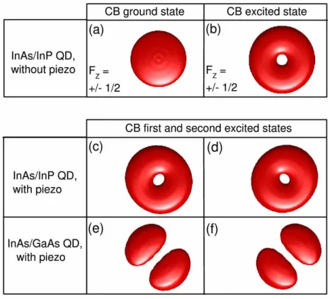
Figure 3:Comparison between the InAs/InP and the InAs/GaAs systems with the same QD geometry (height =2.9 nm). The isodensity surfaces containing 75% of the total density are shown for the (a) Fz=±1/2 CB ground state and the (b) Fz=±1/2 CB first excited state in the InAs/InP QD. Isodensity surfaces containing 75% of the total density for the eigenstates (c) and (d) obtained after applying the piezoelectric potential as a perturbation to the Fz=±1/2 CB and Fz=±3/2 CB first excited states in the InAs/InP QD. The same result is presented (e) and (f) for the InAs/GaAs QD.
We propose (figure 3) a comparison between the InAs/InP and the InAs/GaAs system with the same QD geometry (height=2.9nm). Due to the larger lattice mismatch in the InAs/GaAs case, a larger energy gap is found (0.90 eV for InAs/GaAs, and 0.78 eV for InAs/InP). Figure 3(a) and figure 3(b) represents respectively the isodensity surfaces containing 75% of the total density for the Fz
=
±
1
2
CB ground state and the Fz
=
±
1
2
CB first excited state (the difference with the CB Fz =±3 2 first excited state is very small). The piezoelectric potential obtained after solving the Poisson equation, is applied as a perturbation to the Fz =±1
2
CB and Fz =±3 2 CB first excited states. The amplitude of the piezoelectric potential is small for the InAs/InP QD. The resulting states (figures 3(c) and 3(d)) show only a small deviation from the cylindrical symmetry. The perturbation was then applied to the same states in the InAs/GaAs QD. The C2v symmetry clearly appears on figures 3(e) and 3(f).Recently it has been shown [3,4] that quadratic piezoelectric effect should be taken into account and may be greater than the linear one. Analytic expressions for the second P2 order piezoelectric polarizations can be calculated by using our semianalytical model.
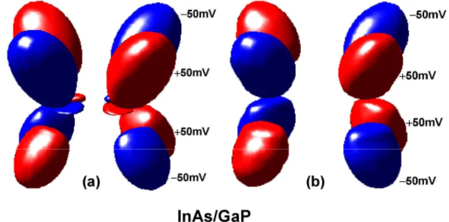
We should point out that the linear piezoelectric coefficients presented in Ref. 4 are larger than the classical ones we are using (InAs e14=−0.115 C.m−2, GaP e14=−0.15 C.m−2). We have used the same procedure to evaluate the second order piezoelectric coefficients for GaP using ab initio calculations: (InAs (Ref. 4), B114=−0.531 C.m−2, B124=−4.076 C.m−2, B156=−0.120 C.m−2; GaP, B114=−0.762 C.m−2, B124=−3.562 C.m−2, B156=−0.975 C.m−2). The corresponding piezoelectric potential can be calculated by solving the Poisson equation. Figure 4 presents a comparison of isosurfaces for ±50mV values of the piezoelectric potential in a conic InAs/GaP QD with a wetting layer for the case of the sum of linear and quadratic contributions (figure 4(a)) and for the case of the linear piezoelectric experimental constants (figure 4(b)). These figures are very close when we include the second order piezoelectric coefficient.
Figure 4: Isosurfaces for ±50 mV values of the piezoelectric potential in a conic InAs/GaP QD with a wetting layer are illustrated in the case of the sum of linear and quadratic contributions (a), and for the
linear piezoelectric experimental constants (b). 2.3. Complete 8*8 k••••p approach for misoriented substrates
A complete study of InAs/InP quantum dots by 8*8 band k••••p calculations has also been performed.[6] In this work, impact of substrate orientation and truncation height on optical properties have been examined carefully, with respect to experimental datas. As pointed out in ref. [6], a good agreement is found with experimental datas, and the importance of strain and piezoelectric field are considered as key parameters. Binding energies for trions (positive and negative), and also for biexciton have been calculated for InAs QDs on InP(100) substrate (figure 5 (a)) and on InP(311)B substrate (figure 5 (b)). As it’s well known for the case of small QDs, we obtain a positive binding energy for the whole. The case of large QDs is special so we observe a huge difference between both substrate orientations. Indeed, the piezoelectric potential is increased in the case of (311)B substrate, because in addition to the strain distribution around the QD, there is a contribution due to the non-standard substrate orientation.
Figure 5: Impact of the piezoelectric potential for InAs QDs on binding energies for trions (positive and negative), and for biexciton due to InP(100) substrate (a) and to InP(311)B substrate (b).
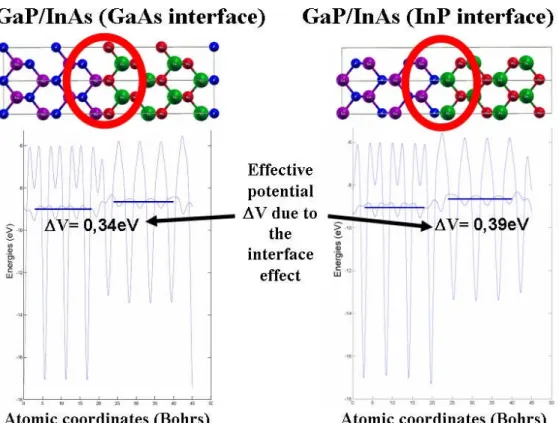
3. Atomic calculations by ab initio
The help of the ab initio calculation is needed in the case of highly strained deformations which induces non linear behavior. Our first aim is to compare the valence band line-up of InAs/GaP from existing calculations by Chuang [1] with Ab initio calculations. We perform our calculations using the density functional theory. We consider InAs/GaP small period superlattices with the local density approximation (LDA+GW) as pseudopotential. We do not include spin-orbit (SO) splitting in both calculations. We took into account 2 different interfaces e.g. GaAs and InP as one can see on figure 6. A correction via the GW approximation is made on each valence band. We had to calculate the average potentials in each crystal bulk, e.g. VInAs and VGaP and one can deduce easily the shift of about ∆V = 0.39 eV for InP interface. We found that the valence-band maximum in GaP is 9.9139 eV above VGaP and that in InAs is 10.8455 eV above VInAs. Finally, the discontinuity in the valence band of InAs/GaP is about Eν = 0.554 eV. Values of Qε are about 0.380 eV in the Chuang case and 0.378 eV
in the Ab initio case. Band lineups for strained InAs on GaP are thus determined. A good agreement is found between the classical linear and Ab initio calculations for the valence band. We then conclude that strain related non-linear evolutions of the gaps are associated to the conduction band behavior.
Figure 6: Effective potential ∆V for the InAs/InAs junction due to the interface effect for either GaAs or InP interface.
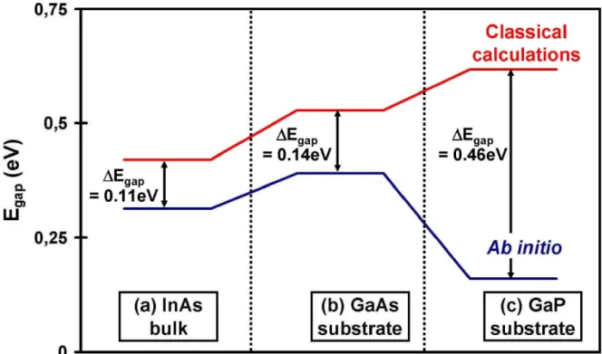
Evolution of the InAs gap energies for different biaxial deformations of the bulk crystal has been also studied. We define the biaxial deformation as
InAso InAs InAso
a
a
a
BD
====
−−−−
wherea
InAsois the lattice parameter of the InAs crystal without deformation anda
InAsis the lattice parameter including the deformation. There are two behaviors. The first behavior is an increase of the gap energy going through InP (BD=2.9%) substrate correspondence and finally reaching the GaAs (BD=6.6%) substrate correspondence. The second behavior is a non linear variation of the gap energy starting from GaAs to GaP (BD=9.9%) corresponding substrate. All along the linear case, as shown on figure 7(a-b), we underestimate the gap energy from about 0.11eV to 0.14eV in comparison with the classical calculation. In the non linear case, we calculate a decrease of the gap energy of about 0.46eV. This is due to the coupling between the conduction band corresponding to the lowest energy with other conduction bands located at higher energies (figure 7(c)).Figure 7: Gap energies for InAs crystal calculated for both Ab initio and classical calculations at 0 biaxial deformations (a), at BD corresponding to GaAs substrate (b), and at BD corresponding to GaP
substrate (c).
4. Conclusion
We have demonstrated that the k••••p 1 band approach can be used in the reciprocal space, in order to simulate the electronic properties of a full array of laterally organized superlattice of quantum dots. We have introduced a new axial approximation in the case of a conic InAs/InP(100) QD with a WL (8x8 k••••p Hamiltonian, linear and quadratic piezoelectric potential (ab initio parameters), excitonic effect …), and shown that it does exist a non-vanishing splitting of QDs energy levels, based on symmetry analysis. We applied the 8x8 k••••p band approach on InAs/InP QDs (311)B and (100) showing good agreement with the experimental datas. Finally, we obtained a good agreement between the valence band line-ups of InAs/GaP calculated either by a classical method or by Ab initio calculation then one can conclude that the non linear behavior of the gap energy is due to the conduction band.
We wish to acknowledge both European network of Excellence SANDIE and EPIXNET for theirs financial support to this research.
References
[1] S.-L. Chuang, “Physics of optoelectronic devices.” Wiley Series in pure and Applied Optics, Joseph W. Goodman, Series Editor, 1995.
[2] D. Bimberg, M. Grundmann, and N.N. Ledentsov, Quantum Dot Heterostructures (Chichester: Wiley, 1998).
[3] G. Bester and A. Zunger, Phys. Rev. B71, 045318-12 (2005).
[4] G. Bester, X. Wu, D. Vanderbilt and A. Zunger, Phys. Rev. Lett. 96, 187602-4 (2006). [5] O. Stier, M. Grundmann and D. Bimberg, Phys. Rev. B59, 5688-5701 (1999).
Simon, P. M. Koenraad, N. Bertru, D. Bimberg and S. Loualiche, Phys. Rev. B 74, 035312 (2006).
[7] P. Miska, J. Even, C. Paranthoen, O. Dehaese, A. Jibeli, M. Senes, X. Marie, Appl. Phys. Lett. 86, 111905 (2005).
[8] C. Cornet, C. Platz, P. Caroff, J. Even, C. Labbé, H. Folliot, A. Le Corre and S. Loualiche, Phys. Rev. B72, 035342 (2005).
[9] C. Cornet, C. Levallois, P. Caroff, L. Joulaud, E. Homeyer, C. Paranthoen, J. Even, C. Labbe, H. Folliot and S. Loualiche, Phys. Rev. B74, 245315 (2006).
[10] J. Even, F. Doré, C. Cornet and L. Pedesseau, Phys. Rev. B77, 085305 (2008).
[11] J. Even, F. Doré, C. Cornet, L. Pedesseau, A. Schliwa and D. Bimberg, Appl. Phys. Lett. 91, 122112 (2007).