UNIVERSITÉ DE MONTRÉAL
ORGANIC TRANSISTORS MAKING USE OF ROOM TEMPERATURE IONIC
LIQUIDS AS GATING MEDIUM
JONATHAN JAVIER SAYAGO HOYOS DÉPARTEMENT DE GÉNIE PHYSIQUE ÉCOLE POLYTECHNIQUE DE MONTRÉAL
THÈSE PRÉSENTÉE EN VUE DE L’OBTENTION DU DIPLÔME DE PHILOSOPHIÆ DOCTOR
(GÉNIE MÉTALLURGIQUE) AOÛT 2015
UNIVERSITÉ DE MONTRÉAL
ÉCOLE POLYTECHNIQUE DE MONTRÉAL
Cette thèse intitulée :
ORGANIC TRANSISTORS MAKING USE OF ROOM TEMPERATURE IONIC LIQUIDS AS GATING MEDIUM
présentée par : SAYAGO HOYOS Jonathan Javier en vue de l’obtention du diplôme de : Philosophiæ Doctor a été dûment acceptée par le jury d’examen constitué de :
M. MARTINU Ludvik, Ph. D., président
Mme SANTATO Clara, Doctorat, membre et directrice de recherche M. CICOIRA Fabio, Ph. D., membre et codirecteur de recherche Mme SOAVI Francesca, Ph. D., membre et codirectrice de recherche M. KÉNA-COHEN, Stéphane, Ph. D., membre
ACKNOWLEDGEMENTS
I would like to thank my research director, Clara Santato, for your faith, leadership, support and dedication in our time together at Polytechnique Montréal. Thanks to my co-directors, Francesca Soavi and Fabio Cicoira, for your kind advice and for working side by side with me at many different stages of this work. To my dear colleagues, Julia Wuensche, Sareh Bayatpour, Dilek Isik, Farzaneh Mahvash, Mitesh Patel, Prajwal Kumar, Irina Valitova, Zhihui Yi, Shiming Zhang, Xiang Meng, Eduardo Di Mauro, Francis Quenneville, Frédéric Venne, Umar Shafique, Olga Berezhetska, Ri Xu and Tian Lan, thanks for your companionship, generosity and friendship, I learned many things from you.
Thanks to our visiting students Gaurav Nanda, Jonathan Borduas, Ahcene Bayou and Étienne Bourbeau for your contribution as summer students to the present thesis.
Many thanks to Patricia Moraille, for your help in AFM, to Christophe Clément and Xavier Perraton for your assistance in microfabrication, to Josianne Lefebvre for your support in XPS measurements. Thanks to Jean-Paul Lévesque, Joël Bouchard, Yves Drolet, Yves Leblanc and Francis Boutet for your sensible and always well-timed help in the laboratories.
Thanks to Polytechnique Montréal for your academic and administrative services and to CONACYT for the scholarship grant to let me pursue a Ph.D. in Canada.
RÉSUMÉ
La capacité de transport ionique et électronique des couches minces organiques semiconductrices et conductrices est particulièrement intéressante dans le domaine de l’électronique imprimable et flexible.
L’incorporation d’un électrolyte en tant que milieu de grille dans les transistors organiques (Transistors EG), permet de moduler le courant en plusieurs ordres de grandeur à une tension relativement basse (<2 V) grâce à la capacitance exceptionnelle de l'interface du canal/électrolyte, déterminée par les faibles épaisseurs de la double couche électrique qui se forme à l’interface électrolyte/couche mince organique. Les liquides ioniques, soit des sels fondus à des températures inférieures à 100 °C, sont intéressants pour leur grande stabilité électrochimique (leur fenêtre de stabilité s’étend jusqu’à 5 V) et leur bonne conductivité ionique (1-15 mS cm-1). La principale motivation derrière le présent travail est de démontrer un fonctionnement à faible tension des transistors organiques en faisant usage des liquides ioniques, en tant que milieu de grille.
Tout d'abord, nous avons établi l'importance de la nature et morphologie de l’électrode de grille sur la performance des transistors électrochimiques. L’utilisation de carbone actif à haute aire de surface comme électrode de grille limite des processus électrochimiques indésirables à l’interface électrolyte/grille et rend inutile la présence d'une électrode de référence pour contrôler le potentiel du canal. Ceci a été démontré en utilisant des électrodes de grille en carbone actif, le polymère semiconducteur MEH-PPV comme matériel du canal et le liquide ionique [EMIM][TFSI] en tant que milieu de grille. L’utilisation de carbone actif avec une aire de surface non-limitative en termes de sa capacité à fournir la charge nécessaire pour moduler la conductivité du canal du transistor, a entraîné un voltage d’opération en dessous de 1 V et une mobilité des porteurs charge de (1,0 ± 0,5) × 10-2 cm2V-1s-1.
Un défi dans le domaine des transistors électrochimiques est d'améliorer le temps de réponse, qui est une conséquence du temps nécessaire pour la redistribution des ions dans le canal du transistor à l’application d’un biais électrique. Nous avons systématiquement étudié des transistors employant différents liquides ioniques appartenant à une même famille, c’est à dire basées sur un anion commun et des différents cations. Une influence limitée des différents cations
pour établir le dopage type-p du polymère conducteur fut démontré par les caractéristiques électriques des transistors. Il est intéressant de noter que le temps de réponse du transistor dépend d'au moins deux processus: la redistribution des ions de l'électrolyte vers le canal du transistor, qui affecte le courant grille-source (Igs), et la redistribution des charges dans le canal du transistor, qui affecte le courant drain-source (Ids) en fonction du temps. Les deux processus ont des vitesses différentes, ce dernier étant le plus lent. L'incorporation du carbonate de propylène dans l'électrolyte a été bénéfique pour réduire le temps de réponse du transistor.
Les fonctions de transistor et supercondensateur (TransCap), i.e. la fonction logique des transistors et le stockage d’énergie, au sein de la structure des transistors EG sont simultanément possibles. L'empilement polymère/électrolyte/carbone du transistor électrochimique comporte la configuration de cellule d'un supercondensateur hybride dont le carbone actif est chargé par un processus électrostatique et le canal du transistor est chargé par un processus électrochimique. Les supercondensateurs sont des systèmes à puissance spécifique élevée que pour leur capacité à stocker et fournir charge dans des délais courts, pourraient surpasser la performance des batteries dans les applications où une puissance élevée est nécessaire. Lorsque le TransCap est allumé (le canal du transistor est ouvert), le polymère et l’électrode de grille de carbone stockent une charge (Q) à une tension Vgs donnée, donc l'énergie stockée est égale à Q·Vgs. Lorsque le TransCap est éteint, le canal et la grille sont déchargés et l'énergie peut être livrée pour alimenter d'autres composants électroniques.
ABSTRACT
The ability to couple ionic and electronic transport in organic transistors, based on π conjugated organic materials for the transistor channel, can be particularly interesting to achieve low voltage transistor operation, i.e. below 1 V. The operation voltage in typical organic transistors based on conventional dielectrics (200 nm thick SiO2) is commonly higher than 10 V. Electrolyte-gated
(EG) transistors, i.e. employing an electrolyte as the gating medium, permit current modulations of several orders of magnitude at relatively low gate voltages thanks to the exceptionally high capacitance at the electrolyte/transistor channel interface, in turn due to the low thickness (ca. 3 nm) of the electrical double layers forming at the electrolyte/semiconductor interface. Electrolytes based on room temperature ionic liquids (RTILs) are promising in EG transistor applications for their high electrochemical stability and good ionic conductivity. The main motivation behind this work is to achieve low voltage operation in organic transistors by making use of RTILs as gating medium.
First we demonstrate the importance of the gate electrode material in the EG transistor performance. The use of high surface area carbon gate electrodes limits undesirable electrochemical processes and renders unnecessary the presence of a reference electrode to monitor the channel potential. This was demonstrated using activated carbon as gate electrode, the electronic conducting polymer MEH-PPV, poly[2-methoxy-5- (2′-ethylhexyloxy)-1,4-phenylene vinylene] channel material, and the ionic liquid [EMIM][TFSI] (1-ethyl-3-methylimidazolium bis(trifluoromethylsulfonyl)imide), as gating medium. Using high surface area gate electrodes resulted in sub-1 V operation and charge carrier mobilities of (1.0 ± 0.5) ×10
-2 cm2V-1s-1.
A challenge in the field of EG transistors is to decrease their response time, a consequence of the slow ion redistribution in the transistor channel upon application of electric biases. We systematically investigated EG transistors employing RTILs belonging to the same family, i.e. based on a common anion and different cations. The transistor characteristics showed a limited cation influence in establishing the p-type doping of the conducting polymer. Interestingly, we observed that the transistor response time depends on at least two processes: the redistribution of ions from the electrolyte into the transistor channel, affecting the gate-source current (Igs); and the redistribution of charges in the transistor channel, affecting the drain-source current (Ids), as a
function of time. The two processes have different rates, with the latter being the slowest. Incorporating propylene carbonate in the electrolyte proved to be an effective solution to increase the ionic conductivity, to lower the viscosity and, consequently, to reduce the transistor response time.
Finally, we were able to demonstrate a multifunctional device integrating the transistor logic function with that of energy storage in a supercapacitor: the TransCap. The polymer/electrolyte/carbon vertical stacking of the EG transistor features the cell configuration of a hybrid supercapacitor. Supercapacitors are high specific power systems that, for their ability to store/deliver charge within short times may outperform batteries in applications having high power demand. When the TransCap is ON (open transistor channel), the polymer and the carbon gate electrodes store charge (Q) at a given Vgs, hence the stored energy equals Q·Vgs. When the TransCap is switched OFF, the channel and the gate are discharged and the energy can be delivered back to power other electronic components.
EG transistors, making use of activated carbon as gate electrode and different RTILs as well as RTIL solvent mixtures as electrolyte gating medium, are interesting towards low voltage printable electronics. The high capacitance at the interface between the electrolyte and the transistor channel enables energy storage within the EG transistor architecture.
TABLE OF CONTENTS
ACKNOWLEDGEMENTS ... III RÉSUMÉ ... IV ABSTRACT ... VI TABLE OF CONTENTS ... VIII LIST OF TABLES ...XII LIST OF FIGURES ... XIII LIST OF SYMBOLS AND ABBREVIATIONS... XX LIST OF APPENDICES ... XXIV
CHAPTER 1 INTRODUCTION ... 1
1.1 Overview ... 1
1.2 Research problem ... 1
1.3 Motivation ... 2
1.4 Organization of the work ... 4
CHAPTER 2 ORGANIC SEMICONDUCTORS ... 6
2.1 Molecular structures ... 8
2.1.1 Small molecules ... 8
2.1.2 Polymers ... 10
2.1.3 Thin film morphology and its correlation with the film electrical and optical properties ... 12
2.2 Novel organic semiconductor processing techniques ... 19
2.3 Charge transport in organic semiconductors ... 20
2.4 The organic field-effect transistor ... 22
CHAPTER 3 ELECTROLYTE-GATED ORGANIC TRANSISTORS ... 29
3.1 Electrochemical capacitors ... 29
3.1.1 Electrochemical Impedance Spectroscopy ... 30
3.1.2 Cyclic voltammetry ... 31
3.2 Electrolyte-gated transistor device structure and working mechanism ... 32
3.3 Electrolyte materials as gating media ... 33
3.3.1 Electrolyte solutions ... 34
3.3.2 Room temperature ionic liquids ... 35
3.3.3 Ion gels, polyelectrolytes and polymer electrolytes ... 37
3.3.4 Ionic conduction and ionicity ... 37
3.4 Electrolyte-gated organic transistors: literature ... 38
CHAPTER 4 ARTICLE 1: LOW VOLTAGE ELECTROLYTE-GATED ORGANIC TRANSISTORS MAKING USE OF HIGH SURFACE AREA ACTIVATED CARBON GATE ELECTRODES ... 47
4.1 Authors ... 47
4.2 Abstract ... 47
4.3 Introduction ... 48
4.4 Results and discussion ... 49
4.5 Conclusions ... 55
4.6 Experimental ... 55
4.7 Acknowledgements ... 56
CHAPTER 5 ARTICLE 2: ELECTROLYTE-GATED POLYMER THIN FILM TRANSISTORS MAKING USE OF IONIC LIQUIDS AND IONIC LIQUID-SOLVENT MIXTURES ... 57
5.2 Abstract ... 57
5.3 Introduction ... 58
5.4 Results and discussion ... 59
5.5 Conclusions ... 66
5.6 Experimental ... 66
5.7 Acknowledgements ... 68
CHAPTER 6 ARTICLE 3: TRANSCAP: A MONOLITHICALLY INTEGRATED SUPERCAPACITOR AND ELECTROLYTE-GATED TRANSISTOR ... 69
6.1 Authors ... 69
6.2 Abstract ... 69
6.3 Introduction ... 69
6.4 Results and discussion ... 71
6.5 Conclusions ... 75
6.6 Acknowledgements ... 76
CHAPTER 7 COMPLEMENTARY RESULTS... 77
7.1 N-type electrolyte-gated PCBM organic transistors ... 77
7.1.1 Preliminary results of electrolyte-gated transistors making use of n-type PCBM channel material. ... 78
CHAPTER 8 GENERAL DISCUSSION ... 81
8.1 The effect of the physicochemical properties of the electrolyte in establishing the transistor characteristics ... 82
8.2 The importance of the nature and surface area of the gate electrode on the EG transistor drain-source current modulation and its energy storage properties ... 83
8.3 Properties of n-type PCBM EG transistors ... 85
8.5 Towards electrolyte-gated organic light-emitting transistors: advances and challenges ...
... 89
CHAPTER 9 CONCLUSION AND PERSPECTIVES ... 93
BIBLIOGRAPHY ... 95
LIST OF TABLES
Table 3.1: Physicochemical properties and anodic and cathodic limits of ionic liquids of interest in electrolyte-gated organic transistors.132 ... 36 Table 8.1: Comparison of EG organic transistors with organic and inorganic transistors making use of conventional dielectrics (not electrolyte). ... 82
LIST OF FIGURES
Figure 2.1. Molecular orbitals of benzene.42 Reprinted with permission. ... 6
Figure 2.2. Energy level diagram of (a) an isolated molecule, (b) organic solid with intermolecular interactions extending over a few molecules and (c) solid with intermolecular interactions extending over many molecules, compared to (b). The electron affinity, A, and ionization potential, I, are indicated for the solid (s) and gas (g) phase. P is the polarization energy, Eg the band gap, EF the Fermi level and VL is the vacuum level.43 Reprinted with
permission. ... 7 Figure 2.3. Molecular structure of common units in organic semiconductors.44 Reprinted with
permission. ... 8 Figure 2.4. Molecular structure of pentacene, rubrene and TIPS-pentacene.44 Reprinted with
permission. ... 9 Figure 2.5. Molecular structure of PCBM.49 Reprinted with permission. ... 10 Figure 2.6. (a) Molecular structure of P3HT and (b) lamellar thin film stacking.53 Reprinted with permission. ... 11 Figure 2.7. Molecular structure of MEH-PPV (left) and energy levels (right). The energetic levels were taken from Osikowicz et al.60 ... 12 Figure 2.8. Transmission electron microscopy (TEM) bright-field images of PCBM films
obtained from chlorobenzene solutions via spin-coating (a) and slow deposition from solvent-vapor saturated atmosphere from the same solvent (b). In the inset, selected-area electron diffraction patterns show the higher crystalline structure in (b) compared to (a).66 Reprinted with permission. ... 13 Figure 2.9. Reduced viscosity η/η* of MEH-PPV solutions in cyclohexanone (η* is 1.85 cp) vs concentration of the polymer solution.73 Reprinted with permission... 16
Figure 2.10. Parallel and perpendicular orientations of the MEH-PPV aromatic ring on the glass substrate surface.59 Reprinted with permission. ... 17
Figure 2.11. (a) Photoluminescence (PL) spectra of MEH-PPV film after subsequent 2h thermal treatments at different temperatures, increasing from room temperature to 140 °C. (b) Normalized PL spectra of poly(2,5-bis(cheolestranoxy)-1,4-phenylene vinylene) (BCHA-PPV) film processed at different temperatures. The molecular structure of BCHA-PPV is shown in the inset.72 Reprinted with permission. ... 18 Figure 2.12. Schematic representation of the electrospinning set-up.78 Reprinted with permission.
... 19 Figure 2.13. Field-effect mobility (μFE) as a function of the inverse temperature for single crystal
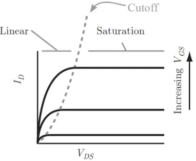
pentacene organic transistors (dots) and polycrystalline pentacene organic transistors (squares).82 Reprinted with permission. ... 21 Figure 2.14. Schematic representation of optical spectra of crystal and amorphous solid organic molecules.83 Reprinted with permission. ... 21 Figure 2.15. (a) Structure of a metal-insulator-semiconductor field-effect transistor and (b) ideal band diagram of the metal-insulator-semiconductor junction at equilibrium. The Fermi level (EF) and the intrinsic level (Ei) are located close to the midgap (Eg/2) for an intrinsic semiconductor. ... 23 Figure 2.16. Energy band diagram for a negatively polarized metal-insulator-semiconductor junction. ... 24 Figure 2.17. Schematic diagram of the transistor output characteristics. The transistor linear and saturation operation regimes and the cutoff line separating both regions are indicated.89
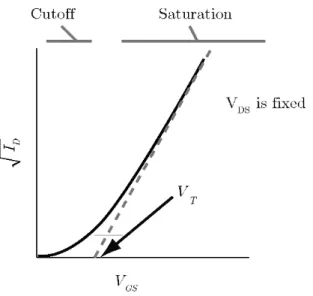
Reprinted with permission. ... 25 Figure 2.18. Illustration of the Ids1/2-Vgs transistor characteristics showing the extrapolation of
Ids1/2, to obtain Vt in the Vgs axis.89 Reprinted with permission. ... 27 Figure 3.1. Scheme of an electrolyte gated transistor and its equivalent electrochemical cell
electric circuit ... 31 Figure 3.2. Typical cyclic voltammetry shape for a single CV cycle ... 31 Figure 3.3. Schematic device structure of the electrolyte-gated organic transistor.38 Reprinted with permission. ... 32
Figure 3.4. Schematic of the working mechanism of a p-type electrolyte-gated transistor. a) electrostatic doping characterized by the formation of electrical double layers and b) electrochemical doping, where ion incorporation in the transistor channel takes place. ... 33 Figure 3.5. Schematic illustration of different types of electrolytes.112 Reprinted with permission.
... 34 Figure 3.6. Molecular structure of commonly used cations in ionic liquids.125 Reprinted with
permission. ... 35 Figure 3.7. Chemical structure of two triblock copolymers,
poly(styrene-b-methylmethacrylate-b-styrene) (PS-PMMA-PS) and poly(styrene-block-ethylene oxide-block-poly(styrene-b-methylmethacrylate-b-styrene) (PS-PEO-PS).99 Reprinted with permission. ... 39 Figure 3.8. Printed ion-gel gated polymer transistor. (a) Image of the aerosol-printed ion-gel polymer transistor array on a flexible polyimide substrate. The device channel length was 20 μm and channel width was 1400 μm. (b) Transfer characteristic (Vds= -1 V) and, on top, the device schematic cross-section diagram for devices employing P3HT channel material.143 Reprinted with permission. ... 40 Figure 3.9. Schematic illustration of the n-type electrolyte-gated single crystal transistors (top). A PDMS stamp moulded from a SU-8 photoresist relief was used as a substrate defining the drain-source interelectrode distance. L= 149 μm, W= 1 mm, and distance between the crystal and the recessed gate, d= 25 μm. Control devices were obtained by coating the substrate with a Ti/Au layer of 2/20 nm/nm, with a collimated flux of metal, and attaching a laminated single crystal on top of the channel. The final device structures were obtained by incorporating [PYR13][TFSI] ionic liquid as gating medium; the cross-section schematic of
the final device is shown. Transfer characteristics (bottom) and gate current, measured with
Vds =0.1, 0.2, 0.3, 0.4 and 0.5 V. The transfer characteristics of transistors employing air as gate dielectric are shown in the inset.147 Reprinted with permission. ... 41
Figure 3.10. All-organic, all-printed ion-gel gated P3HT transistor on flexible poly(ethylene naphthalate) substrates; device schematic (top) and transfer characteristics (bottom), Ids-Vgs, for Vds= -1V. The source and drain electrodes were made of PEDOT:PSS with an interelectrode distance, L= 50 μm, and width, W= 500 μm.142 Reprinted with permission. .. 43
Figure 3.11. Device structure of a microelectrochemical transistor including: source and drain electrodes, which, taken together with the open transistor channel, behave as the working electrode of the electrochemical cell, and a gate electrode, which behaves as the counter electrode in the electrochemical cell. The microelectrochemical transistor includes a reference electrode immersed in the electrolyte-gating medium.87 Reprinted with permission. ... 44 Figure 3.12. Transistor schematic formed at a fiber junction connected via an ionic liquid
electrolyte (top right). (a) transient plot, Ids vs time, measured by applying a gate voltage step from 0 to -1 V; in the inset, the transient plot at ms scale is shown to demonstrate electrostatic doping. (b) Transfer characteristics, Ids-Vgs, for Vds= -1 V, measured with a Vgs sweep at 0.33 V s-1.153 Reprinted with permission. ... 46 Figure 4.1. Device structure of the [EMIM][TFSI]-gated MEH-PPV transistors making use of an activated carbon gate electrode, in this work. The structure includes an activated carbon quasi reference electrode. A separator (Durapore® membrane filter, 9 mm × 4 mm × 125
µm) was soaked with [EMIM][TFSI] and placed on top of the MEH-PPV transistor channel (source-drain interelectrode distance, L, 10 µm, and electrode width, W, 4 mm). Two conducting carbon papers coated with activated carbon were set in contact with the separator and used as the gate (6 mm × 3 mm × 170 µm) and quasi reference (6 mm × 1 mm × 170 µm) electrodes. The molecular structures of the polymer MEH-PPV and the [EMIM][TFSI] ionic liquid are shown. ... 50 Figure 4.2. Electrochemical characteristics of [EMIM][TFSI]-gated MEH-PPV transistors. (a)
Cyclic voltammetry at 50 mV·s-1 obtained using the polymer film as the working electrode, the activated carbon gate electrode as the counter electrode and a second activated carbon electrode as the quasi reference electrode (black, solid line) or the carbon gate electrode itself as both the counter and the quasi reference electrode (red dotted line). In the latter case, the potential of the transistor channel corresponds to -Vgs (Vgs being the gate-source voltage). (b) Nyquist plot of the MEH-PPV working electrode at 0.8 V vs activated carbon, with the activated carbon gate electrode as the counter electrode and the small-sized activated carbon electrode as the quasi reference electrode. ... 52
Figure 4.3. Device characteristics of [EMIM][TFSI]-gated MEH-PPV transistors making use of activated carbon for the gate and the quasi reference electrode: (a) output characteristics (Ids vs Vds for Vgs = 0, -0.6, -0.65, -0.7, -0.75 and -0.8 V); (b) transfer characteristics in the saturation regime (Vds = -0.3 V), Ids (left axis, solid line) and Igs (gate-source current, right axis, dotted line) plotted vs Vgs, sweep rate 50 mV·s-1. Inset: transfer characteristics in the saturation regime (Vds=-0.3 V), for a sweep rate of 10 mV·s-1. ... 54 Figure 5.1. Device structure of the electrolyte-gated MEH-PPV transistors. A separator
(Durapore® membrane filter, 9 mm × 4 mm × 125 µm) was soaked in the electrolyte and placed on top of the transistor channel. Carbon paper coated with activated carbon was set in contact with the separator and used as the gate electrode (6 mm × 3 mm × 170 µm). The molecular structures of the polymer MEH-PPV and the ionic species [EMIM], [BMIM] , [PYR14] and [TFSI] are shown. ... 60
Figure 5.2. Atomic Force Microscopy height images (a-d, z-scale 10 nm), section profiles along the lines indicated in the height images (e-h), and phase images (i-l, z-scale 20°) of (a,e,i) MEH-PPV, (b,f,j) MEH-PPV:[EMIM][TFSI], (c,g,k) MEH-PPV:[BMIM][TFSI] and (d,h,l) MEH-PPV:[PYR14][TFSI] films. [MEH-PPV]:RTIL molar ratio of 1:0.5. ... 61
Figure 5.3. Device characteristics of electrolyte-gated MEH-PPV transistors making use of different ionic liquids. Left column: output characteristics (Ids vs Vds for Vgs = 0, 0.6, 0.65, -0.7, -0.75 and -0.8 V). Right column: transfer characteristics in the linear regime (Vds= -25 mV) for Vgs sweeping rate of 50 mV·s-1 (left axis, black solid line) and for Vgs sweeping rate of 10 mV·s-1 (left axis, black dotted line) together with I
gs (gate-source current, right axis blue line) vs Vgs for Vgs sweeping rate of 10 mV·s-1. In (a, b) the ionic liquid was [EMIM][TFSI], in (c, d) [BMIM][TFSI] and in (e, f) [PYR14][TFSI]... 62
Figure 5.4. Ids (left y axis) and Igs (right axis) vs time for a constant Vds of -300 mV applied to a [BMIM][TFSI]-gated MEH-PPV transistor before (solid lines) and after (dotted lines) addition of propylene carbonate. Vgs of -800 mV was applied at t=7.4 s for 5.5 s. ... 64 Figure 5.5. Device characteristics of the MEH-PPV transistor gated with [PYR14][TFSI] and a
drop of propylene carbonate (ca 15 μL of PC in 4.5 μL of [PYR14][TFSI]). (a) output
characteristics (Ids vs Vds, for Vgs = 0, -0.6, -0.65, -0.7, -0.75 and -0.8 V) and (b) transfer characteristics in the linear regime, Vds= -25 mV, for a Vgs sweeping rate of 50 mVs-1, left
axis black solid line, and sweeping rate of 10 mVs-1, left axis black dotted line, and I
gs (gate-source current, right axis blue line) plotted vs Vgs. ... 65 Figure 6.1. Device structure and working principle of the TransCap, whose proof-of-principle is proposed in this work. The drain (D) and source (S) electrodes and the p-doped MEH-PPV polymer channel are stacked with the electrolyte and the high surface area carbon gate. The polymer/electrolyte/carbon stacking features the cell configuration of a hybrid supercapacitor. ... 72 Figure 6.2. Transistor characteristics of the [N1113][TFSI]-gated MEH-PPV TransCap: (a) output
characteristics (Vgs = 0, -0.6, -0.65, -0.7, -0.75 and -0.8 V) and (b) transfer characteristics in the linear regime (Vds= -25 mV) for a Vgs sweeping rate of 10 mV s-1: Ids on the left axis, dashed line, and Igs on the right axis, solid line (please note that 0 V≤ Vgs ≤ -0.6 V do not significantly affect the transistor current). ... 73 Figure 6.3. Switch ON and OFF of the [N1113][TFSI]-gated MEH-PPV TransCap. Ids (left axis) and Igs (right axis) vs time for a switch ON at Vgs = -800 mV and switch OFF at Vgs=0 V. Vds = -300 mV. Data taken during a sequential type of acquisition (5.5 s TransCap ON followed by 5.5 s TransCap OFF): during the first 8 s, Vds = -300 mV and Vgs = 0 V... 74 Figure 6.4. Supercapacitor characteristics of the [N1113][TFSI]-gated MEH-PPV TransCap: (a)
voltage profile vs time when the device is galvanostatically charged/discharged at ±10 μA up to 0.8 V (data taken during the second cycle of a sequential type of acquisition: 6 s TransCap ON followed by 6 s TransCap OFF); (b) voltage (left axis) and current (right axis)
vs time upon galvanostatic charging at 10 μA up to 0.8 V, followed by 10 s at 0.8 V, 30 s
rest in open circuit conditions, and galvanostatic discharge at -10 μA. ... 75 Figure 7.1. (a) Schematic illustration and (b) optical top view of the [EMIM][TFSI]-gated C60
transistor. (c) Transfer characteristics including the gate current plotted in the right axis and (d) output characteristics of the [EMIM][TFSI]-gated C60 transistor.197 Reprinted with
permission. ... 78 Figure 8.1. Electrolyte-gated organic transistor: a) schematic device structure and b) image (top view) of a device where are shown the transistor channel, the square-shaped source and
drain electrodes, and the electrolyte, confined by a polydimethylsiloxane (PDMS) well. The substrate employed was glass or SiO2. ... 84
Figure 8.2. Process Flow to fabricate the MEH-PPV EG transistors. The substrate was a Si wafer (625 μm) with 200 nm dry thermal oxide (Silicon Quest International, Premium Grade). The electrolyte was [EMIM][TFSI], [BMIM][TFSI], [PYR14][TFSI] [N1113][TFSI] or
[BMIM][TFSI]-propylene carbonate (3:1 v:v) mixture, contained in a Durapore® membrane. ... 87 Figure 8.3. Process Flow to fabricate the PCBM EG transistors. The substrate was a Si wafer
(625 μm) with 200 nm dry thermal oxide (Silicon Quest International, Premium Grade). Drain and source electrodes were 5 nm/40 nm of Ti/Au. The electrolyte was [EMIM][TFSI], or [PYR14][TFSI], contained in a Durapore® membrane. ... 88
Figure 8.4. Organic light-emitting electrochemical transistor: a) device structure based on a PEDOT:PSS gate electrode, a KCF3SO3-PEO electrolyte, a MEH-PPV light-emitting
polymer semiconductor, and Au source and drain bottom electrodes; b) top view of the transistor channel, upon application of a cathode-anode voltage of 4 V a gate bias (VG) of 4
V (left) and -4 V (right); c) and d) proposed working principle for the light-emitting transistor upon application of positive (c) and negative d) gate bias. Adapted from.104 Reprinted with permission. ... 90 Figure 8.5. a) Device structure and b) p-type output characteristics of the organic electrochemical light-emitting field-effect transistor.233 reprinted with permission. ... 91
LIST OF SYMBOLS AND ABBREVIATIONS
A active surface area
AM-OLED active-matrix organic light-emitting diode [BMIM] 1-butyl-3-methylimidazolium BPhen 4,7-diphenyl-1,10-phenanthroline C capacitance CB conduction band CE counter electrode Ci capacitance density CV cyclic voltammetry e elementary charge E electric field Ea activation energy
EDL electrical double layer
EF Fermi level
Eg energy gap
EG electrolyte-gated
EG-OLET electrolyte-gated organic light-emitting transistor EIS electrochemical impedance spectroscopy
[EMIM] 1-ethyl-3-methylimidazolium
EOFF energy used to bring the transistor to the OFF state
EON energy used to bring the transistor to the ON state
EQE external quantum efficiency
F8BT poly(9,9′-dioctylfluorene-co-benzothiadiazole) Fc ferrocene [bis(n5-cyclopentandienyl)iron]
FOTS (tridecafluoro-1,1,2,2-tetra-hydrooctyl) trichlorosilane G-EML graded emissive layer
GOx glucose oxidase HMDS hexamethyldisilazane
HOMO highest occupied molecular orbital
I current
Ids source-drain current
IP ionization potential
IPA isopropyl alcohol
kB Boltzmann constant
L transistor channel length
LUMO lowest unoccupied molecular orbital
m mass of the electron
m* effective mass
MDMO-PPV poly(2-methoxy-5-(3’,7’-dimethyloctyloxy)-1,4-phenylenevinylene) MEH-PPV poly[2-methoxy-5-(2′-ethylhexyloxy)-1,4-phenylene vinylene] MISFET metal-insulator semiconductor field-effect transistor
[N1113] N-trimethyl-N-propylammonium
NMP N-methyl pyrrolidone OFET organic field-effect transistor OLED organic light-emitting diode OLET organic light-emitting transistor
p hole sheet charge carrier density
P power
P3HT poly(3-hexylthiophene) PBS phosphate buffered saline
PC propylene carbonate
PCBM [6,6]-phenyl-C61-butyric acid methyl ester
PDIF-CN2 N,N’’-bis(n-alkyl)-(1,7 and 1,6)-dicyanoperylene-3,4:9,10- bis(dicarboximide)
PDMS poly(dimethylsiloxane)
PEDOT:PSS poly(3,4-ethylenedioxythiophene):poly(styrenesulfonate) PEO poly(ethylene oxide)
PS-PEO-PS poly(styrene-block-ethylene oxide-block-styrene) PS-PMMA-PS poly(styrene-b-methylmethacrylate-b-styrene) PTFE polytetrafluoroethylene
PVA poly(vinyl alcohol)
[PYR14] 1-butyl-1-methylpyrrolidinium
Q sheet charge density
RT room temperature
RE reference electrode
RFID radio-frequency identification
rq root mean square roughness RTILs room temperature ionic liquids
rv sweep rate
T temperature
t time
TCTA 4,4′,4′′-tris(carbazol-9-yl) triphenylamine TIPS PENTACENE 6,13-bis(triisopropylsilylethynyl)pentacene
TPBi 2,2′,2′′-(1,3,5-benzinetriyl)-tris(1-phenyl-1-H-benzimidazole)
VB valence band
Vcell cell voltage
Vds source-drain voltage
Vfb flat-band potential
Vgs gate-source voltage
VL vacuum level
Vt threshold voltage
W transistor channel width
WE working electrode
XPS X-ray photoelectron spectroscopy
μ mobility
μFET field-effect transistor mobility
μo mobility prefactor
Φ metal workfunction
LIST OF APPENDICES
APPENDIX A – SUPPORTING INFORMATION FOR CHAPTER 4 ... 105 APPENDIX B – SUPPORTING INFORMATION FOR CHAPTER 5 ... 107 APPENDIX C – SUPPORTING INFORMATION FOR CHAPTER 6 ... 109 APPENDIX D – COMPLEMENTARY RESULTS ON PCBM ELECTROLYTE-GATED TRANSISTORS ... 112 APPENDIX E – COMPLEMENTARY RESULTS ON PCBM ELECTROLYTE-GATED TRANSISTORS ... 115 APPENDIX F – LIST OF PUBLICATIONS AT POLYTECHNIQUE MONTREAL NOT
INCLUDED IN THE THESIS ... 116 APPENDIX G – PARTICIPATION IN CONFERENCES AND MEETINGS ... 117
CHAPTER 1
INTRODUCTION
1.1 Overview
Organic electronic materials consist of π-conjugated molecules and polymers.2 Interest in organic electronic molecules is related to their tunable physico-chemical properties by chemical synthesis. For instance, light-emission can be achieved for virtually any color of the visible spectrum by tuning the molecular structure of organic electroluminescent materials.
In the 70’s, electrically conducting polymers exhibiting conductivities in the order of 30 S cm-1 were discovered.1 Later on, the first organic transistor was developed by in-situ polymerization of polyacetylene and polythiophene semiconducting thin films in the transistor channel.2
Organic electronic materials can be deposited over large areas from solution, e.g. using roll-to-roll processes.3–5 Since no covalent bond needs to be broken or re-formed during deposition, these materials offer high degree of mechanical flexibility and can be formed using a small energy input, i.e. with temperature < 200 °C, offering a route towards large area flexible organic electronics.
1.2 Research problem
Despite impressive improvements in material synthesis a number of challenges are open in the field of organic electronics. The charge carrier mobility typically seen in organic semiconductors remains low, i.e. mobilities in the range of 0.1-10 cm2V-1s-1 are considered state-of-the-art.6–8 Many organic semiconductors are not stable in ambient conditions partly because of their relatively low ionization potential (IP) of around 4.8 eV.3,9,10 Therefore they have to be processed in inert N2 atmosphere. Silanol groups present at SiO2 interfaces can quench n-type conductivity
in organic semiconductors that do not have sufficiently large electron affinities, i.e. <3.85 eV.11,12 From a device point of view, the operating voltage of organic transistors making use of a conventional 200 nm-thick SiO2 gate dielectric, is as high as 20-30 V.6 One strategy to lower the
In order to achieve low voltage operation, an interesting approach, for its compatibility with flexible electronics, is the use of electrolytes as gating medium. Coupling electrolytes and organic semiconductor channel materials can result in capacitances in the order of mF cm-2 at voltages below 2 V.18 Since the transistor current modulation is directly proportional to the capacitance, coupling electrolytes and organic semiconductor channel materials results in low voltage operation.
The principle of electrolyte-gating in a transistor channel has been known since almost sixty years, having been proposed by Shockley, Brattain and Bardeen.19,20
Wrighton and coworkers deeply investigated microelectrochemical transistors based on the electrolyte-gating principle.21–25 Ion-sensitive field-effect transistors,26–29 ion sensors30–32 and electrochemical transistors,21,25,33–37 have been demonstrated over the past 30 years.
More recently, Frisbie et al employed electrolyte-gated organic transistors to achieve low voltage electronics.38,39 Indeed, electrolyte-gating can be used to lower the operation voltage in organic transistors and as a tool to investigate the charge transport properties of organic semiconductor systems.
Another important advantage of electrolyte-gated transistors includes inherent low source and drain contact resistance.40 In electrolyte-gated organic thin film transistors the contact resistance has been shown to be orders of magnitude lower than in conventional organic transistors. This may be due to electrical double layer assisted charge injection, similar to what is observed in light-emitting electrochemical cells, where the active material comprises a blend of an ion-conducting electrolyte and a conjugated polymer.41
Despite the impressive capacitance values achievable in electrolyte-gated transistors, their response time is limited by ionic transport. For instance, while SiO2 can be polarized in the order
of 10-13 s, the polarization of electrolytes is limited by the ionic transport to set up the electrical double layers, usually in the order of a few seconds. These topics will be reviewed with further detail in Section 3.3.
1.3 Motivation
The main motivation of this work is to achieve large current modulation in organic electronic films using the configuration of electrolyte-gated (EG) transistors. Electrolyte-gating has been
revived with the appearance of a new class of electrolytes: room temperature ionic liquids (RTILs). RTILs exhibit high thermal stability, large electrochemical stability windows and good ionic conductivities. At present, most of the research efforts in the field of EG transistors focus on the transistor electrolytes and channel materials. Such efforts are presented in Chapter 3. Objectives
The specific objectives of this Ph. D. work are:
(1) To investigate the effect of the physicochemical properties of the electrolyte in establishing the transistor characteristics.
Strategy: The use of room-temperature ionic liquids belonging to the same family, i.e. sharing a common cation/anion, can elucidate the role of the doping ion and of the physicochemical properties of the electrolyte in the doping process.
Hypothesis: The molecular structure of the ions and the electrolyte physicochemical properties play an important role in the doping process. Electrolytes with high ionic conductivity and low viscosity should be able to dope faster the transistor channel. Bulky ionic structures should limit the permeation of ions into the transistor channel.
(2) To shed light on the importance of the nature and surface area of the gate electrode on the transistor drain-source current modulation and the operation voltage of the transistor.
Strategy: In situ electrochemical characterizations in the EG transistor channel, i.e. using the transistor channel as working electrode and the gate as counter electrode and reference electrode or using a third electrode as reference, can be an effective approach to investigate the electrolyte/gate and electrolyte/channel interfaces.
Hypothesis: The surface area and the nature of the gate electrode play an important role to avoid non-reversible electrochemical processes at the gate/electrolyte interface and to establish high current modulation at low voltages.
(3) To explore the possibility to combine energy storage function within the EG transistor structure.
Strategy: The EG transistor structures with high capacitance at the interface between the electrolyte and the transistor channel enables energy storage.
Hypothesis: The energy stored in EG organic transistors can be recovered to power other electronic components and is of interest for energy autonomous devices.
As a general strategy for the above objectives we make emphasis on polymer channel materials, for their simple processability and on room temperature ionic liquids as gating media, for their electrochemical stability and high ionic conductivity.
1.4 Organization of the work
In Chapter 2, we present an introduction to organic semiconductors and we introduce organic transistors and their figures of merit. In Chapter 3, we introduce the electrolyte-gated transistor structure and the electrolytes that can be employed as gating media. In the same chapter, we include a literature review about recent reports on electrolyte-gated organic transistors. Chapter 4 has been published as an article whose title is “Low voltage electrolyte-gated organic transistors making use of high surface area activated carbon gate electrodes” by J. Sayago, F. Soavi, Y. Sivalingam, F. Cicoira and C. Santato, in the Journal of Materials Chemistry C, 2014, 2, 5690. It discusses the importance of using gate electrodes with high surface area to supply the charge required to modulate the conductivity in the transistor channel with sub-1 V electrical biases. Chapter 5 was published as an article whose title is “Electrolyte-gated polymer thin film transistors making use of ionic liquids and ionic liquid-solvent mixtures”, by J. Sayago, X. Meng, F. Quenneville, S. Liang, É. Bourbeau, F. Soavi, F. Cicoira and C. Santato, in the Journal of Applied Physics, 2015, 117, 112809. It presents a systematic study of the effect of RTILs based on a common anion and RTIL-solvent mixtures on the transistor performance. Chapter 6 was published as an article whose title is “TransCap: a monolithically integrated supercapacitor and electrolyte-gated transistor” by J. Sayago, U. Shafique, F. Soavi, F. Cicoira and C. Santato, in the Journal of Materials Chemistry C, 2014, 2, 10273. It introduces the TransCap, a multifunctional Transistor-superCapacitor that combines the transistor logic function with the energy storage capability of supercapacitors. In Chapter 7, we include preliminary results of n-type EG PCBM transistors. Chapter 8 is a general discussion about the elements constituting the present work as a whole and Chapter 9 presents conclusions and recommendations for future work. An appendix
with supplementary information for Chapters 4-8 and a list of other publications and conferences is included.
CHAPTER 2
ORGANIC SEMICONDUCTORS
Organic materials, mainly composed of carbon atoms, are typically poor electronic conductors because electrons are confined locally in strong covalent sigma bonds. Nevertheless, organic compounds can become electronically conductive if they possess a carbon structure with regular alternation of single (σ) and double (σ and π) bonds, which is referred to as conjugation.
To illustrate the concept of conjugation, we refer to the molecular structure of benzene, Fig. 2.1. One 2s- and two 2p-carbon orbitals hybridize to form three sp2 hybrid orbitals on the same plane. The remaining pz-orbitals are perpendicular to that plane. The overlap of the hybridized orbitals
of one atom with the hybridized orbitals of neighboring atoms leads to the formation of σ bonds while the overlap of pz-orbitals generates π-bonds. If pz-orbitals overlap along a ring or an
extended carbon chain, the electrons are delocalized and can participate in charge carrier conduction. The overlap of two pz-orbitals results in one bonding π molecular orbital, with lower
energy than the atomic orbitals and one anti-bonding π* molecular orbital with higher energy than the atomic orbitals. The highest occupied molecular orbital (HOMO) is the occupied π-orbital with the highest energy and the lowest unoccupied molecular π-orbital (LUMO) is the unoccupied π*-orbital with the lowest energy. The energy gap between the HOMO and LUMO is the band gap (Eg), in this case, of benzene. The energy level of the HOMO and LUMO with respect to the vacuum level corresponds to the ionization potential and the electron affinity of the organic molecule.
In solid conjugated materials, both small molecules and polymers, charge carriers can move not only at the intramolecular level but also at the intermolecular level. The transition in the electronic structure from a single molecule (i.e. benzene) to a molecular solid is illustrated in Figs. 2.2a-c. When the intermolecular interactions are weak (van der Waals interactions, with typical energy < 0.2 eV), the electronic properties of the organic semiconductors are largely determined by the energy levels of the single molecules. As illustrated in Figs. 2.2a and 2.2b, the HOMO and LUMO levels of individual molecules merge into HOMO and LUMO bands for the organic solid.43 On the other hand, strong intermolecular interactions can result in long-range order with an important effect on the electronic properties of the solid. In this case, the HOMO and LUMO bands merge into a valence band and a conduction band with a much lower band gap, as illustrated in Fig. 2.2c.
Figure 2.2. Energy level diagram of (a) an isolated molecule, (b) organic solid with intermolecular interactions extending over a few molecules and (c) solid with intermolecular interactions extending over many molecules, compared to (b). The electron affinity, A, and ionization potential, I, are indicated for the solid (s) and gas (g) phase. P is the polarization energy, Eg the band gap, EF the Fermi level and VL is the vacuum level.43 Reprinted with
permission.
2.1 Molecular structures
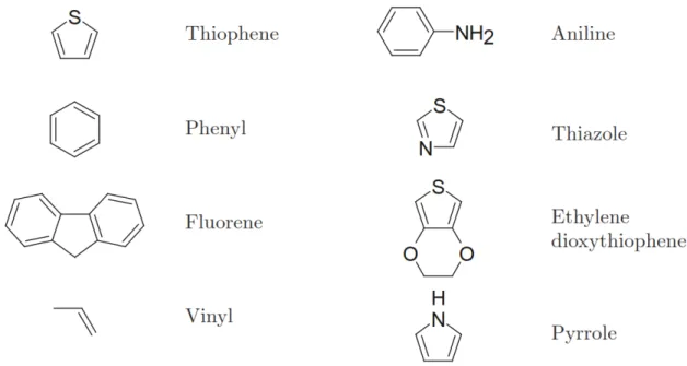
Organic semiconductors materials can be small molecules or polymers. Fig. 2.3 presents the molecular structure of common repeating units found in organic semiconductor materials.
Figure 2.3. Molecular structure of common units in organic semiconductors.44 Reprinted with
permission.
2.1.1 Small molecules
A category of organic semiconductors are π-stacked conjugated small molecules. Small molecules can form single crystals through π-π orbital overlap resulting in relatively high charge carrier mobility, i.e. 20 cm2V-1s-1.45
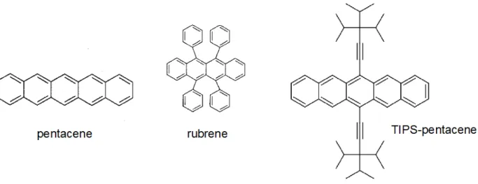
Charge transport in single crystal organic semiconductors is favoured by their highly regular, grain boundary-free structure. Particularly interesting small molecules in single crystal systems, for their good transport properties, are pentacene and rubrene, whose molecular structures are illustrated in Fig. 2.4.
Figure 2.4. Molecular structure of pentacene, rubrene and TIPS-pentacene.44 Reprinted with permission.
Pentacene is one of the most popular organic semiconductor materials used nowadays. It consists of five benzene rings linearly fused together, that are relatively easy to pack into ordered films. Pentacene thin films can reach charge carrier mobilities exceeding 1 cm2V-1s-1.3,46 It has been shown that polymorphic crystal growth can disrupt charge carrier transport due to the presence of grain boundaries.47 Because pentacene is not soluble, it can only be deposited by vacuum processes. However, synthetically attaching proper groups to the 6,13 positions of pentacene, such as in TIPS pentacene (Fig. 2.4), solubility in common organic solvents can be achieved.44 Rubrene is a fused ring semiconductor, illustrated in Fig. 2.4, which has attracted significant interest in its single crystal form. Rubrene holds the record for p-type charge transport in organic electronics with hole mobilities greater than 20 cm2V-1s-1.45
One example of n-type molecule is PCBM, illustrated in Fig. 2.5. Its lower LUMO level compared to C60 and C70 analogues allows easy electron injection. The electron mobility of PCBM thin films is ca 10-3 cm2V-1s-1.48,49
Figure 2.5. Molecular structure of PCBM.49 Reprinted with permission.
2.1.2 Polymers
Thin films of organic semiconducting polymers are particularly interesting for printable electronics since polymers can be designed to be soluble in different organic solvents and yield cost-effective deposition over large-areas, i.e. by roll-to-roll printing.38
One of the most popular conjugated polymers is poly(3-hexylthiophene), P3HT, a polythiopene derivative that employs alkyl side chains to improve its solubility without significantly disturbing its conjugated backbone.44 The molecular structure of conjugated polymers can be engineered to control the position of the solubilizing groups and yield head-tail head-tail (HT-HT) regioregular structures, as shown in Fig. 2.6a.50,51 Regioregular P3HT can self-organize into lamellar sheets, Fig. 2.6b, and feature charge carrier mobilities of up to 1 cm2V-1s-1.
The charge carrier mobility is not only affected by the film morphology but also by the molecular weight. Experimentally, it was observed that the mobility of spin-casted P3HT films could be increased from 10-6 cm2V-1s-1 to 10-2 cm2V-1s-1 by varying the molecular weight, from ca 3 kDa to 30 kDa.52
Figure 2.6. (a) Molecular structure of P3HT and (b) lamellar thin film stacking.53 Reprinted with permission.
At laboratory scale, P3HT thin films can be formed by spin-coating solutions of P3HT in high boiling point solvents, such as 1,2-dichlorobenzene, to promote slow drying and self-assembly on a flat SiO2 substrate.54 Often the substrate is pre-treated with hexamethyldisilazane (HMDS),
which creates a nonpolar hydroxyl-free surface that the hexyl groups of P3HT prefer. Thermal treatment under vacuum or inert N2 atmosphere is commonly employed to remove solvent traces
and to reverse possible p-doping that O2 could induce.55,56
A. Polyphenylene vinylene light-emitting polymers
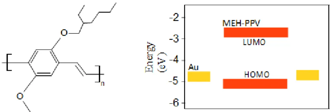
The demonstration of light-emitting diodes using electroluminescent polyphenylene vinylene (PPV) conjugated polymers in the 90’s paved the way towards polymer light-emitting devices.57 Since then, PPVs have been popular materials for their wide range of colour emission, from orange to green.58 A popular PPV, for its availability, processability and well known properties, is poly [2-methoxy-5-(2’-ethylhexyloxy)-1,4-phenylene vinylene] (MEH-PPV), illustrated in Fig. 2.7.59,60
Figure 2.7. Molecular structure of MEH-PPV (left) and energy levels (right). The energetic levels were taken from Osikowicz et al.60
2.1.3 Thin film morphology and its correlation with the film electrical
and optical properties
The molecular arrangement in organic semiconductor materials has an important effect on the film morphology and its electric and optical properties. Crystalline structures commonly feature high charge carrier mobilities but their processing commonly requires vacuum systems. Solution processing techniques, such as spin-coating, drop-casting, dip-coating and ink-jet printing, are generally simpler but the organic semiconductor has to be soluble.38 This is commonly achieved through molecular functionalization by adding alkyl chains or other bulky substituent groups. On the other hand, these groups can induce high steric hindrance limiting close intermolecular packing and resulting in poor charge carrier mobilities.61 The incorporation of semiconducting polymer films as active materials in electronic devices continues to be major research topic. The challenge relies on developing semiconducting polymers with high charge carrier mobility while keeping good processability and mechanical properties. Polymers usually cannot be grown into highly ordered single crystals. On the other hand, polymers may have the advantage of fast charge carrier transport along their conjugated backbone structure,62 except for some cases where
backbone tilting defects give rise to a distribution of shallow trap states in the gap and reduce the charge carrier mobility.63
A. Small molecule thin films
Physical vapor transport (PVT) of small molecules in a stream of high-purity noble gas (i.e. argon, helium) through horizontal reactors can produce highly pure single crystals.64,65 The reactor chamber is set with a narrow temperature gradient and the starting material is placed in the hottest region.
As an example of solution-processed small molecule thin films, we consider PCBM. Crystalline organization of PCBM from solution was reported by Yang et al. by using different solvents and different deposition techniques.66 PCBM films were obtained by spin-coating and, alternatively, from slow solvent evaporation in an atmosphere saturated with vapor of the corresponding solvent. The solvent-evaporation kinetics of film deposition played a major role in establishing the crystalline structure of the thin films. Spin-coated films (fast deposition) resulted in densely distributed PCBM nanocrystalline films with homogeneous morphology as illustrated in Fig 2.8a. By slow solvent evaporation conditions, large PCBM crystallites were observed, Fig. 2.8b.
Figure 2.8. Transmission electron microscopy (TEM) bright-field images of PCBM films obtained from chlorobenzene solutions via spin-coating (a) and slow deposition from solvent-vapor saturated atmosphere from the same solvent (b). In the inset, selected-area electron diffraction patterns show the higher crystalline structure in (b) compared to (a).66 Reprinted with permission.
Single crystal films of 2,7-dioctyl[1]benzothieno[3,2-b][1]benzothiophene (C8-BTBT) were obtained via ink-jet printing from solutions comprising a solvent and an anti-solvent (a liquid in which the semiconductor is insoluble).67 The solvent and anti-solvent were 1,2-dichlorobenzene (DCB) and N,N-dimethylformamide (DMF), both miscible with one another. This technique results in slower evaporation rates, about 10-50 times slower than in the case without the anti-solvent. Synchrotron single-crystal X-ray diffraction was used to determine the crystallinity of the thin films. Film thicknesses about 30-200 nm were obtained with mobilities exceeding 16 cm2V-1s-1.
Solvent vapor annealing of spin-coated thin films of C8-BTBT, an air stable and high-mobility semiconductor, has been reported.68 C8-BTBT was first spin-coated on SiO2 substrates
pre-treated with PMMA and then annealed for 10 h in chloroform vapors, resulting in single-crystal structures. Band-like charge transport (see Section 2.3.2) was observed with hole mobilities up to 9 cm2V-1s-1.
Single crystals of 3,11-didecyldinaphtho[2,3-d:2’,3’-d’]benzo[1,2-b:4,5-b’]dithiophene [C10-DNBDT] were obtained by a modified edge-casting solution crystallization technique.69 The substrate, a 100-nm thick thermally oxidized SiO2 layer, was treated with a phenyl-substituted
silane-based self-assembled monolayer [trimethoxy(2-phenylethyl)silane, β-PTS] to increase the wettability of the solution on the substrate. A mobile solid blade edge with a replenishing mechanism was used to supply solution at the same rate as the solvent evaporates resulting in inch sized single crystals, as confirmed by X-ray diffraction measurements. The p-type field-effect transistor mobility was 9.5 cm2V-1s-1 in the saturation regime and 8.2 cm2V-1s-1 in the
linear regime.
B. Polymer films
The processing conditions affecting the film morphology may affect different functional film properties, in different manners. Important factors, that will be discussed in this section, include the substrate chemistry and substrate morphology, the solution properties (concentration, solvent type and viscosity), the deposition conditions (atmosphere and temperature) and post-thermal treatments commonly employed to increase molecular ordering and to remove solvent traces.70,71 Hence it is paramount to understand the interplay between processing conditions, morphology
and structure of the films for the realization of high performance organic electronic materials and devices.
The correlations between morphology and electrical and optical properties in polymer thin films deposited from solution have been reviewed, among others, by Yang et al.59,72
Effect of the solution properties on the polymer film morphology
Molecules in solutions tend to aggregate when the concentration attains a critical value. The origin of molecular aggregation is the presence of intermolecular forces between polymer chains and polymer chain-solvent molecules.59 The solution viscosity is proportional to the intermolecular forces between the solvent molecules, i.e. higher solution viscosity suggests higher solvent intermolecular forces.
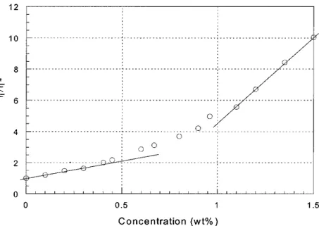
Shi et al proposed a method for characterizing the solution viscosity as a function of the solution concentration. The method is based on the reduced viscosity η/ η*, where η is the viscosity of the polymer solution and η* is that of the solvent, at room temperature.73 A plot (Fig. 2.9) of the
reduced viscosity of the polymer solution vs the polymer concentration (wt %) reveals three regimes. A linear regime at low concentration (i.e. <0.4%) where the polymer chains are not aggregated. A second linear region at high concentration (i.e. >0.9%) resulting in heavily aggregated polymer chains. The middle curved region can be defined as the region of concentration for loose aggregation.
Figure 2.9. Reduced viscosity η/η* of MEH-PPV solutions in cyclohexanone (η* is 1.85 cp) vs concentration of the polymer solution.73 Reprinted with permission.
The dependence of aggregation on solution concentration was observable by UV-Visible absorption spectroscopy.73 High concentrations, 1 wt%, resulted in an absorption λmax located at
496 nm while small concentrations, 0.3 wt%, resulted in a red shift of λmax, at 510 nm, thus
suggesting larger conjugation lengths for the latter. The optical properties at small and high concentrations were weakly influenced by the rotation spin speed applied during deposition suggesting that in these regimes the polymer stacking was stable enough to prevent changes by the centrifugal force or during the solvent evaporation. As the concentration approached the region for loose aggregation (0.7 wt%) the λmax in the electroluminescence spectra red-shifted
from ca 499 nm to ca 509 nm with increasing spin speed from 2000 rpm to 8000 rpm. During spin-coating, the centrifugal force and the radial flow of the solvent tend to stretch the polymer chains radially against the cohesive forces of the solution. If the centrifugal force is larger than the cohesive force of the solution, more extended (less coiled) conformations of the polymer molecules can be expected, resulting in more extended conjugation. Lower spin rates result in a more dense and thick films.
The solvent properties also play an important role on the conformation of MEH-PPV films.73
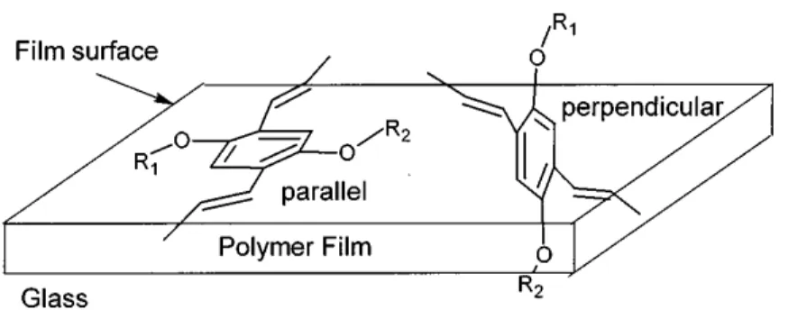
Thin films deposited using non-aromatic solvents result in more hydrophilic film surfaces suggesting that the film is more polar compared to those deposited using aromatic solvents. Since the polar components of MEH-PPV come from its C-O bonds, the surface polarity depends on how many C-O bonds are available on the surface to interact with water molecules during the hydrophilicity test. The more parallel conformation of the aromatic ring to the film surface (Fig. 2.10) exposes both oxygen atoms resulting in a more polar surface compared to a perpendicular conformation that only exposes one of the two oxygen atoms on the surface. Therefore, films deposited with non-aromatic solvents probably have a more parallel conformation than films deposited with aromatic solvents.
The solvent evaporation rate during deposition can also affect the conformation of MEH-PPV films.59 Lower solvent evaporation rates give to the polymer chains more time to relax into their more thermodynamically favorable conformation, i.e. parallel to the surface for glass substrates, as illustrated in Fig. 2.10.59 Treating the substrate surface with a self-assembled monolayer, i.e. octadecylmercaptan (ODM), can lower the substrate surface energy facilitating the parallel conformation of the film over the substrate.74
Figure 2.10. Parallel and perpendicular orientations of the MEH-PPV aromatic ring on the glass substrate surface.59 Reprinted with permission.
B. Effects of the post-deposition thermal treatment on the emission spectra
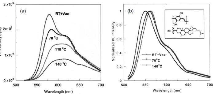
Post-deposition thermal treatments of polymer thin films can dramatically change their morphology. At temperatures above the glass transition temperature Tg, i.e. the temperature where the polymer evolves from a hard, glassy material to a soft, rubbery material, i.e. 75 °C for MEH-PPV, polymer chains tend to relax to more thermodynamically stable conformations.72 As illustrated in Fig. 2.11a, higher annealing temperatures result in red-shift MEH-PPV emission spectra and lower photoluminescence (PL) intensity. The lower PL intensity at higher temperatures has been attributed to interchain interactions leading to quenching of emission. A weaker effect of the temperature was observed on the normalized PL characteristics of BCHA-PPV, Fig 2.11b. Compared to MEH-BCHA-PPV, BCHA-PPV is a poly(p-phenylene vinylene) with larger side groups. The bulky side groups inhibit interchain interactions making BCHA-PPV less sensitive to the thermal treatment.
Figure 2.11. (a) Photoluminescence (PL) spectra of MEH-PPV film after subsequent 2h thermal treatments at different temperatures, increasing from room temperature to 140 °C. (b) Normalized PL spectra of poly(2,5-bis(cheolestranoxy)-1,4-phenylene vinylene) (BCHA-PPV) film processed at different temperatures. The molecular structure of BCHA-PPV is shown in the inset.72 Reprinted with permission.
2.2 Novel organic semiconductor processing techniques
Deposition methods to attain specific morphologies non-achievable by traditional deposition techniques such as spin-coating or drop-casting, are under development.
Molecular alignment using zone-casting, a deposition technique from solution, was reported by Tsao et al.75 A solution is spread out by means of a nozzle. The support moves after a critical concentration is attained (after solvent evaporation) this way forming an aligned thin film.
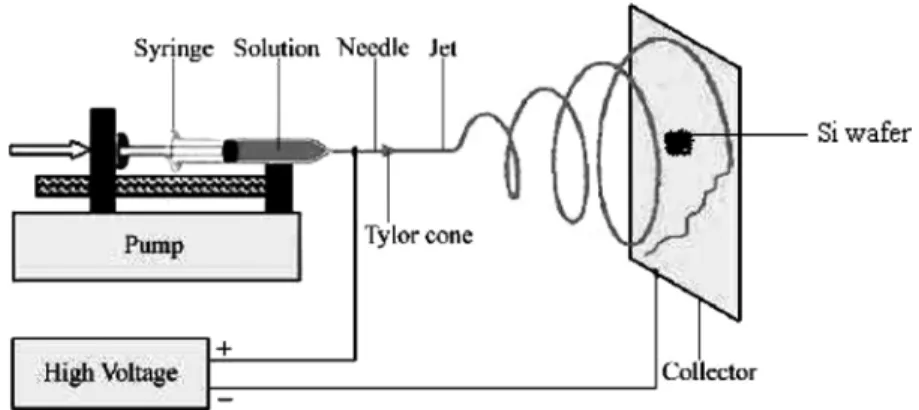
Polymer nanofiber films can be created by the electrospinning process.76The main advantage of electrospinned layers is the possibility to create fibers with high surface-to-volume ratio. The process of electrospinning is illustrated in Fig. 2.12. It uses an electrostatic force to spin polymer fibers from a nozzle of a syringe containing a polymer solution onto a substrate. The needle is maintained at a certain voltage with respect to the target substrate, by a power supply. When the electrostatic force overcomes the surface tension of the polymer solution, the liquid spills out of the spinneret and forms fine filaments, which are collected on the substrate. This method allows to produce fibers with diameters ranging from 2 nm to several microns and gives a unique opportunity to control the size of the voids between fibers.77
Figure 2.12. Schematic representation of the electrospinning set-up.78 Reprinted with permission.
Controlled alignment and patterning of single p- and n- type polymer nanowires was demonstrated using an electrospinning variant, high-speed electrohydrodynamic organic nanowire printer. Single nozzle electrospinning of P3HT/PEO solutions resulted in field-effect mobilities of 3.8 cm2V-1s-1.79
2.3 Charge transport in organic semiconductors
One of the figures of merit to quantify charge transport is the charge carrier mobility. The charge carrier mobility (μ) is the ratio between the average charge carrier speed (v) and the electric field (E) in the material.
E
v
=
µ
. Eq. (1)Different mechanisms have been proposed to describe charge transport in organic semiconductors. They will be briefly reviewed in what follows.
In semiconductors such as Si or Ge, characterized by a regular lattice arrangement of atoms, coulombic interactions between electrons and holes are weak (with energy <100 meV) due to strong dielectric screening, and electrons and holes are nearly free (bounded in a crystalline structure) to move at room temperature.80
Charge carrier transport in such materials has been modelled employing the concept of “bands” described at the beginning of the present chapter. The band transport model is valid only when the charge carrier mean free path (distance between scattering events) is larger than the crystalline lattice constant.80
In the band transport model, the mobility depends on the temperature (T) as: 81
n
T
−∝
µ
with n ~ 1-2 Eq. (2)For example, Fig. 2.13 shows a plot of the mobility as a function of the temperature for polycrystalline pentacene- and single crystal pentacene-based transistors (see also section 2.4.1.). The mobility of single crystal pentacene (dots) can be fitted well to Eq. (2), thus indicating band transport. The mobility of polycrystalline pentacene (squares) first increases with temperature to a maximum value of ca 0.4 cm2Vs-1 at ca 240 K and then sharply decreases as a function of temperature as opposed to single crystal pentacene organic transistors.
Figure 2.13. Field-effect mobility (
μ
FE) as a function of the inverse temperature for single crystalpentacene organic transistors (dots) and polycrystalline pentacene organic transistors (squares).82 Reprinted with permission.
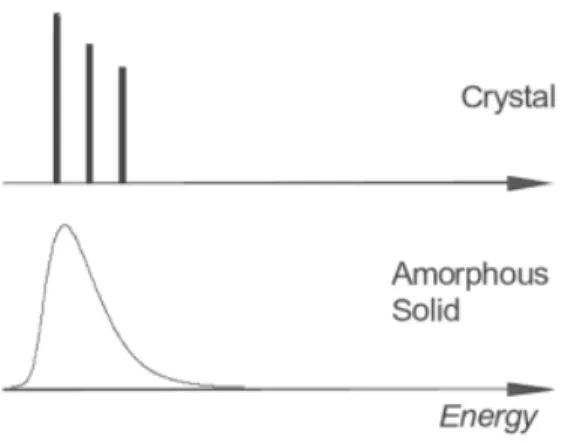
The band transport behaviour is rarely observed in organic semiconductors, except for some organic single crystals. Organic semiconductors are commonly characterized by a Gaussian distribution of the HOMO and LUMO levels.80 Amorphous and polycrystalline organic solids usually show considerable spectral broadening as schematically illustrated in Fig. 2.14.
Figure 2.14. Schematic representation of optical spectra of crystal and amorphous solid organic molecules.83 Reprinted with permission.
Charge carriers in amorphous and polycrystalline organic semiconductors usually hop between different sites and the mobility dependence on the temperature is described by an Arrhenius-type relation84 − = T E μ μ a O B k exp Eq. (6)
with a prefactor μo and an activation energy Ea (kB is the Boltzmann constant).
One notable limitation of the hopping transport model is to consider Ea constant while experimentally it has been observed that Ea decreases with the increase of the applied gate voltage (Vgs).85,86 Because the charge carrier density increases with the increase of Vgs, affecting other material properties as well, reviewed in Section 2.4, it is reasonable to propose a correlation between the activation energy and the charge carrier density.87
The multiple trap and release transport model, originally conceived to model the mobility in hydrogenated amorphous silicon thin films, predicts a mobility dependence upon temperature and gate voltage, as observed experimentally in organic transistors.
Horowitz et al developed a semi-empirical mobility expression for organic transistors as a function of the gate-source voltage (Vgs).85
T T T to gs i to C o C
eN
V
C
N
N
μ
μ
−
=
Eq (7)where NC is the effective density of states in the transport energy level, Nto is the surface density of traps at the semiconductor-insulator interface of the transistor channel, Ci is the specific capacitance of the insulator, e is the elementary charge and TC is a characteristic temperature related to the width of the exponential trap distribution.
2.4 The organic field-effect transistor
The organic transistor emulates, with organic semiconducting materials, the structure of the metal-insulator-semiconductor field-effect transistor (MISFET) that is a key component in most electronic devices, for example, microprocessors, memory devices, active-matrix displays.
Modern computing power is based on single-crystalline silicon semiconductors that can reach carrier mobilities in the order of 102-103 cm2V-1s-1. Although organic transistors, with an organic
semiconductor channel, cannot compete with these mobilities, they may be employed in alternative applications such as sensors or radio-frequency identification (RFID) tags or in applications where mechanical compliance is required.3,53
The typical structure of an organic transistor and the energy levels for the metal-insulator-semiconductor junction are illustrated in Fig. 2.15a and Fig. 2.15b.88 The transistor structure consists of an organic semiconductor included between source and drain electrodes and stacked with a dielectric and gate electrode. The region delimited by the source (S) and the drain (D) electrodes defines the transistor channel, with a geometry characterized by the interelectrode distance (channel length, L), the electrode width (channel width, W) and the channel thickness (t). Upon application of an appropriate gate-source bias (Vgs), electronic charge carriers can be induced in the transistor channel and move under the action of a source–drain bias (Vds). The current flowing between S and D (Ids) is modulated by Vgs. The source electrode is usually the common ground.5
Figure 2.15. (a) Structure of a metal-insulator-semiconductor field-effect transistor and (b) ideal band diagram of the metal-insulator-semiconductor junction at equilibrium. The Fermi level (EF) and the intrinsic level (Ei) are located close to the midgap (Eg/2) for an intrinsic semiconductor.