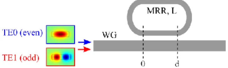
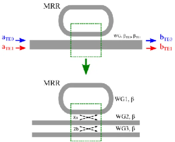
Ring-assisted modal conversion for on-chip mode-division multiplexing signal processing
Texte intégral
Figure
Documents relatifs
In this paper, we review techniques for biasing 2D time di- vision SQUID multiplexing: firstly, using bias resistors which adds power dissipation and cross talk; then,
The wide- spread use of a rotavirus vaccine could go a long way toward achieving the goals of world leaders who declared at the World Summit for Children (New York City, 1990)
We analyse the performance of such a reservoir on a classical nonlinear boolean task (the delayed XOR task) for (i) various designs of the reservoir in terms of lengths of
As seen in previous works, VFDM is highly dependent on perfect channel state information at the transmitter (CSIT) to be able to achieve zero interference at the primary system.
The output resolution of TDM HFB-based ADC is better than the classical one in the presence of realization errors of analysis filter bank. Besides, the TDM HFB architecture can
a) The design of two types of erbium doping profile for few-mode erbium-doped fiber that supports three spatial modes. The goal of the fiber design is to achieve modal gain
Molding press production is controlled by the floor space allocated to storage between molding and the bonding cell; some type of reorder point scheduling methodology for the
He finds that capex is positively correlated with NOI, property value, and building size, which is intuitively obvious, but that capex per square foot is negatively
