Developing Ultrasensitive and CMOS Compatible ISFETs in the
BEOL of Industrial UTBB FDSOI Transistors
A thesis submitted to Université de Sherbrooke and Université de Lyon (co-supervised) in
partial fulfillment of the requirements of the degree of Doctor of Philosophy
Getenet Tesega AYELE
Jury:
COHEN-BOUHACINA, Touria
Université de Bordeaux
Rapporteur
GUIDUCCI, Carlotta
EPFL
Rapporteur
CANVA, Michael
Université de Sherbrooke
Rapporteur
CLEMENT, Nicolas
Université de Tokyo
Examinateur
DROUIN, Dominique
Université de Sherbrooke
Directeur de thèse
SOUIFI, Abdelkader
INSA-LYON
Co-directeur de thèse
CLOAREC, Jean-Pierre
Ecole Central de Lyon
Invité
MONFRAY, Stephane
STMicroelectronics
Invité
ECOFFEY, Serge
Université de Sherbrooke
Invité
Lyon, France May, 2019
iii
Abstract
The sensor market has recently seen a dramatic growth fueled by the remarkable application of sensors in the consumer electronics, automation industry, wearable devices, the automotive sector, and in the increasingly adopted internet of things (IoT). The advanced complementary metal oxide semiconductor (CMOS) technology, the nano and micro fabrication technologies, and the innovative material synthesis platforms are also driving forces for the incredible development of the sensor industry. These technological advancements have enabled realization of sensors with characteristic features of increased accuracy, miniaturized dimension, integrability, volume production, highly reduced cost, and fast response time. Ion-sensitive field-effect transistors (ISFETs) are solid state (bio)chemical sensors, for pH (H+), Na+, K+ ion
detection, that are equipped with the promise of the highly aspired features of CMOS devices. Despite this, the commercialization of ISFETs is still at the stage of infancy after nearly five decades of research and development. This is due mainly to the limited sensitivity, the controversy over the use of the reference electrode for ISFET operation, and because of stability issues. In this thesis, ultrasensitive and CMOS compatible ISFETs are integrated in the back end of line (BEOL) of standard UTBB FDSOI transistors. A capacitive divider circuit is employed for biasing the front gate for stable performance of the sensor. Exploiting the intrinsic amplification feature provided by UTBB FDSOI transistors, we demonstrated ultrahigh sensitive ISFETs. The amplification arises from the strong electrostatic coupling between the front gate and the back gate of the FDSOI, and the asymmetric capacitances of the two gates. A change in voltage at the front gate appears at the back gate as an amplified shift in voltage. The amplification, referred to as the coupling factor (γ), is equal to the ratio of the gate oxide capacitance and the buried oxide (BOX) capacitance. Therefore, functionalizing the pH sensing at the front gate of FDSOI devices, the change in surface potential at the front gate is detected at the back gate amplified by the coupling factor (γ), giving rise to an ultrahigh-sensitive solid state chemical sensor.
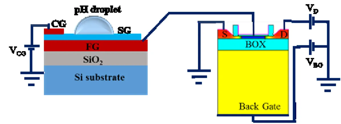
Integration of the sensing functionality was made in the BEOL which gives the benefits of increased reliability and life time of the sensor, compatibility with the standard CMOS process, and possibility for embedding a capacitive divider circuit. Operation of the MOSFETs without a proper front gate bias makes them vulnerable for undesired floating body effects. The capacitive divider circuit addresses these issues by biasing the front gate simultaneously with the sensing functionality at the same gate through capacitive coupling to a common BEOL metal. Therefore, the potential at the BEOL metal would be a weighted sum of the surface potential at the sensing gate and the applied bias at the control gate.
iv
The proposed sensor is modeled and simulated using TCAD-Sentaurus. A complete mathematical model is developed which provides the output of the sensor as a function of the solution pH (input to the sensor), and the design parameters of the capacitive divider circuit and the UTBB FDSOI transistor. In that case, consistent results have been obtained from the modeling and simulation works, with an expected sensitivity of 780 mV/pH corresponding to a sensing film having Nernst response.
The modeling and simulation of the proposed sensor was further validated by a proof of concept extended gate pH sensor fabrication and characterization. These sensors were developed by a separated processing of just the pH sensing component, which is electrically connected to the transistor only during characterization of the sensor. This provides faster and simpler realization of the sensor without the need for masks and patterning by lithography. The extended gate sensors showed 475 mV/pH sensitivity which is superior to state of the art low power ISFETs.
Finally, integration of the sensing functionality directly in the BEOL of the UTBB FDSOI devices was pursued. An experimental sensitivity of 730 mV/pH is obtained which is consistent with the mathematical model and the simulated response. This is more than 12-times higher than the Nernst limit, and superior to state of the art sensors. Sensors are also evaluated for stability, resolution, hysteresis, and drift in which excellent performances are demonstrated.
A novel pH sensing architecture is also successfully demonstrated in which the detection is functionalized at the gate protection diode rather than the front gate of UTBB FDSOI devices. The abrupt current switching, as low as 9 mV/decade, has the potential to increase the fixed bias sensitivity to 6.6 decade/pH. We experimentally demonstrated a sensitivity of 1.25 decade/pH which is superior to the state of the art sensitivity.
Key words—Back end of line (BEOL), capacitive coupling, CMOS, fully-depleted silicon-on-insulator (FDSOI), ion-sensitive field-effect transistor (ISFET), pH sensor, ultrathin body and buried oxide (UTBB)
v
Résumé
Le marché des capteurs a récemment connu une croissance spectaculaire alimentée par l'application remarquable de capteurs dans l'électronique de consommation, l'industrie de l'automatisation, les appareils portables, le secteur automobile et l'internet des objets de plus en plus adopté. La technologie avancée des complementary metal oxide semiconductor (CMOS), les technologies de nano et de micro-fabrication et les plateformes de synthèse de matériaux innovantes sont également des moteurs du développement incroyable de l'industrie des capteurs. Ces progrès ont permis la réalisation de capteurs dotés de nombreuses caractéristiques telles que la précision accrue, les dimensions miniaturisées, l’intégrabilité, la production de masse, le coût très réduit et le temps de réponse rapide.
Les ion-sensitive field-effect transistors (ISFETs) sont des capteurs à l'état solide (bio) chimiques, destinés à la détection des ions H+ (pH), Na+ et K+. Malgré cela, la commercialisation des ISFETs est encore à ses
balbutiements, après près de cinq décennies de recherche et développement. Cela est dû principalement à la sensibilité limitée, à la controverse sur l'utilisation de l'électrode de référence pour le fonctionnement des ISFETs et à des problèmes de stabilité. Dans cette thèse, les ISFETs ultrasensibles et compatibles CMOS sont intégrés dans le BEOL des transistors UTBB FDSOI standard. Un circuit diviseur capacitif est utilisé pour polariser la grille d’avant afin d'assurer des performances stables du capteur.
En exploitant la fonction d’amplification intrinsèque fournie par les transistors UTBB FDSOI, nous avons présenté des ISFET ultra sensibles. L'amplification découle du fort couplage électrostatique entre la grille avant et la grille arrière du FDSOI et des capacités asymétriques des deux grilles. Un changement de tension au niveau de la grille avant apparaît sur la grille arrière sous la forme d'un décalage amplifié de la tension. L'amplification, représentée par le facteur de couplage (γ), est égale au rapport de la capacité de l'oxyde de grille et de la capacité de le buried oxide (BOX). Par conséquent, en fonctionnalisant la détection du pH sur la grille avant pour les dispositifs FDSOI, la modification du potentiel de surface sur la grille avant est détectée par la grille arrière et amplifiée du facteur de couplage (γ), donnant lieu à un capteur chimique à l'état solide à sensibilité ultra-élevée.
L'intégration de la fonctionnalité de détection a été réalisée en back end of line (BEOL), ce qui offre les avantages d'une fiabilité et d'une durée de vie accrues du capteur, d'une compatibilité avec le processus CMOS standard et d'une possibilité d'intégration d'un circuit diviseur capacitif. Le fonctionnement des MOSFETs, sans une polarisation appropriée de la grille avant, les rend vulnérables aux effets de grilles flottantes indésirables. Le circuit diviseur capacitif résout ce problème en polarisant la grille avant tout en
vi
maintenant la fonctionnalité de détection sur la même grille par un couplage capacitif au métal commun du BEOL. Par conséquent, le potentiel au niveau du métal BEOL est une somme pondérée du potentiel de surface au niveau de la grille de détection et de la polarisation appliquée au niveau de la grille de contrôle. Le capteur proposé est modélisé et simulé à l'aide de TCAD-Sentaurus. Un modèle mathématique complet a été développé. Il fournit la réponse du capteur en fonction du pH de la solution (entrée du capteur) et des paramètres de conception du circuit diviseur capacitif et du transistor UTBB FDSOI. Dans ce cas, des résultats cohérents ont été obtenus des travaux de modélisation et de simulation, avec une sensibilité attendue de 780 mV / pH correspondant à un film de détection ayant une réponse de Nernst.
La modélisation et la simulation du capteur proposé ont également été validées par une fabrication et une caractérisation du capteur de pH à grille étendue avec validation de son concept. Ces capteurs ont été développés par un traitement séparé du composant de détection de pH, qui est connecté électriquement au transistor uniquement lors de la caractérisation du capteur. Ceci permet une réalisation plus rapide et plus simple du capteur sans avoir besoin de masques et de motifs par lithographie. Les capteurs à grille étendue ont présenté une sensibilité de 475 mV/pH, ce qui est supérieur aux ISFET de faible puissance de l'état de l’art.
Enfin, l’intégration de la fonctionnalité de détection directement dans le BEOL des dispositifs FDSOI UTBB a été poursuivie. Une sensibilité expérimentale de 730 mV/pH a été obtenue, ce qui confirme le modèle mathématique et la réponse simulée. Cette valeur est 12 fois supérieure à la limite de Nernst et supérieure aux capteurs de l'état de l’art. Les capteurs sont également évalués pour la stabilité, la résolution, l'hystérésis et la dérive dans lesquels d'excellentes performances sont démontrées.
Une nouvelle architecture de détection du pH est également démontrée avec succès, dans laquelle la détection est fonctionnalisée au niveau de la diode de protection de la grille plutôt que de la grille avant des dispositifs UTBB FDSOI. La commutation de courant abrupte, aussi basse que 9 mV/decade, pourrait potentiellement augmenter la sensibilité de polarisation fixée à 6,6 decade/pH. Nous avons démontré expérimentalement une sensibilité de 1,25 decade/pH supérieure à la sensibilité reportée à l’état de l’art.
Mots-clés: Back end of line (BEOL), couplage capacitif, CMOS, fully depleted silicon on insulator (FDSOI), ion-sensitive field-effect transistor (ISFET), capteur de pH, ultrathin body and buried oxide (UTBB)
vii
Table of Contents
Abstract ... iii Résumé ... v List of Figures ... xi List of Tables ... xvList of Abbreviations and Acronyms ... xvi
List of Symbols ... xix
Acknowledgement ... xxi CHAPTER ONE... 1 INTRODUCTION ... 1 1.1 pH Sensors ... 2 1.2 Context ... 5 1.3 Objective ... 6
1.4 Outline of the Thesis ... 7
CHAPTER TWO ... 10
LITERATURE REVIEW ... 10
2.1 Early Developments on ISFETs ... 10
2.2 Floating Gate ISFETs ... 13
2.3 Super Nernstian Sensitivity ISFETs ... 17
2.4 Nanowire, TFET and FinFET based ISFETs ... 21
2.5 BioFET Sensors ... 23
2.6 Backside Contact ISFETs ... 25
2.7 pH-Sensing Films ... 25
2.8 Drift and Hysteresis ... 27
2.9 The Reference Electrode ... 29
2.10 Conclusion ... 33
viii
MODELING AND SIMULATION ... 36
3.1 The EI Interface ... 37
3.2 The Capacitive Divider Circuit ... 41
3.3 UTBB FDSOI Devices ... 42
3.4 The pH Sensor with a Capacitive Divider Circuit ... 50
3.5 Simulation of the Sensor ... 52
3.5.1 Sensing the Surface Charge ... 53
3.5.2 Sensing the Surface Potential ... 55
3.6 Sensing at the Gate Protection Diode ... 58
3.7 Conclusion ... 62
CHAPTER FOUR ... 65
FABRICATION OF THE SENSORS ... 65
4.1 Layout of the Devices on the Die ... 65
4.2 The Proof of Concept Sensors ... 66
4.3 Integration of the Sensors in BEOL ... 68
4.3.1 Process Flow ... 68
4.3.2 Mask Design ... 71
4.3.3 Fabrication Process ... 74
4.4 Fabrication of Mixed-type Sensors on a Die ... 80
4.4.1 Process Flow ... 82 4.4.2 Mask Design ... 84 4.4.3 Fabrication Process ... 87 4.5 Conclusion ... 93 CHAPTER FIVE ... 95 CHARACTERIZATION ... 95 5.1 Figures of Merit ... 95 5.2 Characterization Protocol ... 99
ix
5.3 The Proof of Concept EG pH sensor ... 102
5.4 The Sensor Integrated in BEOL ... 105
5.5 Sensing at the Gate Protection Diode ... 115
5.6 Conclusion ... 118
CHAPTER SIX ... 120
CONCLUSION ... 120
6.1 Summary of the Thesis ... 121
6.1.1 Modeling and Simulation ... 122
6.1.2 EG pH Sensor ... 122
6.1.3 Sensor in BEOL of FDSOI ... 123
6.1.4 Sensing at Diode ... 123 6.2 Original Contribution ... 123 6.3 Perspective... 124 APPENDIX-I... 126 RÉSUMÉ ÉTENDU ... 126 A1. Introduction ... 126
A2. Etat de l'art ... 127
A3. Modélisation et simulation ... 132
A4. Capteur de pH EG ... 134
A5. Capteur en BEOL de FDSOI ... 136
A6. Détection à la diode ... 139
A7. Conclusion ... 142
APPENDIX-II ... 147
SIMULATION CODES ... 147
APPENDIX-III ... 150
MASKS USED FOR FABRICATION ... 150
x
PUBLICATIONS ... 158 References ... 160
xi
List of Figures
Figure 1. 1 Illustration of the internet of things and big data [GSMA, web] ... 1
Figure 1. 2 An Ag/AgCl glass electrode [12] ... 2
Figure 1. 3 Different components of sensors ... 3
Figure 1. 4 Structure of an ISFET ... 4
Figure 2. 1 Cross sectional view of the ISFET reported by P. Bergveld in 1970 ... 11
Figure 2. 2 Schematic diagram of the ISFET reported by Matsuo and Wise in 1974 ... 12
Figure 2. 3 Schematic diagram of floating gate ISFET ... 14
Figure 2. 4 Diagram of sensor used for DNA sequencing [59] ... 16
Figure 2. 5 Schematic diagram of the ISFET reported by [74] ... 17
Figure 2. 6 Schematic diagram of the SiNW/CMOS hybrid ISFET [75] ... 18
Figure 2. 7 Sensitivity scaling with capacitance ratio and schematics of the dual gate ISFET [76] ... 19
Figure 2. 8 Schematic diagram of dual gate SOI ISFET with a back-side sensing [78] ... 20
Figure 2. 9 Silicon nanowire (SiNW) chemical sensor [97] ... 22
Figure 2. 10 Schematics of a penicillin-sensitive EnFET (PenFET) [116] ... 23
Figure 2. 11 pH sensitivities of ISFETs having different sensing films [39] ... 26
Figure 2. 12 Long term drift as a function of temperature [139] ... 28
Figure 2. 13 pH dependent drift in amorphous tungsten oxide [40] ... 29
Figure 2. 14 Schematic diagram of the sensor with interdigitated architecture [70] ... 31
Figure 2. 15 Schematics of a supercapacitor (C1 and C2 stand for capacitances) [164] ... 32
Figure 2. 16 Illustration of electro-osmosis [166] ... 33
Figure 3. 1 The electrical double layer. ... 38
Figure 3. 2 Schematic diagram of the capacitive divider circuit (left), and its equivalent circuit (right) .... 41
Figure 3. 3 Cross section of the UTBB FDSOI transistor ... 42
Figure 3. 4 Schematic diagram of industrial n-type flip-well UTBB FDSOI transistors ... 43
Figure 3. 5 The electrical connection diagram for characterization of the electrostatic coupling between the front gate and the back gate (NFET SLVT) ... 45
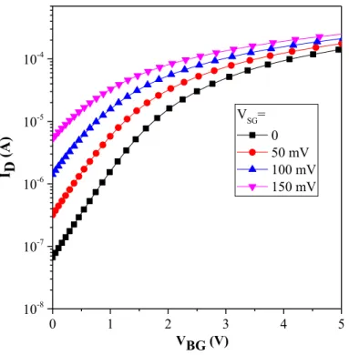
Figure 3. 6 Measured ID-VBG characteristics of the UTBB FDSOI devices ... 45
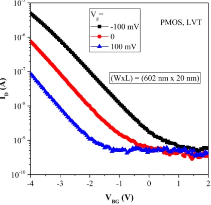
Figure 3. 7 Measured ID-VBG characteristics of the LVT PFET UTBB FDSOI device ... 46
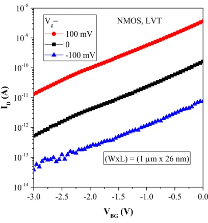
Figure 3. 8 Measured ID-VBG characteristics of LVT NFET UTBB FDSOI devices ... 47
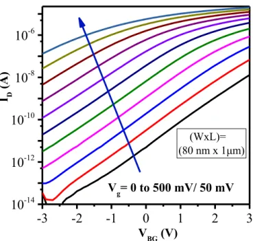
Figure 3. 9 Attenuated shift in threshold voltage at the front gate induced by a change in back gate voltage ... 48
xii
Figure 3. 10 Tuning of the linear operating regime to the left (negative VBG) for higher potentials at the
front gate. ... 49
Figure 3. 11 Tuning of the linear operating regime to the right for negative potentials at the front gate ... 50
Figure 3. 12 Schematics of the pH sensor integrated in BEOL of UTBB FDSOI (left) and its equivalent electrostatic model (right) ... 50
Figure 3. 13 Potential profile (left), charge distribution (middle), and major parameters (right) of the simulated sensor ... 53
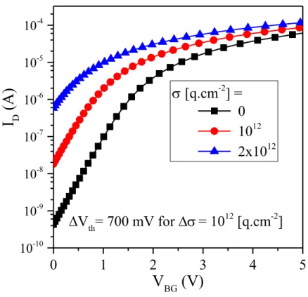
Figure 3. 14 Simulated ID-VBG characteristics of the FDSOI ISFET at different surface charges at the sensing gate (SG)... 54
Figure 3. 15 Simulated ID-VBG characteristics of the FDSOI ISFET at different surface potentials at the sensing gate (SG)... 56
Figure 3. 16 Simulation result showing reduced sensitivity at comparable dimensions of the sensing gate capacitor. ... 57
Figure 3. 17 Simulation result showing no response to change in control gate voltage. ... 58
Figure 3. 18 Schematic diagram of the sensor in which sensing is made at the gate protection diode. ... 58
Figure 3. 19 Schematics of the sensor with FDSOI and NPN connection. ... 59
Figure 3. 20 Drain current switching due to the DIBL effect ... 59
Figure 3. 21 Dependence of the DIBL effect on device gate length ... 60
Figure 3. 22 Dependence of the DIBL effect on drain voltage ... 61
Figure 3. 23 Simulation result showing the potential distribution in short UTBB FDSOI devices. ... 61
Figure 3. 24 Shift of the ID-VBG curve depending on the diode bias ... 62
Figure 4. 1 Layout of the block of transistors on the (2.5 cm x 2.9 cm) die ... 65
Figure 4. 2 Schematic diagram of the proof of concept extended gate pH sensor ... 67
Figure 4. 3 SEM cross sectional image of the transistors. ... 68
Figure 4. 4 XPS characterization of ALD deposited aluminum oxide ... 69
Figure 4. 5 Process flow for integration of the pH sensors in the BEOL [199] ... 70
Figure 4. 6 Top down schematic diagram of the sensor ... 71
Figure 4. 7 Overall layout of the mask ... 72
Figure 4. 8 Optical measurement of the dimensions and spacing of the pads at 20X (left) and 50X (right) magnifications ... 73
Figure 4. 9 Layout and dimensions of the sensing gate and the control gate ... 73
Figure 4. 10 Optical image of the sensor after UV-1: opening for S, D, G, BG pads ... 75
xiii
Figure 4. 12 Optical image of the sensor at the end of Ti/Al deposition and patterning (SG is the sensing
area, also called sensing gate; CG is the control gate) ... 78
Figure 4. 13 SEM cross sectional image of the sensor ... 79
Figure 4. 14 outline of the fabricated sensors, with the optical image as an inset and a pH droplet dispensed on the sensing area [38] ... 80
Figure 4. 15 The modified dicing scheme to place the block of transistors at the center of the die ... 81
Figure 4. 16 The selected rows of transistors (left), and outline of sensors on the surface of the die (right) ... 82
Figure 4. 17 Process flow indicating the integration of pH sensor in the BEOL. ... 83
Figure 4. 18 Process flow indicating fabrication of the pH sensor with extended sensing area ... 84
Figure 4. 19 Overall outline of the mask ... 85
Figure 4. 20 Layout of the control gate and sensing gate of BEOL integrated sensors (red: control gate, black: sensing area) ... 86
Figure 4. 21 The control gate design of the extended gate sensors ... 87
Figure 4. 22 Optical image of the sample after pad opening (UV-1) ... 88
Figure 4. 23 Optical image of the sample after UV-2 for metallic extension ... 89
Figure 4. 24 XPS characterization of the aluminum oxide deposited by sputtering ... 90
Figure 4. 25 Optical image of the sensor after control gate deposition and patterning (UV-4) ... 91
Figure 4. 26 Top down SEM image of the mixed type sensors in the vicinity of extended sensing areas .. 92
Figure 4. 27 Top down SEM image of the mixed type sensors in the vicinity of electrical contacts ... 92
Figure 5. 1 The characterization bench ... 95
Figure 5. 2 Calibration curve of a sensor [205] ... 96
Figure 5. 3 Illustration of accuracy and precision using analogy with game of darts [210]... 98
Figure 5. 4 Illustration of hysteresis behavior of a sensor [205] ... 99
Figure 5. 5 pH sensitivity of the extended gate pH sensor ... 103
Figure 5. 6 Repeatability of the ID-VBG characteristics of the extended gate sensor at pH 8 ... 104
Figure 5. 7 Chronogram of the extended gate pH sensor’s response ... 104
Figure 5. 8 Stability characterization with and without a bias at the control gate ... 105
Figure 5. 9 Sensitivity of the BEOL integrated pH sensors ... 106
Figure 5. 10 Modulation of the BEOL integrated pH sensors’ output through control gate ... 107
Figure 5. 11 Chronogram of the BEOL integrated sensors’ response ... 107
Figure 5. 12 pH response of sensors, before (left) and after (right) normalization function, with drain leakage current through cured AZ-1512 resist ... 108
xiv
Figure 5. 13 Measured currents of the pH sensor through the drain, source, control gate and back gate in
dry condition... 109
Figure 5. 14 Measured currents of the pH sensor through the drain, source, control gate and back gate in pH 10 ... 110
Figure 5. 15 Measured pH response of sensors developed based on p-type FDSOI devices ... 111
Figure 5. 16 Attenuated sensitivity of a pH sensor ... 111
Figure 5. 17 Response time of the BEOL integrated sensors ... 112
Figure 5. 18 Diagram showing the response for resolution computation of the BEOL integrated sensors113 Figure 5. 19 Diagram showing the hysteresis of the BEOL integrated sensors ... 114
Figure 5. 20 Measured response of the sensor for drift study ... 114
Figure 5. 21 pH response at lower drain voltage (VDD=0.1 V) ... 115
Figure 5. 22 Sensitivity and linearity of pH response at lower drain voltage (VDD=0.1 V) ... 116
Figure 5. 23 pH response at higher drain voltage (VDD=0.6 V) ... 116
Figure 5. 24 pH response of short devices ... 117
Figure 5. 25 Chronogram of sensors based on very short devices ... 117
Figure 6. 1 Sensitivity benchmark of the sensor for fixed current readout ... 120
xv
List of Tables
Table 2. 1 Hysteresis results of different sensing films [143] ... 28
Table 3. 1 Calculated changes in floating gate voltage for different changes in control gate voltage ... 57
Table 4. 1 Deposition recipe of the ALD aluminum oxide ... 74
Table 4. 2 Photolithography process with AZ1512 photoresist ... 76
Table 4. 3 Deposition recipe of Ti/Al deposition by sputtering ... 77
xvi
List of Abbreviations and Acronyms
ALD Atomic Layer Deposition
BEOL Back End of Line
BG Back Gate
BOX Buried Oxide
cm Centimeter
CMOS Complementary Metal Oxide Semiconductor
CVD Chemical Vapour Deposition
DG Dual Gate
DG ISFET Dual Gate Ion-Sensitive Field-Effect Transistor
DI Deionized
DIBL Drain Induced Barrier Lowering
DL Double Layer
EDL Electrical Double Layer
EG Extended gate
EI Electrolyte-Insulator
EIS Electrolyte Insulator Semiconductor
fA Femtoampere
FDSOI Fully Depleted Silicon on Insulator
FET Field-Effect Transistor
FEOL Front End of Line
FG Floating Gate
FG ISFET Floating Gate Ion-Sensitive Field-Effect Transistor FinFET Fin Field-Effect Transistor
GP Ground Plane
IC Integrated Circuit
ILD Inter Layer Dielectric
IMOS Impact Ionization Metal Oxide Semiconductor Field-Effect Transistor
IoT Internet of Things
IPA Isopropanol
IR Infrared
ITRS International Technology Roadmap for Semiconductors
xvii
min Minute
MIS Metal Insulator Semiconductor
mm Millimeter
MOS Metal Oxide Semiconductor
MOSFET Metal Oxide Semiconductor Field-Effect Transistor
mV Millivolt
NFET N-channel Field-Effect Transistor
nm Nanometer
NMOS Negative Channel Metal Oxide Semiconductor
NW Nanowire
NWFET Nanowire Field-Effect Transistor
PFET P-channel Field-Effect Transistor
PMMA Poly(methyl methacrylate)
PMOS p-type Metal Oxide Semiconductor
PVC Polyvinyl chloride
PVD Physical Vapor Deposition
REF Reference Electrode
REFET Reference Field-Effect Transistor
RF Radio Frequency
RIE Reactive Ion Etching
SBFET Schottky Barrier Field-Effect Transistor
SCE Short Channel Effect
SEM Scanning Electron Microscope
SG-FET Suspended Gate Field-Effect Transistor
SiGe Silicon Germanium
SiNW Silicon Nanowire
SLVT Super Low Threshold Voltage
SNR Signal to Noise Ratio
SoC System on Chip
SOI Silicon on Insulator
SS Subthreshold Swing
SW-CNT Single Walled Carbon Nanotube
TFET Tunnel Field-Effect Transistor
xviii
UTBB Ultrathin Body and BOX
UV Ultraviolet
xix
List of Symbols
α pH Buffer Capacity
σ Surface Charge Density
∆V Change in Voltage kB Boltzmann Constant µA Microampere µl Microliter µm Micrometer µs Microsecond µV Microvolt φ Surface Potential γ Coupling Factor A Ampere A Area C Coulomb
CBOX BOX Capacitance
CCG Capacitance of Control Gate
COX Gate Oxide Capacitance
CSG Capacitance of Sensing Gate
CT Total Capacitance D Drain f Femto F Farad G Gate I Current L Length m Milli m Meter n Nano q Elementary Charge Q Charge s Second S Source
xx S Subthreshold Slope Si Silicon t Time T Temperature V Voltage
VBG Back Gate Voltage
VCG Control Gate Voltage
Vg Gate Voltage
VSG Sensing Gate Voltage
xxi
Acknowledgement
I am very thankful to my thesis supervisors Abdelkader SOUIFI, Dominique DROUIN and Jean-Pierre CLOAREC for their advice, guidance and help throughout the three years of my PhD study. My sincere gratitude goes also to Stephane MONFRAY and Serge ECOFFEY whose contribution is huge for the successful completion of this research work.
Special thanks is for Juliana CHAWICH. I would also thank students and colleagues at ST Crolles, INL and 3IT, with whom my stay was enjoyable. I generally thank all the people who contributed to this work one way or another.
I would like to thank the examiners and all the jury members of this PhD defense for their precious time. Last but not least, many thanks to STMicroelectronics for their generous financing of this PhD thesis through a CIFRE program.
1
CHAPTER ONE
INTRODUCTION
The modern age marks the beginning of the fourth industrial revolution (Industry 4.0) which is characterized by the integration of the computing network and the physical world (cyber-physical system), commonly referred to as the internet of things (IoT) [1]–[4]. Artificial intelligence (AI), big data, machine learning, and deep learning are the other emerging technologies constituting the majority of the technological developments of the near future [5], [6]. Sensors form the corner stone of all these technologies ensuring the data streaming from the physical world to the computing network.
Figure 1. 1 Illustration of the internet of things and big data [GSMA, web]
In broader terms, the essence of sensors goes as far as the very existence of living things as it is through biological sensors that cells, organs and organisms function in a healthy metabolic condition, and toxic free environment. Such sensors detect or measure oxygen level, hormones, nutrients, light, motion, temperature, toxins, and other internal and environmental chemical, bio, and physical property. Other than the biological sensors, we use sensors in our daily lives ranging from the traditional temperature and touch sensitive devices to more sophisticated smart objects.
The sensor market has recently seen a dramatic growth fueled by the remarkable application of sensors in the consumer electronics, automation industry, wearable devices, the automotive sector, and the increasingly
2
adopted internet of things (IoT) [1], [7]. It is also driven by innovative material synthesis and processing along with fabrication technologies such as complementary metal oxide (CMOS) and micro electromechanical systems (MEMS) [8], [9]. These advanced technologies enabled development of sensors with characteristic features of increased accuracy, miniaturized dimension, highly reduced cost, and fast response time.
The global sensor market is forecasted to grow exponentially at a compound annual growth rate (CAGR) of 11.3 % during the period 2016 – 2022, reaching $241 billion by 2022 [8]. The worldwide IoT market which encompasses not only the sensors but also the connectivity equipments and IoT platforms, is on the other hand predicted to grow at a 20% CAGR hitting $7.1 trillion in 2020 [10], [11].
1.1 pH Sensors
Glass electrode, the first chemical sensor ever developed, is a pH sensor which is the most widely used equipment for acidity measurement [9]. Nevertheless, it has severe limitations such as bulky size, fragility, toxicity (in the case of saturated calomel electrode), and CMOS incompatibility. In addition, large volume of sample is required for pH testing with glass electrodes. Acidity measurement in food processing plants is risky with glass electrodes─ if the fragile instrument breaks, the whole inventory in the process line would be thrown away due to strict quality control and security requirements. pH measurement of soil requires rugged instruments due to the harsh environment. Miniaturized sensors can also be hardly met with the glass electrode. Basic components of an Ag/AgCl electrode are shown on figure 1.2.
3
The alternative pH measuring mechanisms involve optical [13]–[16], acoustic [17], magnetic [18], [19], MEMS [20], light addressable potentiometric sensing (LAPS) [21]–[24], and field-effect transistor [25], [26] detection or transduction methods. Figure 1.3 shows the block diagram of the reception, transduction, and signal processing stages of such sensors. The optical pH sensors are based on the shift in photonic absorption spectrum depending on the pH value, while the change in velocity of surface acoustic waves is used for acoustic pH sensors. In the cases of magnetic and MEMS pH sensors, the change in vibration speed and deflection of the microcantilever respectively are recorded for the pH sensing. The electronic pH sensing techniques, LAPS and ISFET, rely on a pH dependent shift in potential.
Figure 1. 3 Different components of sensors
ISFETs (ion-sensitive field-effect transistors) are solid state ion sensors in which the drain current is modulated by the ion activity of an aqueous solution. The schematic diagram of the basic ISFET structure is shown on figure 1.4. Such CMOS chemical sensors provide immense benefits over the other pH sensing alternatives. Some of the benefits are the high input impedance, dc and low frequency bandwidth, small size, reliability, fast response time, and multi-sensor chip [26], [27]. They also enable on-chip signal processing to achieve high to low impedance transformation, temperature compensation, and signal multiplexing [27]. In addition, they are useful for in situ impedance transformation, relatively easy possibility of manufacturing small and rugged multi-probes [28]. MOS based sensors have also the potential to detect minute traces of charge, 1010 charges/cm2, or few tens of charges in a device of 1 µm by 100 nm
4
Figure 1. 4 Structure of an ISFET
The global pH sensor market is predicted to gain an exponential growth, at ~4% of a CAGR during 2017 - 2023, reaching $1.8 billion in 2023 [30]. This market of the pH sensors range from consumer use drink water acidity/alkalinity monitoring to large scale industrial process controls. Below is a list of the main potential industries deploying the largest share of pH sensors.
The ever increasing world population, the highly rising rate of urbanization and industrialization, the alerting climatic change all call for wider use of pH sensors for tighter monitoring of water pH and wiser use of the depleting water resource [30]. The advanced CMOS technology and nanotechnology are also driving forces towards providing affordable solutions for end user water quality measurement systems which in turn widens the market of these sensors. Therefore, water acidity measurement both at central water treatment plant level and end user level, is a big future market for the pH sensors.
Agriculture is one of the fore front industries to be boosted by the fourth industrial revolution- the internet of things. This is through continuous data collection, automation and fast decision making. pH sensors play a key role in such smart agriculture by providing data on soil acidity and pH value of the rain water. The rugged nature of solid state pH sensors is also suited for soil acidity measurement in the harsh environments of farming fields.
Pharmaceuticals, and chemical industries in general, can control quality of their products and monitor their fabrication processes using pH sensors. Correlating the pH value of the semi product with its process step, application of these sensors help for monitoring of industrial processes. Acidity measurement of chemicals in chemical research laboratories is also a big market for these sensors.
5
controlling quality of products. Acidity level of the food or drink indicate not only the planned processing of the semiproduct, but also the compatibility of the intake with the user’s health condition.
The health industry, which takes the lion’s share of the overall global market, is not an exception for wide use of pH sensors. The humans’ body fluids such as the gastric juice, intestinal fluid, urine, blood, saliva, and sweat carry ample amount of information about the health condition of the person. Therefore, pH sensors are applicable in the health industry for collecting data about the person’s health.
1.2 Context
Integrating ultrasensitive pH sensors in the BEOL of industrial UTBB FDSOI devices, the context of this research can be presented from several dimensions. The main points of interest are the miniaturization and the ruggedness provided by the solid state sensor over the widely used glass electrode, the signal amplification in FDSOI transistors, the biasing functionality of the capacitive divider circuit, the benefits provided by the BEOL integration, and the advantages of developing sensors based on industrial devices. Acidity measurement with glass electrodes does not meet the requirements of several industries. The fragile nature of the glass makes the instrument a less attractive option in agriculture and food processing industries. The big dimension of this device is a constraint towards implantables and small test-volume applications. These and other limitations of the contemporary technology, and the potential attractive features of the highly advanced CMOS technology led to intensive investigation of the solid state solution- the ISFETs. The commercialization of ion-sensitive field-effect transistors, solid state pH sensors, is still at the stage of infancy after nearly 5-decades of research and development. This is due mainly to the constraint imposed by the use of reference electrode. The miniaturized solid state sensor operated with a large reference electrode does not allow to exploit the potential attractive features of ISFETs. Consequently, operation of such sensors without reference electrode provides full exploitation of the long aspired advantages of the highly matured CMOS technology.
Several times, development of certain technological solutions are driven not only by demands but also opportunities provided by complementing technological advancements. The introduction of UTBB FDSOI devices is not an exception to this trend that such device architectures provide special features for sensing applications. Although these FDSOI transistors were developed mainly for logic applications, the strong electrostatic coupling between the front gate and back gate of FDSOI provide an intrinsic amplification
6
feature for sensing applications enabling fabrication of ultrasensitive sensors.
When an MOSFET is operated without a bias applied to the front gate (electrically floating), its potential is determined by stochastic factors such as trapped charges and potentials coupled through parasitic capacitances [31]. The presence of peak doping near the back interface, for the ground plane of SOI devices, introduces existence of neutral region in the film which in turn results in floating body effect [32]. This kind of device operation results in instabilities in drain current and threshold voltage. It may also result in formation of a parasitic bipolar transistor in the MOS structure, which creates impact ionization and reduced drain breakdown voltage [33]. It can also cause anomalous I-V characteristics, transients, and hysteresis [33]. Despite the presence of all the above listed problems, most of the ISFETs reported on literature do not have effective front gate biasing connection. Therefore, a mechanism such as a capacitive divider circuit should be employed in ISFETs to enable both sensing and biasing functionalities at the front gate of the transistor.
Noise has been mentioned in several literature reports of solid state pH sensors as one of the main bottlenecks. However, the exact sources of such noises have not been well investigated, except some intuitive anticipations that the noise arises from the electrolyte-insulator interface. Nevertheless, transistors alone that are fabricated by non-standard processes can give I-V characteristics of relatively high variability and noise. Indeed, in [34] it is reported that the ISFET noise is dominated by the FET transistor noise. Thus, developing pH sensors based on industrial transistors is an excellent approach for developing sensors that have highly reduced noise levels.
Summarizing the discussion, the context of this work encompasses surpassing the Nernst limit of pH sensitivity employing UTBB FDSOI transistors, enabling stable performance of the sensor by applying a front gate bias through a capacitively coupled control gate, and ensuring CMOS compatibility by substituting the conventional reference electrode by a simple capacitive divider circuit. Last but not least, the BEOL integration helps to achieve volume production of the sensors with the advanced CMOS platform, and provides better life time for the sensors.
1.3 Objective
The general objective of this PhD thesis is to demonstrate integration of ultrasensitive and CMOS compatible pH sensors in the BEOL of industrial UTBB FDSOI devices. Such goal of integration encompasses the following specific objectives.
7
• To demonstrate ultrasensitive pH sensors exploiting the special features of UTBB FDSOI transistors,
• To enable CMOS compatibility of the sensors replacing the reference electrode with a capacitively coupled control gate,
• To employ a capacitive divider circuit at the front gate for sensing and front gate biasing simultaneously,
• To functionalize the sensing film on top of the BEOL gate metal, and • To pursue the signal recording at the back gate.
The above mentioned general and specific objectives encompass experimental demonstration and validation through modeling. More specifically, this includes the following major tasks:
• Mathematical modeling, • TCAD simulation,
• Proof of concept demonstration, and
• Final prototype fabrication and characterization.
1.4 Outline of the Thesis
This thesis is organized into 6-chapters. The first chapter is introduction of the research topic in which the overall review of the sensors, the market trend and applicability of the pH sensors, the context of the research work, the open research question, and the objectives are described.
The second chapter comprises the literature review in which a brief history and developmental research works on the solid state pH sensor are presented. Major reports on modifications of the sensor architectures, derivatives of the ISFETs, sensors based on recent transistor technologies, explored ion sensing materials, and non-idealities in ISFETs are highlighted. Analysis and comparison are also provided on the state of the art sensors to indicate the pros and cons of the different approaches.
Modeling and simulation work of the proposed sensor is presented in the third chapter. This chapter consists of a rigorous modeling and analysis of the different components of the sensor, mainly the FDSOI transistor, the capacitive divider circuit, and the electrolyte-insulator interface. TCAD simulation is also included to endorse the mathematical model of the sensor.
8
mask design, the layout of the transistors and sensors on the die, the process flow, and each fabrication process step are discussed in this chapter. It includes discussion of fabrication processes of the extended gate sensor, the sensor integrated in the BEOL, and the mixed-type sensors.
The fifth chapter provides the experimental result and discussion part of the project. This characterization chapter starts with a concise description of the parameters (figures of merit) used for evaluation of the sensors’ performances, followed by a description of the protocols employed for measurement of each figure of merit. Finally, the experimentally measured performances of the extended gate and the BEOL integrated sensors are provided. Results of sensors’ performances while sensing through the gate protection diode are also presented in the last section of this chapter.
At last, a concise summary of the thesis is provided on the sixth chapter. Summarizing the core points of the research work, the major original contributions and the perspectives suggested for future work are mentioned in this last chapter.
10
CHAPTER TWO
LITERATURE REVIEW
Solid state ion sensors, that are also commonly called ion-sensitive field-effect transistors (ISFETs), have received extensive research and development since their first invention in 1970 [25]. After nearly 5-decades of research, they are still at their stage of infancy towards commercialization due mainly to the limited sensitivity, the reference electrode, and stability issues [35]–[38]. In this chapter, we review and analyze the major literature reports on different aspects of such sensors that are published since the first inception of FET based ion sensors.
2.1 Early Developments on ISFETs
In 1970, P. Bergveld reported the ion-sensitive field-effect transistor, in which he explained the possibility of modulating the drain current through the double layer that is formed at the electrolyte-oxide interface [25]. Removing the gate metal of the MOSFET, he exposed the gate oxide of the transistor to an aqueous solution to probe the molar concentration of sodium ion (Na+) in the electrolyte (schematic diagram is shown
on figure 2.1). Without use of reference electrode, a linearly increasing drain current was demonstrated as a function of logarithmic molar concentration of sodium chloride (NaCl).
The motivation came from the observation that recording of ion activities in electrochemical and biological environments through measurement of potential differences between two electrodes suffers from noise contributed by several non-specific phenomena. According to Bergveld, this can be mitigated through probing of the local surface charge density at the interface of a double layer [25]. From the MOSFET theory that the threshold voltage (Vth) changes depending on trapped charges at the Si-SiO2 interface, such Vth
modulation can be obtained due to double layer charges arising from exposure of the gate oxide to the electrolyte. Exploiting this, a solid state ion sensor can be developed by immersing the gate oxide of an MOSFET into the electrolyte and monitoring the drain current.
11
Figure 2. 1 Cross sectional view of the ISFET reported by P. Bergveld in 1970
This work is impressive as a first demonstration of an MOSFET based chemical sensor. However, the short communication didn’t include sufficient explanation of repeatability, reliability, stability and selectivity so that this work received lots of criticisms especially from the perspective of the reference electrode. Use of silicon oxide as a sensing film is also another drawback of that work as this material is poorly selective and unstable [39], [40].
Two years later (in 1972), the inventor of the ISFET published his work on measurement of Na+ and H+ ion
activities employing field-effect device without use of reference electrode for the sensor operation [41]. In this work also, he emphasized on probing of the local electric field rather than the overall potential difference between the two electrodes. Nevertheless, an erroneous principle of operation is provided by making an analogy with that of a glass electrode. Such operation of ISFETs which is based on ion exchange of hydrated gel has later been proved incorrect by using non-hydrating materials such as silicon nitride as pH sensing layer.
Basing their work as later development of microelectrodes, Matsuo and Wise reported in 1974 a slightly modified ISFET [26]─ having a reference electrode, and silicon nitride (Si3N4) pH sensing film on top of
the gate oxide (SiO2). Consequently, they applied a bias through the reference electrode for their device
operation. The schematics is as shown below on figure 2.2. Although the use of silicon nitride as pH sensing material is better than silicon oxide, the use of the reference electrode has been an issue of controversy to date. Besides, the use of the conventional reference electrode restricts the attractive features of the CMOS chemical sensors such as small size, fast response time, and cheaper and volume production.
12
Figure 2. 2 Schematic diagram of the ISFET reported by Matsuo and Wise in 1974
On a review paper by JN Zemel, in 1975, operation of sensors without the reference electrode has been endorsed by justifying the principle of operation of the sensors with the observed threshold voltage shift of MOSFETs induced by oxide charges. Thus, he described the possibility of modulating the inversion layer as a function of in-diffusion of ions or out-migration of charges to the EI interface [42]. Although this paper described better the overall principle of operation of the sensors, the ion-diffusion based pH sensing mechanism accepted at that time is proved wrong later, following the introduction of site binding model by D. Yates, et al [43].
In the same year (1975), SD Moss et al developed a potassium sensitive solid state device using a valinomycin/plasticizer/poly(vinylchloride) membrane placed over the gate region of a field-effect transistor [44]. Although the principle of operation described resembles that of Bergveld’s analysis, measurements were made applying a bias through an Ag/AgCl reference electrode. In addition to the use of reference electrode, stability, reliability, repeatability and response time were not satisfactory in this work. Besides the components and architectures of the ISFETs, different materials have also been explored for usage as pH sensing material. At the end of the 1970s, T. Matsuo and M. Esashi published their work on pH sensing characteristics of different materials [45]. Even though they used LPCVD for the deposition (at around 800°C which is not compatible with some of the state of the art BEOL CMOS processes), their characterization of silicon oxide (SiO2), silicon nitride (Si3N4), aluminum oxide (Al2O3), and tantalum oxide
(Ta2O5) was very important. From this work, we could observe the poor performance of silicon oxide (in
terms of both sensitivity and selectivity) and the instability of silicon nitride, for pH sensing. On the contrary, aluminum oxide and tantalum oxide have near-Nernstian sensitivities (53 - 57 mV/pH) and very good selectivities (2 mV for Na+ and K+ ions) [45]. This work is very useful from the point of view of comparing
13
developed based on conventional bulk MOSFET, and since calomel reference electrode was used for front gate biasing.
Not so long after the invention of the ISFET, the instability of SiO2 and Si3N4 sensing films have been
studied by RM Cohen et al, in 1978 [46]. Intrigued by previous literature reports on instability of SiO2
sensing films due to hydration or gel formation at its surface [47], they studied the reliability of SiO2 and
Si3N4 sensing films. They attributed the earlier breakdown of SiO2 films due to microcrack formation,
recommending Si3N4 to be better sensing dielectric than SiO2.
SD Moss et al (1978), reported hydrogen, calcium, and potassium sensitive FET transducers in which Si3N4
is used as hydrogen ion sensing film while PVC membranes loaded with liquid ion exchangers (dodecyl phosphonate for calcium, valinomycin for potassium) and solution cast were employed for calcium and potassium ion sensing [27]. Near Nernstian responses and fast response times have been reported although the operation included use of reference electrode. The reported pH sensing performance was also limited in a narrow range, and small sensitivity compared to the Nernst response. The demonstrated sensitivity plot of the drain current vs pH is linear which is another limitation of the report compared to the state of the art semi-log response in the subthreshold regime.
To summarize, tens of publications have been made on ISFETs during the first decade from its first invention. These early research works emphasized on performance comparison among a few sensing films, and on demonstration of detecting different cations, such as Na+, K+, and Ca++. A few attempts on
elaboration of the principle of operation of the ISFET have also been made. The work from the perspective of exploring different pH sensing materials was successful as near Nernstian responsive dielectrics such as aluminum oxide and tantalum pentoxide have been reported.
2.2 Floating Gate ISFETs
Starting from the 1980s, the sensitive film could also be integrated on top of a floating gate metal, giving rise to either of a floating gate (FG) or an extended gate (EG) ISFET. This provides better isolation of the electronics part from the hostile liquid environment, helps further miniaturization [48], and is suited for easier sensor encapsulation. It also provides the opportunity for capacitive divider circuit where front gate biasing voltages and sensing-film surface potential can be capacitively-coupled to the common floating gate metal. The schematics of floating gate ISFET is shown below on figure 2.3.
14
Figure 2. 3 Schematic diagram of floating gate ISFET
A. K. Covington, et al., patented the extended gate ISFET in 1984, labelling it as “offset-gate chemical-sensitive field-effect transistor” [49]. They pointed that their invention is a development of the ion-selective-electrode (ISE), which is basically based on an extended conductor. The sensor was claimed to be applicable for detection and measurement of ion activity and concentration [50]. Although it was a great step towards promoting the floating gate ISFET architecture, this specific device was not effective compared to the state of the art BEOL integrated floating gate ISFET. Moreover, it does not have the gate biasing functionality. J Spiegel, et al., have developed a multi-species microprobe using extended gate chemically sensitive field-effect transistor [51]. Structure of this sensor consistes of a coaxial line which is an extension of the gate metal of the transistor. Depositing IrOx, AgCl and LaF3 thin films on the extended gate, they reported a
solid state sensing of H+, Cl-, and F- ions respectively. Unfortunately, their device’s sensitivity was very
small (less than 50 mV/pH), and the setup lacks front gate biasing.
L. Bousse, et al., have also published their works on floating gate ISFET, following the standard 2-µm CMOS process, which is modified only starting from the metal interconnect step [52]. With this work, they demonstrated the feasibility of fabricating ISFETs and associated circuits with a standard CMOS process with small modifications. As in the standard CMOS process, they used a polysilicon gate as a floating gate metal which was also used to define the source and drain regions. It was in turn covered with an LPCVD deposited silicon nitride which served as the pH-sensitive layer. Despite such CMOS compatible fabrication of the ISFET, this work had the limitations of front-gate biasing, limited sensitivity, and less-performing pH-sensing material (silicon nitride).
J. Bausells et al (1999) also reported pH sensing ISFETs developed on the second metal layer of standard CMOS [53]. Therefore, the sensor consisted of a floating electrode of the polysilicon and two metal layers on top of which an oxynitride layer exists serving as a pH sensing material. The use of standard CMOS
15
process helped them integrate the signal processing circuitry along with the ISFET on the same die. The floating gate architecture was crucial for the integrated sensor fabrication as the polysilicon was required for defining the source and drain (self-aligned) regions of the standard MOS device. The presence of the electrically floating polysilicon layer on the gate region had an additional benefit of reduced light sensitivity. In 2003, A. Minch et al., published their work on FET-based sensors based upon chemoreceptive neuron MOS transistor which was the combination of chemicapacitors, and neuron MOS ( MOS) transistors, with an extended floating gate structure for molecular and chemical sensing [54]. Mentioning the possibility of fabricating their sensor by a simple post-processing of conventional CMOS integrated circuits, they also pointed that the MOS area of their ISFET had very similar fabrication requirements to those of commercial Flash EEPROM, in which the FG is primarily adapted for nonvolatile storage. They emphasized, their work on the FG ISFET to be based on the characteristic feature of the floating gate MOS transistor that such devices can be constructed with any number of control-gate electrodes, which couple into the FG capacitively. The floating gate voltage is then established through charge sharing or capacitive voltage addition, as a weighted sum of the voltages that are applied at the control gates (CGs). The coefficient of each input signal is directly proportional to the capacitance of the corresponding control gate or sensing gate, and is normalized by the total capacitance seen by the floating gate. But their work uses the control gate for signal recording, which highly attenuates the sensitivity of the ISFET.
A. Cohen et al (2004) reported the recording of neuron activity using depletion mode floating gate ISFET developed by a post processing of 0.5 µm standard CMOS technology [55]. They pointed that the floating gate approach is preferable to protect the most delicate channel area of the device from the liquid environment, and due to the design flexibility provided by the architecture. They also mentioned the benefit of using depletion mode transistors in order to avoid application of bias which in turn results in ion migration and a consequent drift.
P. A. Hammond et al (2004) also reported the integration of a pH sensor on a 0.6 µm standard CMOS process [56]. The sensor circuit designed for differential measurement consisted of an ISFET and REFET (reference field-effect transistor) in the floating gate architecture. The silicon nitride passivation layer was used as the pH sensing dielectric in which a sensitivity of 43 mV/pH is obtained. Large threshold voltages were observed on the fabricated sensors which were postulated by the authors to arise from trapped charges on the floating gate. Ultraviolet radiation and substrate biasing have been employed to correct the undesired deviation.
16
M. J. Milgrew, et al (2005) developed a 16 x 16 pixel array of floating gate ISFETs along with signal acquisition and processing circuitry for imaging cultured cell population [57], [58]. Employing a standard CMOS device, and using the passivation layer as a pH sensitive film, they demonstrated the pH sensing functionality of their sensor array chip. A sensitivity of 46 mV/pH is achieved. A conventional Ag/AgCl reference electrode was used for the sensor operation.
Ion Torrent is one of the pioneer developers of ISFETs, especially for non-optical genome sequencing. In 2011, they published their DNA sequencing work, utilizing the floating-gate architecture which they claimed as a move to get a better protection of the electronics part from the liquid environment [59]. Capability to sequence bacterial genomes and even a human genome, has been reported. Nevertheless, operation of the ISFET without proper bias at the front gate raises the stability issue. On the other hand, use of state of the art FDSOI devices instead of bulk transistors is recommended to enhance the sensitivity of the ISFETs. Figure 2.4 shows the floating gate sensor utilized for DNA sensing.
Figure 2. 4 Diagram of sensor used for DNA sequencing [59]
The integration of the pH sensing functionality as an extended gate ISFET has also gained immense research and development [60]–[69]. This technique enables miniaturized sensing at catheter tips, separation of electronics and liquid environment, simpler and cheaper encapsulation, development on commercial CMOS with a simple post processing, and cleaner sensing area due to reduced fabrication process on top of the sensing film.
17
As a conclusion, from the first invention of the ISFET by P. Bergveld in 1970, several research and development works have been carried out on this solid state sensor. The possibility of integrating the pH-sensing film on top of a floating gate, instead of direct exposure of the gate oxide, is one of these developments which is very important for better electronics-liquid isolation, compatibility with standard CMOS process, and simpler encapsulation. Most of the recent works on solid state chemical and bio sensors are based on such architecture [59], [70]–[73].
2.3 Super Nernstian Sensitivity ISFETs
After almost 30 years of research and development on ISFETs, enhanced sensitivities surpassing the Nernst limit were reported by different groups. In 2012, K. B. Parizi et al., reported a sensitivity of 130mV/pH [74] which is higher than twice the Nernst response. They attributed the sensitivity increment to an enlarged sensing gate of an extended-gate ISFET. They also avoided utilization of reference electrode by using a differential sensing circuit which consisted of a pair of matching n channel and p channel ion sensitive sensors connected in parallel and biased at a matched transconductance bias point [74]. The drawback of this work is that the theoretical explanation of the amplified sensitivity is not satisfactory, and the sensing area is too large─ in cm2 dimension.
Figure 2. 5 Schematic diagram of the ISFET reported by [74]
In 2013, J. Lee et al., published their work on SiNW/CMOS hybrid biosensor circuitry with two functional stages [75]. The 1st stage consisted of a series connected complementary (n-/p-type) SiNW block, which
senses the target biomolecules and amplifies the bio-signal, yielding high sensitivity. The 2nd stage is
18
sacrificing sensitivity [75]. This work had high sensitivity compared to the contemporary state-of-the-art ISFETs, in spite of the fact that it totally comprises four devices. Therefore, this sensor is more of a circuit than a device which increases the overall sensor complexity (which also decreases the reliability) and dimension by more than four times. It had the noise cancellation feature also which is seen as an additional strong side. A common liquid gating of all the devices was used for the sensor operation.
Figure 2. 6 Schematic diagram of the SiNW/CMOS hybrid ISFET [75]
On the other hand, M. Spijkman, et al., utilizing the capacitive coupling feature of dual-gate ISFETs, reported an enhanced sensitivity that scales linearly with a capacitive coupling factor of Ctop /Cbottom [76].
The enhancement was attained by using a self-assembled monolayer (SAM) of octadecylphosphonic acid as a top gate dielectric, and a 1.2 µm SiO2 layer of the bottom-gate dielectric [76]. The sensitivity scales
linearly with the ratio Ctop /Cbottom which is a special feature of SOI devices for sensing applications. Despite
this important feature of the work, it has a couple of serious short comings. The first one is the very low subthreshold slope of the ID-VBG characteristics (less than 1-decade of drain current for a voltage range of
more than 15 V) of the device that makes the sensor vulnerable to noise, and requires stringent readout circuit. Secondly, the SAM layer is directly exposed to the electrolyte which raises the reliability and stability issues of the sensor. Moreover, the reported high sensitivity is obtained at the cost a very thick bottom-gate dielectric which makes the sensor not-suited for low power state-of-the-art sensing applications. Last but not least, the bias voltage at the front gate side was applied though Ag/AgCl reference electrode which makes the sensor not suited to realize miniaturized sensors. The schematics of the dual-gate ISFET is shown as an inset on figure 2.7.
19
Figure 2. 7 Sensitivity scaling with capacitance ratio and schematics of the dual gate ISFET [76]
The capacitive-coupling feature that arises from the DG structure was also exploited by Hyun-June Jang & Won-Ju Cho in order to beat the Nernst limit of ISFETs’ sensitivity. In 2014, they reported their work on ultra-thin body (UTB) based DG ISFET by which the authors claim not only a well increased sensitivity, but also a strongly suppressed leakage component that gives the ISFET a better stability [77]. They argued that thick body produces non-ideal factors, such as unstable coupling ratio and leakage components, in the capacitive-coupling relationship, rendering serious degradation in the device performance. By that, they also mentioned that the sensitivity of a 4.3-nm-thick UTB device is increased by more than twice, compared to an 85 nm body device, and greater stability improvements can be obtained. Although this work sounds great, it over emphasized on the study of body thickness. It could investigate effect of front gate and back gate oxide thicknesses, as the intrinsic amplification depends more on the ratio of the front-gate and back-gate capacitances. More importantly, they also utilized commercial Ag/AgCl reference electrode for front gate biasing (through the electrolyte), which makes their UTB based ISFET limited from the point of view of miniaturization.
20
platform with the back-side sensing structure (schematics shown on Fig. 2.8) [78]. In contrary to the commonly used approach of pH-sensing at the front gate, they employed back side etching deep into the buried oxide in order to use the BOX membrane as a sensing film. A sensitivity of 453 mV/pH is reported although it is not clear how amplification can be obtained while sensing from the backside. For drift minimization, a pulse-modulated biasing technique is used.
Figure 2. 8 Schematic diagram of dual gate SOI ISFET with a back-side sensing [78]
Al-Aidal A., et al., in 2012, published a paper on high gain ISFET based ʋMOS chemical inverter. It is based on the idea that using floating gate MOS concepts, a complementary pair of ISFETs (n and p devices) can share the same ion sensitive membrane forming an ISFET based chemical switch [79]. The technique is that through properly sizing the coupling capacitor, it is possible to enhance pH sensitivity referred to its input more than a hundredfold which forms an ISFET based ʋMOS chemical inverter with enhanced input referred sensitivity. But this sensor is a circuit consisting of several devices and it relies exclusively on the capacitive weighted-addition of electrical signals. In that case, it needs to gradually increase the input voltage at a given electrical input, which is capacitively coupled to a floating metal through a very small capacitor compared to other inputs.
L.Rahhal, et al., showed pH sensing demonstration of UTBB FDSOI transistors with a PECVD deposited silicon nitride in the BEOL [80]. However, the reported experimental sensitivity- 250 mV/pH is much less than the theoretically expected performance. The demonstrated linearity and the ID-VBG window of the
sensor for uniform sensitivity were also not satisfactory. This may be because of the vulnerability of silicon nitride for instability upon contamination [45], side reaction of the electrolyte with the AZ-5214E
21
passivation material, and lack of capacitive divider circuit for front gate biasing.
To sum up the discussion on enhanced-sensitivity ISFETs, the amplification provided by dual gate transistors helped to surpass the Nernst limit. Nevertheless, it is not only the amplified shift in voltage that makes the device better, but also a reasonable amount of shift in current (steeper subthreshold slopes). Otherwise, the accompanying small shift in current would be vulnerable to noise. In addition, higher changes in current enable the sensor to be suited both for fixed bias and fixed current readout circuit. Most of the high-sensitivities reported on literature rely exclusively on change in voltage, which can easily be achieved just by lowering the subthreshold slope of transistors. Therefore, ISFETs of high sensitivity (in terms of change in voltage for a certain change in pH) which also have steep subthreshold slopes are better performing sensors.
2.4 Nanowire, TFET and FinFET based ISFETs
ISFETs have also been developed based on nanowire FETs (NW FETs), tunneling FETs (TFETs), and FinFETs. Each transistor type has its own attractive features, which may provide a correspondingly interesting performance to develop the desired sensor. The ultrathin gate oxide is attractive feature for single charge resolution detection, while steep subthreshold slopes provide better detectable changes in output current for a certain amount of change in pH.
Several reports have been produced on NW based ISFETs [81]–[95], in a search for more sensitive detection. The transport characteristics of NW devices are modified in liquid environment by the charging of surface functional groups due to the protonation or deprotonation phenomenon of the sensing process [96]. However, these alternative options did not demonstrate neither super-Nernstian response nor CMOS compatibility. The reported sensitivities include 18 mV/pH [92], 40 mV/pH [90], and 60.2 mV/pH [91]. Therefore, SOI based dual gate ISFETs would be much preferred options towards highly sensitive and CMOS compatible sensors.
22
Figure 2. 9 Silicon nanowire (SiNW) chemical sensor [97]
The subthreshold swing (SS) of TFET that can possibly go below 60 mV/decade provides a potential for high sensitivity detection at fixed bias readout. Chemical and biosensors based on such devices have been reported by several groups [98]–[103]. For fixed current applications, however, the sensitivity of these sensors are limited to the Nernst limit (59.6 mV/pH) as in conventional FET sensors. In addition, the SS of TFETs depends on the gate bias [104] which degrades its use for low power sensing applications. More transistor alternatives are reported that have below (kT/q) subthreshold slopes, such as impact ionization MOSFET (I-MOS), feedback FET (FB-FET), Schottky barrier FET (SBFET), and nano electromechanical FET (NEMFET) [104]–[109]. Although the promising subthreshold slope of these transistors, which goes well below (kT/q) to 5 and 2 mV/decade, no ISFETs have been reported on these transistors yet.
The steep switching performance of IMOS devices comes from an avalanche breakdown of a gated p+-i-n+
structure. In SBFETs, the abrupt switching arises from modulation of the contact resistance instead of the channel [110]. Integrating biased Schottky barriers into FinFET devices, very steep switching is reported in [108] in which combined effects of impact ionization and Schottky barriers are exploited. The weak impact ionization generates an electron hole pair, by which the accumulated holes in the potential well lower the barrier, which in turn provides more electrons for more impact ionization. The resulting positive feedback effect helps for achieving highly steep switching. NEMFETs on the other hand rely on mechanical movement of the gate electrode for achieving the sub-60 mV/decade swing. Therefore, such transistors have the shortcomings of speed and reliability associated with the mechanically moving component.
![Figure 1. 1 Illustration of the internet of things and big data [GSMA, web]](https://thumb-eu.123doks.com/thumbv2/123doknet/2903306.75002/22.918.300.616.411.727/figure-illustration-the-internet-things-big-data-gsma.webp)
![Figure 2. 7 Sensitivity scaling with capacitance ratio and schematics of the dual gate ISFET [76]](https://thumb-eu.123doks.com/thumbv2/123doknet/2903306.75002/40.918.187.724.129.575/figure-sensitivity-scaling-capacitance-ratio-schematics-dual-isfet.webp)