Design of Agile Signal Conditioning Circuits for
Microelectromechanical Sensors
By
Parisa VEJDANI
MANUSCRIPT-BASED THESIS PRESENTED TO ÉCOLE DE
TECHNOLOGIE SUPÉRIEURE IN PARTIAL FULFILLMENT FOR
THE DEGREE OF DOCTOR OF PHILOSOPHY
Ph.D.
MONTREAL, MAY 16
TH, 2019
ÉCOLE DE TECHNOLOGIE SUPÉRIEURE
UNIVERSITÉ DU QUÉBEC
Cette licence Creative Commons signifie qu’il est permis de diffuser, d’imprimer ou de sauvegarder sur un autre support une partie ou la totalité de cette œuvre à condition de mentionner l’auteur, que ces utilisations soient faites à des fins non commerciales et que le contenu de l’œuvre n’ait pas été modifié.
BOARD OF EXAMINERS
THIS THESIS HAS BEEN EVALUATED BY THE FOLLOWING BOARD OF EXAMINERS
Prof. Frédéric Nabki, thesis Supervisor
Department of Electrical Engineering at École de technologie supérieure
Prof. Roger Champagne, president of the Board of Examiners
Department of Software and IT Engineering at École de technologie supérieure Prof. Ghyslain Gagnon, member of the jury
Department of Electrical Engineering at École de technologie supérieure
Prof. Dominic Deslandes, member of the jury
Department of Electrical Engineering at École de technologie supérieure Prof. Frederic Lesage, external Evaluator
Department of Electrical Engineering at Polytechnique Montréal
THIS THESIS WAS PRENSENTED AND DEFENDED
IN THE PRESENCE OF A BOARD OF EXAMINERS AND PUBLIC ON APRIL 29TH, 2019
ACKNOWLEDGMENT
First and foremost, I want to thank my advisor Prof. Frederic Nabki. I appreciate all the constant support, ideas, time, and funding that made my Ph.D. experience productive. This thesis would not be possible without his excellent guidance throughout these years. I will never forget all the heartwarming inspiration and encouragement that he gave me during these years and in the hardest days of this project.
I want to thank the members of my Ph.D. committee, for their time, interest, and helpful comments and suggestions.
I would like to express my gratitude towards Karim Allidina for his guidance, time and helpful suggestions.
Special thanks to my family. Although I am far from them, I always felt their infinite love and support in my whole life, especially during this program.
I also want to express my gratitude to my kind uncle in Montreal, who supported me during the entirety of my PhD.
I would like to thank the people around me that made this period more enjoyable, and supported me in my hard days, and helped me to grow: Maryam, Parya, Sara, Elnaz, Sujitra, Devika, Mohammad Hassan, Ali, Alex, and Anoir.
Last but not least, I want to express my endless thanks to my husband. I am overwhelmed and thankful for all of his love, understanding, motivation, and patience that he gave me during this period although I am far from him.
Conception d'un circuit de conditionnement de signal agile pour capteurs microélectromécaniques
Parisa VEJDANI RÉSUMÉ
Les systèmes microélectromécaniques (MEMS) sont utilisés dans des nombreuses applications pour détecter les paramètres physiques et les convertir en signal électrique. Généralement, la sortie des transducteurs à base de MEMS ne convient pas pour être traitée directement dans le domaine numérique ou analogique. L’ordre de grandeur peut être aussi petit que des femto farad en détection capacitive ou des micro volts en détection résistive. Par conséquent, les exigences du conditionnement de signaux à haute sensibilité sont essentielles. Le bruit et la capacité d'entrée sont des paramètres importants de la détection capacitive. La source de bruit dominante dans le circuit de conditionnement MEMS est le bruit de scintillement et la technique de hachage est l’un des meilleurs moyens afin d’éliminer le scintillement. Trois techniques de hachage différentes sont utilisées : un amplificateur à hacheur simple (SCA), un amplificateur à hacheur double (DCA) et un amplificateur à hacheur simple à deux étages (TCA). De plus, leur sensibilité et leur consommation de puissance basée sur le gain total et la capacité de détection sont extraites. Nous montrons que la distribution du gain entre les deux étages du DCA et du TCA a un effet significatif sur la sensibilité et que la sensibilité et la consommation de puissance changent considérablement en fonction de cette distribution. À faible détection capacitive, le DCA pourrait atteindre la sensibilité la plus élevée en raison de sa capacité à réduire simultanément le bruit de fond et la capacité du capteur d'entrée. En outre, un nouveau DCA est proposé pour atteindre la plus grande sensibilité et la plus faible consommation de puissance. Dans ce DCA, deux tensions d’alimentation sont utilisées et le deuxième étage est composé de deux chemins parallèles qui améliorent le rapport signal sur bruit et fournissent deux réglages de gain. Ce circuit est fabriqué en technologie CMOS de 0.13 µm. Les résultats de mesures ont montré une consommation de 2.66 µW pour la tension d'alimentation de 0.7V et de 3.26 µW pour la tension d'alimentation de 1.2V. Le DCA à simple trajet a un gain de 34 dB, une bande passante de 4 kHz et un bruit de fond de 25 nV / √Hz. Le DCA à double trajet a un gain de 38 dB, une bande passante de 3 kHz et un bruit de fond de 40 nV / √Hz. Afin de pouvoir détecter le signal près de la fréquence DC, un autre circuit a été proposé, dans lequel une bande passante configurable et une fréquence de bruit de coin sous les µHz. Ce circuit est composé de trois étages et trois fréquences de hacheur sont utilisées pour éliminer le bruit de scintillement des trois étages. Le circuit simulé est conçu dans une technologie CMOS de 0.13 µm avec des tensions d'alimentation de 0.4 V et 1.2 V. La consommation totale est de 6.7 µW. Un gain de 68 dB et des bandes passantes de 1, 10, 100 et 1000 Hz sont obtenues. Le seuil de bruit en entrée est de 20.5 nV / √Hz et la conception atteint un bon facteur d’efficacité énergétique de 4.0. En mode capacitif, le bruit de fond est de 3.6 zF pour un capteur ayant une capacité de 100 fF.
Mots clés: hacheur, faible bruit, faible consommation, fréquence de coupure basse, amplificateur à double hacheur, sensibilité à la capacité, sensibilité élevée
Design of Agile Signal Conditioning Circuits for Microelectromechanical Sensors Parisa VEJDANI
ABSTRACT
Microelectromechanical systems (MEMS) are used in many applications to detect physical parameters and convert them to an electrical signal. The output of MEMS-based transducers is usually not suitable to be directly processed in the digital or the analog domain, and they could be as small as femto farads in capacitive sensing and micro volts in resistive sensing. Consequently, high sensitivity signal conditioning circuits are essential. In this thesis, it is shown that both the noise and input capacitance are important parameters to ensure optimal capacitive sensing. The dominant noise source in MEMS conditioning circuits is flicker noise, and one of the best methods to mitigate flicker noise is the chopping technique. Three different chopping techniques are considered: single chopper amplifier (SCA), dual chopper amplifier (DCA), and two-stage single chopper amplifier (TCA). Also, their sensitivity and power consumption based on the total gain and sensing capacitance are extracted. It is shown that the distribution of gain between the two stages in the DCA and TCA has a significant effect on the sensitivity, and, based on this distribution, the sensitivity and power consumption change significantly. For small sensor capacitances, the highest sensitivity could be achieved by a DCA because of its ability to decrease the noise floor and the input sensor capacitance simultaneously. A novel DCA is proposed to reach higher sensitivity and reduced power consumption. In this DCA, two supply voltages are utilized, and the second stage is composed of two parallel paths that improve the SNR and provide two gain settings. This circuit is fabricated in the GlobalFoundries 0.13 µm CMOS technology. The measurement results show a power consumption of 2.66 µW for the supply voltage of 0.7 V and of 3.26 µW for the supply voltage of 1.2 V. The single path DCA has a gain of 34 dB with bandwidth of 4 kHz and input noise floor of 25 nV/√Hz. The dual path DCA has a gain of 38 dB with bandwidth of 3 kHz and input noise floor of 40 nV/√Hz. To be able to detect the signal near DC frequencies, another circuit is proposed which has a configurable bandwidth and a sub-µHz noise corner frequency. This circuit is composed of three stages, and three chopping frequencies are used to mitigate the flicker noise of the three stages. The simulated circuit is designed in the GlobalFoundries 0.13 μm CMOS technology with supply voltages of 0.4 V and 1.2 V. The total power consumption is of 6.7 μW. A gain of 68 dB and bandwidths of 1, 10, 100 and 1000 Hz are achieved. The input referred noise floor is of 20.5 nV/√Hz and the design attains a good power efficiency factor of 4.0. In the capacitive mode, the noise floor is of 3.6 zF for a 100 fF capacitance sensor.
Keywords: Chopping, high sensitivity, low noise, low power, low corner frequency, dual chopper amplifier.
TABLE OF CONTENTS
Page
INTRODUCTION ...1
CHAPTER 1 LITERATURE SURVEY ...11
1.1 Different electrical readout techniques ...11
1.1.1 Capacitive sensing ... 11
1.1.2 Piezoresistive sensor ... 12
1.1.3 Comparison between methods by principle of output measurement ... 13
1.2 Literature survey of signal conditioning circuits ...14
1.2.1 Techniques to produce analog output signal ... 16
1.2.2 Semi-digital signal conditioning circuit ... 22
1.2.3 Digital output ... 25
1.2.4 Comparison of different application areas ... 26
CHAPTER 2 DESIGN CONCERNS OF SIGNAL CONDITIONING CIRCUIT FOR CAPACITIVE AND RESISTIVE SENSORS...29
2.1 Chopping amplifier signal conditioning circuit in resistive sensors ...32
2.2 Design of signal conditioning circuit for capacitive sensing ...34
CHAPTER 3 ANALYSIS OF SENSITIVITY AND POWER CONSUMPTION OF CHOPPING TECHNIQUES FOR INTEGRATED CAPACITIVE SENSOR INTERFACE CIRCUITS ...37
3.1 Introduction ...38
3.2 Architecture of the three different chopping techniques ...40
3.3 Parameters related to the sensitivity of the chopping technique ...42
3.3.1 Noise and corner frequency ... 42
3.3.2 Input capacitance ... 43
3.3.3 Sensitivity factor ... 45
3.3.4 Power-sensitivity factor ... 46
3.4 Sensitivity of the SCA, TCA, and DCA ...47
3.4.1 Reference amplifier ... 47
3.4.2 Single chopper amplifier ... 50
3.4.3 Two-Stage single chopper amplifier ... 52
3.4.4 Dual chopper amplifier ... 58
3.5 Comparison of the three chopping techniques ...63
3.6 Design methodology ...67
CHAPTER 4 DUAL-PATH AND DUAL-CHOPPER AMPLIFIER SIGNAL CONDITIONING CIRCUIT WITH IMPROVED SNR AND ULTRA
LOW POWER CONSUMPTION FOR MEMS ...73
4.1 Introduction ...74
4.2 Architecture of the proposed circuit ...76
4.2.1 Circuit overview... 76
4.2.2 Noise overview ... 79
4.2.3 SNR improvement ... 81
4.3 Proposed circuit description ...83
4.3.1 Controllable complementary-switch mixer ... 84
4.3.2 First stage amplifier ... 85
4.3.3 Second stage amplifier ... 87
4.3.4 Adder and gm-C low pass filter ... 88
4.3.5 Measurement results and comparison ... 89
4.4 Conclusion ...97
CHAPTER 5 HIGHLY POWER EFFICIENT LOW-NOISE SIGNAL CONDITIONING CIRCUIT WITH SUB-µHz NOISE CORNER FREQUENCY AND TUNABLE BANDWIDTH ...99
5.1 Introduction ...100
5.2 Architecture of the proposed circuit ...101
5.3 Simulations results ...104
5.4 Conclusion ...109
CHAPTER 6 DISCUSSION OF THE RESULTS ...111
CONCLUSION….. ...117
RECOMMANDATIONS ...123
LIST OF TABLES
Page Table 1.1 Comparison of different readout techniques ...14 Table 1.2 Summary of advantages and disadvantages of different signal
conditioning circuit ...27 Table 3.1 Different methods of changing the gain of the SCA w.r.t. the reference
amplifier. ...48 Table 3.2 Different methods of changing the gain of the TCA first amplifier
w.r.t. the reference amplifier. ...54 Table 3.3 Different methods of changing the gain of the TCA second amplifier
w.r.t. the reference amplifier. ...54 Table 3.4 Different case combinations (first amplifier and second amplifier) for
changing TCA total gain. ...55 Table 4.1 Gain, output noise and SNR of the Structures in Figure 4.3. ...82 Table 4.2 Integrated Input-referred Noise Voltage (Int. Noise) and SNR of the
DCA ...93 Table 4.3 DCA measured performance summary and comparison ...96 Table 5.1 Integrated input-referred noise, PEF and SNR for different
bandwidths with enabled and disabled third chopper ...107 Table 5.2 Simulated circuit performance overview and comparison. ...108
LIST OF FIGURES
Page
Figure 0.1 Revenues from the global micro-electromechanical systems (MEMS)
market from 2014 to 2024, by application, taken from (Yole, 2017) ... 2
Figure 0.2 MEMs and sensors market anticipation, taken from (Yole, 2017) ... 3
Figure 0.3 Schematic of a typical sensor ... 4
Figure 0.4 Capacitive sensing and its integration with signal conditioning circuit... 5
Figure 1.1 Wheatstone circuit taken from (Mutyala, Bandhanadham, Pan, Pendyala, & Ji, 2009) ... 13
Figure 1.2 Classification of signal conditioning circuit based on the output type ... 15
Figure 1.3 Switched capacitor circuit, taken from (Yazdi, Kulah, & Najafi, 2004) .. 16
Figure 1.4 Block diagram of a capacitance-to-current signal conditioning circuit taken from (Singh, Saether, & Ytterdal, 2009) ... 18
Figure 1.5 Chopping principle, taken from (Rong Wu, Huijsing, & Makinwa, 2013) ... 20
Figure 1.6 Dual chopper amplifier proposed in (H. Sun et al., 2011) ... 21
Figure 1.7 Block diagram of capacitive (or inductive) sensor to voltage with FM circuit taken from (M. S. Arefin, Redouté, & Yuce, 2016) ... 23
Figure 1.8 Typical ring oscillator for the measurement of a capacitive sensing element in pulse-width modulation, taken from (Y. He, 2014) ... 24
Figure 2.1 Single chopper amplifier structure ... 30
Figure 2.2 Thermal noise increase based on normalized frequency fchop/fc, taken from (Nielsen, 2004) ... 31
Figure 2.3 Dual chopper amplifier structure ... 32
Figure 2.4 Normalized power consumption and input-referred noise of each stage of the DCA vs. the gain of first stage ... 33
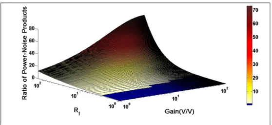
Figure 2.5 Preferred chopping technique (SCA or DCA) depending on the overall required gain and RF value. ...34
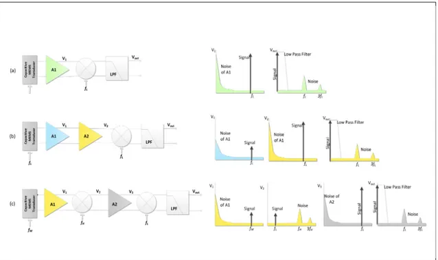
Figure 3.1 Connection of differential sensor capacitance to an interface circuit with parasitic capacitances. ...39 Figure 3.2 Diagram of the (a) single chopper amplifier, (b) two stage single
chopper amplifier, and (c) dual chopper amplifier with a capacitive transducer connected to the input. The frequency domain signal and noise representation for each system is also presented. ...41 Figure 3.3 Sensitivity factor of the chopper amplifier normalized by the
reference amplifier for a loading factor of 0.01. ...49 Figure 3.4 Sensitivity factor of the chopping amplifier normalized by the
reference amplifier for a loading factor of 1. ...49 Figure 3.5 Sensitivity factor of SCA for different total gains for sensor
capacitance of 100fF, 250fF, and 800fF. ...51 Figure 3.6 Normalized sensitivity factor of the TCA for different total gains and
sensor capacitances. ...56 Figure 3.7 Minimum Sensitivity factor in the TCA for (a) different total gains and
sensor capacitances and (b) ratio of first amplifier gain to total gain related to minimum sensitivity factor. ...57 Figure 3.8 Normalized sensitivity factor of the DCA for the gains of (a) 40 dB
and (b) 60 dB for sensor capacitance of 100 fF (red lines) and 500 fF (blue lines). ...59 Figure 3.9 (a) Normalized minimum sensitivity factor of the DCA for different total
gains, and (b) ratio of gain of the first amplifier to the total gain to reach the minimum sensitivity. ...61 Figure 3.10 (a) Normalized minimum sensitivity factor of DCA2 for different total
gain, (b) Ratio of the gain of first amplifier to the total gain to reach the minimum sensitivity. ...62 Figure 3.11 Ratio of minimum sensitivity factor in DCA to DCA2 ...63
Figure 3.12 (a) Preferred chopping technique between SCA, TCA and DCA2, and (b)
preferred chopping technique between SCA, TCA and DCA for
different total gain and sensor capacitance. ...65 Figure 3.13 Ratio of minimum sensitivity factor between (a) SCA/DCA2, (b)
Figure 3.14 Flow graph of the preferred chopping technique based on total gain
and sensor capacitance. ... 69
Figure 4.1 Diagram of (a) the modified DCA with an input capacitive MEMS transducer, and (b) the spectrum of signals and noise at key nodes of the circuit. ... 77
Figure 4.2 Diagram of (a) the noise voltage summation of the amplifiers in the dual path, and (b) the resulting equivalent summation of their noise current. ... 80
Figure 4.3 Different cascaded amplifier structures: (a) single-path, (b) single-path with doubled second stage gain, and (c) dual-path. ... 82
Figure 4.4 Schematic of the proposed circuit. The Rbias resistorsare implemented as pseudo-resistors to achieve high resistance values. ... 83
Figure 4.5 Schematic of the (a) controllable complementary-switch mixer, and (b) its control circuit. ... 84
Figure 4.6 Schematic of the first stage amplifier. ... 85
Figure 4.7 Schematic of the second stage amplifier. ... 88
Figure 4.8 Schematic of the adder with embedded gm-C filter. ... 89
Figure 4.9 Micrograph of die active area of 550 × 250 µm. ... 90
Figure 4.10 Output voltage the DCA in single path mode with ... 91
Figure 4.11 Input-referred noise voltage over frequency of the DCA in (a) single path mode, and (b) in dual path mode. ... 92
Figure 4.12 Integrated input-referred noise voltage of the DCA in single path mode and in dual path mode within 500 Hz integration ranges. ... 93
Figure 4.13 SNR (0.5 – 4 kHz) and THD of the DCA in single path mode and dual path modes for different input signal amplitudes. ... 95
Figure 5.1 Schematic of the proposed circuit ... 101
Figure 5.2 Frequency response of the circuit for different capacitor bank (C3) values. ... 104
Figure 5.3 Output spectrum for a 150 Hz input signal of -81 dBV ... 105
Figure 5.5 Noise contribution of the third amplifier and other circuits with
enabled and disabled third chopper. ...106 Figure 8.1 Proposed topology for the next generation of signal conditioning
LIST OF ABREVIATIONS ADC Analog to Digital Converter
BW Bandwidth CAGR Compound Annual Growth Rate
CIS Contact Image Sensor
CMOS Complementary Metal Oxide Semiconductor DCA Dual Chopper Amplifier
FM Frequency Modulation
FVC Frequency to Voltage Converter
LPF Low Pass filter
MEMS Micro Electro-Mechanical Systems PEF Power Efficiency Factor
PVT Process, Voltage and Temperature variations
PWM Pulse-Width Modulation
SAR Successive Approximation Register SCA Single Chopper Amplifier
SNR Signal to Noise Ratio
TCA Two-stage Chopper Amplifier
THD Total Harmonic Distortion VLSI Very Large-Scale Integration
LIST OF SYMBOLS AND UNITS Z Zepto f Femto n Nano m Mili µ Micro k Kilo M Mega V Volt W Watt Hz Hertz F Farad dB Decibel P Power I Current R Resistor C Capacitance T Temperature SF Sensitivity Factor gm Transconductance W Width of transistor L Length of transistor
Cox Oxide capacitance
Vn Thermal noise
Cgg Input capacitance of transistor
f Frequency
INTRODUCTION Background and motivation
Sensors are becoming more and more prevalent in a wide range of applications touching our daily lives. They are a crucial component in environment sensing (Maruyama, Taguchi, Yamanoue, & Iizuka, 2016; X. Wang et al., 2017), medical equipment (Lopez et al., 2018; Yazicioglu, Kim, Torfs, Kim, & Hoof, 2011), smart homes (Byun, Jeon, Noh, Kim, & Park, 2012; Vujović & Maksimović, 2015), automotive electronics (Altaf, Zhang, & Yoo, 2015; Cooley, Wallace, & Antohe, 2002; Hilt, Gupta, Bashir, & Peppas, 2003; Luo et al., 2008; Vasilyev, Rewienski, & White, 2006), and smart portable electronics (Charlot, Sun, Yamashita, Fujita, & Toshiyoshi, 2008; Rashidi & Mihailidis, 2013; Shi et al., 2009; Yazdi, Mason, Najafi, & Wise, 1996). For example, smartphones include sensors such as face ID, barometer, three-axis gyro, accelerometer, proximity sensor, ambient light sensor and modern cars easily contain more than 100 sensors used for several functions such as basic operation (engine temperature, oil pressure), information and driving help (parking aid, tire pressure measurement), comfort (air conditioning, defogging), safety (airbag deployment, yaw rate sensing) and optimization (exhaust gas monitoring), etc. (Wilcox & Howell, 2005; J. Zhao, Jia, Wang, & Li, 2007).
Among different kinds of sensors, MEMS (Micro-ElectroMechanical Systems) -based sensors are implemented broadly nowadays. They have the advantage of small size, low cost, low power consumption, and high reliability. This kind of sensor had a significant growth during the past years.
The growth of revenues from MEMS systems in different applications from 2014 to 2024 is shown in Figure 0.1. As displayed, consumer electronics, automotive, and medical sensors have larger growth. In 2024, MEMS market revenues will come mostly from consumer electronic applications, estimated to reach US$13B. Moreover, automotive applications are
estimated to reach US$6B, and medical sensors are estimated to reach US$5B worldwide (Yole, 2017).
To compare the growth of MEMS systems with other kinds of sensors, segmented revenues are shown from 2015 to 2021 in Figure 0.2. As shown, it is estimated that the market for MEMS and sensor devices will grow from US$49B in 2018 to US$66B in 2021. Such a figure is an impressive 12% compound annual growth rate (CAGR). Also, it is shown that the revenue of MEMS and contact image sensors (CIS) are remarkable in comparison with others. This revenue was US$10.5B for MEMS in 2015, and it is estimated to jump to US$21B in 2021. Moreover, new applications of MEMS sensors are also emerging with use in smart homes and buildings recently. The sensor market has a CAGR of 13.4% in smart homes and buildings from 2016 to 2022, and it is predicted to be US$1.7B U in 2022 (Muller, Gambini, & Rabaey, 2012).
MEMS sensors can respond to physical parameters such as radiation (Augustyniak et al., 2013; Buchner et al., 2007; Musca et al., 2005), pressure (Ge, Wang, Chen, & Rong, 2008; Mohan,
Figure 0.1 Revenues from the global micro-electromechanical systems (MEMS) market from 2014 to 2024, by application,
Malshe, Aravamudhan, & Bhansali, 2004; Palasagaram & Ramadoss, 2006; Y. Zhang, , movement (Fitzmaurice, 1993; B. Lee, Bang, Kim, & Kim, 2011; Mehra, Werkhoven, & Worring, 2006; Rohs et al., 2007), flow (Kao, Kumar, & Binder, 2007; E. Meng & Yu-Chong, 2003; Nguyen, Paprotny, Wright, & White, 2015; Shibata, Niimi, & Shikida, 2014; Y.-H. Wang, Lee, & Chiang, 2007), chemical (Holthoff, Heaps, & Pellegrino, 2010; Lavrik, Sepaniak, & Datskos, 2004; Saxena, Plum, Jessing, & Baker, 2006), or temperature (Khazaai, Haris, Qu, & Slicker, 2010; Que, Park, & Gianchandani, 1999; Sinclair, 2000).
Problems and challenges statement
The output of MEMS sensors usually are not proper for signal processing such as analog to digital conversion. Accordingly, signal conditioning circuits should be integrated at the outpout of the sensors before further signal processing. These circuits preserve the integrity of the sensor’s signal and properly amplify it while maintianing the signal to noise radio and minimizing distortion. Accordingly, signal conditioning circuits are implemented to amplify the signal with low added noise in order to make the signal ready to process in an analog or digital fashion. The frequency range of detected signals in MEMS-based sensors are up to a few kHz, and in biomedical applications it can be as small as a few Hz. For example, the
Figure 0.2 MEMs and sensors market anticipation, taken from (Yole, 2017)
frequency of brain waves can be small as 0.5 Hz and the amplitude can be as small as 5 µV. As a result, removing the flicker noise of the signal conditioning circuit is the most important challenge in these applications. In additon of the flicker noise, the thermal noise should be minimized to be able to detect the signal properly. Also, in capacitive sensors, the effect of input capacitance of signal the conditiong circuit should be considered, as it can negatively impact sensitivity. Accordingly, the signal conditioning circuit should be optimized for flicker and thermal noise, and for low input capacitance. At last, the power consumption should be minimized to be able to allow for the sensor to be deploed in battery-operated environments, where sensors are often needed. However, there is a tradeoff between decreasing the noise, power consumption, and input capacitance of the circuit, and this thesis aims at investigating this tradeoff and proposing signal conditioning circuit architectures that can provide a good tradeoff.
Signal conditioning circuit overview
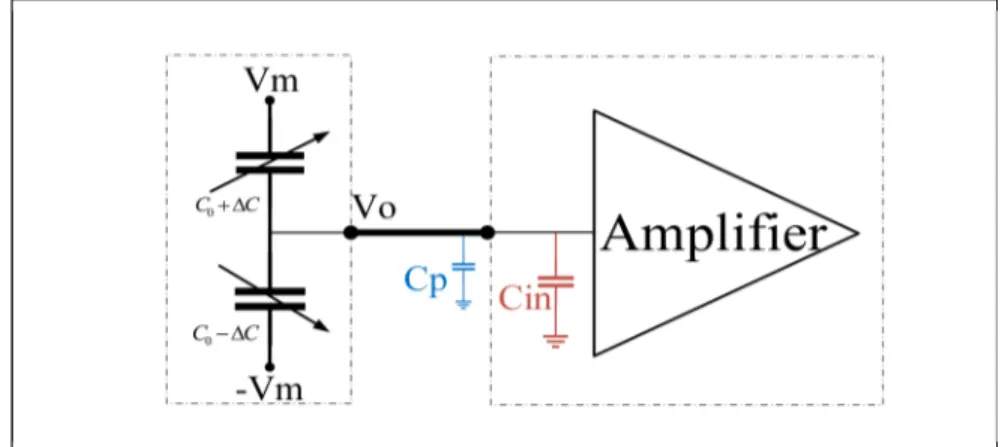
The schematic of a typical sensor is shown in Figure 0.3. As shown, it consists of two main parts: MEMS transducer and signal conditioning circuit. The physical parameters such as temperature, pressure, position, movement, and vibration are detected and converted to an electrical signal in a MEMS transducer and then transferred to a signal conditioning circuit for amplification and filtering. Since the output signal produced by a sensor is usually not suitable to directly process in the digital or analog domain, signal conditioning is a method of preparing an analog signal for further processing. The signal conditioning usually involves amplification and filtering. The goal of the filtering stage is eliminating the noise from the signal of interest and the aim of the amplifier is to increase the performance of the circuit. MEMS sensors have different electrical characteristics. The principle of operation of the sensor determines the nature of sensor output, which in turn determines the signal conditioning circuit requirement. Thus, depending on the sensor output, a circuit can be designed in different configurations to extract the sensor output (Master, 2010).
To detect the signal in the transducer, a capacitive bridge, or a resistive bridge could be implemented to convert the physical parameters to the electrical signal. The output of resistive sensors usually varies from few hundreds of µV to tens of mV, and the output of the capacitive sensor can be as small as femto farad. Usually capacitive sensors are preferred to resistive ones because of their high sensitivity, low power consumption, and high reliability. In the capacitive (resistive) sensing, there is a nominal value for the capacitance (resistance) and with a physical variation, the value of the capacitance (resistance) is changed. By measuring this variation, the amount of physical parameter change will be defined. Performance of the MEMS sensors is dependent to both the MEMS transducer design and the signal conditioning circuit design. In this work, design of the signal conditioning part will be investigated. This circuit should be precise enough to be able to integrate with different MEMS transducers.
A capacitive sensor and its integration with a signal conditioning circuit is shown in Figure 0.4. The output voltage of this transducer equals to:
m o V C C V 0 Δ = (0.1)
Where, C0 is the nominal capacitance sensor, Vm is the excitation voltage and ΔC is the
capacitance variation.
However, when this transducer is connected to a signal conditioning circuit, the input
capacitance of the signal conditioning circuit will be affected on the performance of the transducer. As a result, the output voltage of capacitive sensor equals to:
m in P o V C C C C V + + Δ = 0 2 2 (0.2)
where Cp is the parasitic capacitance of wiring, and Cin is the input capacitance of signal
conditioning circuit. With the proper integration of the MEMS transducer with signal conditioning circuit, the Cp could be removed, but the value of Cin is dependent on the signal
conditioning circuit design. For small sensor capacitances, the value of the input capacitance of a signal conditioning circuit is important, and it should be considered in the design of signal conditioning circuit. The voltage produced by the capacitive sensor is transferred to the signal conditioning circuit. Consequently, the value of this voltage should be larger than the input noise of signal conditioning circuit to be detectable. Thus, another important factor that should be considered in the design of a high sensitivity circuit is the input noise level of the signal conditioning circuit. It should be noticed that decreasing the noise level could be possible at the cost of increasing the input capacitance. As a result, the noise level of the signal conditioning circuit should be decreased while keeping the input capacitance low. Moreover,
Figure 0.4 Capacitive sensing and its integration with signal conditioning circuit
the power consumption and area are the two other factors that should be considered for sensors in portable devices.
To reach these characteristics, many different signal conditioning circuit architectures are possible. An appropriate choice of architecture is beneficial to detect the signal with enough sensitivity and gain and make it ready for processing.
Research goals and objectives
The goal of this research is to investigate novel signal conditioning circuits to enable the readout of several MEMS-based transducers. These circuits will have to feature low power consumption and noise reduction techniques, and also be agile (i.e., reconfigurable) to accommodate various capacitive and resistive MEMS transducer types.
The following research objectives were tackled during this Ph.D.:
• Design a best-fit signal conditioning circuit based on the sensor characteristics and required gain;
• Enable energy efficient operation by targeting ultra-low power consumption to enable the use of multiple sensors in portable devices with a longer battery life and better performance;
• Minimizing the noise in order to be able to detect the smallest variation in the sensors; • Minimizing the input capacitance in order to prevent the loading effect on the capacitive
sensors and maintain the sensitivity; and
• Improving the SNR of the signal conditioning circuit to maintain the input signal integrity;
Our Approach
In order to achieve the above-mentioned goals and objectives, various signal conditioning circuits are investigated and compared. For our desired application, a chopper technique is preferred to reach the small noise floor. Then, different chopping techniques, such as single
chopper amplifier (SCA), two-stage chopper amplifier (TCA), and dual chopper amplifier (DCA), are considered for capacitive and resistive sensors.
First, the power consumption, the input noise floor, and the sensitivity of different chopping techniques are analysed for different gains and sensor capacitances. Then, a methodology is proposed to choose the proper chopping technique and design a circuit to reach the highest sensitivity or the desired sensitivity with minimum power consumption in each gain and sensor capacitance. It is shown that the input capacitance of the signal conditioning circuit is important to achieve the best capacitance sensitivity, and this factor is considered in the analysis of the sensitivity of different chopping techniques for the first time. It is shown that the minimum sensitivity factor is achievable by the DCA structure. The DCA has the freedom of distribution of gain between the two stages. As a result, based on the value of sensor capacitance, DCA can be designed in a way that minimizes both the input noise floor and the input capacitance.
Based on the methodology, a novel circuit is designed to improve the sensitivity performance and minimize the power consumption in the signal conditioning circuit. In this design, a dual-path dual-chopper amplifier with two different supply voltages is proposed and fabricated in the GlobalFoundries 0.13µm CMOS technology. A low-noise low-supply voltage amplifier is implemented at the first stage. In this amplifier, high current and low supply voltage are implemented to minimize the power consumption and the noise at the same time. Then, the second stage includes two paths of two high gain amplifiers and each of them is chopped separately. Enabling of one path or two paths together is possible in this design to reach configurable gain. It is shown that utilising the dual paths helps to reach a higher gain and a higher SNR. A four-input gm-C filter is utilized to add the signals from the two paths, which
helps to reduce the switch-nonidealities which are produced in the two paths too.
In the last design, a signal conditioning circuit with the three stages and the triple-chopping is designed and simulated in the same 0.13 µm CMOS technology. The first stage is used to reach the low noise and low-input capacitance amplifier. The amplifier of this stage has a high current and low supply voltage to reach the low noise floor and the low power consumption. The
second and third stages are a resistive feedback amplifier and a capacitive feedback amplifier to attain low noise low pass filtering with a tunable bandwidth. The miller effect in the capacitive feedback amplifier helps to reach a bandwidth as small as 1 Hz without the need of a very large capacitance. A small bandwidth contributes to a lower integrated input noise and improves SNR. Since three blocks are chopped, there is no significant flicker noise in this circuit. The corner frequency of this circuit is 0.5 µHz and allows for near-DC high precision operation.
Main Contributions and Novelties of the Thesis
To the best of the author’s knowledge, the first signal conditioning circuit which considers the effect of input capacitance on the methodology design is presented in this research work. Based on the above objectives and methodologies, the main contributions of this work are:
• Proposing a methodology to design an optimized signal conditioning circuit with a chopping technique based on the sensor capacitance and the required total gain. This methodology helps to design a circuit to reach the maximum possible sensitivity, or reach the desired sensitivity with the minimum power consumption.
• Design and fabrication of dual path-dual chopper amplifier. A low-noise and ultra-low power circuit is achieved. The power efficiency factor (PEF) of this circuit is 11 for the single-path circuit and 13 for the dual-path circuit, which indicates a good trade-off of noise and power consumption. The small power consumption of this circuit is 2.66 µW from the 0.7 V supply and 3.26 µW from the 1.2 V supply voltage. The noise floor achieved is of 25 nV/√Hz.
• Design and simulation of a low-power low-noise signal conditioning circuit with sub-µHz noise corner frequency and tunable bandwidth. This circuit has a low noise and a low power consumption. Simulation results show that with this circuit, a corner frequency of 0.5 µHz with a noise floor of 20.5 nV/√Hz is achievable. This structure helps to measure the signal around DC frequency. In addition, the bandwidth is tunable, and it can be set based on the application. A bandwidth as small as 1 Hz is achievable in this circuit, which helps to reduce the integrated input noise and improve the SNR. The power efficiency factor of 4 and SNR of 115.7 dB for the bandwidth of 100 Hz is achievable with this circuit.
Thesis Organization
The thesis has been divided into 6 chapters. The first chapter summarizes the literature review and the recent implemented architectures for relevant signal conditioning circuits. The most common implemented signal conditioning circuits are categorized, and their advantages and disadvantages, as well as common features, are be discussed.
Chapter 2 explains the important factors in the design of a signal conditioning circuit for MEMS. An overview of chopping technique is explained. A brief discussion of the papers that compose this thesis is done in this chapter, and their relevance to the Ph.D. work is described.
Chapter 3 is a methodology paper. In this paper, which was published in the Journal of Low Power Electronics and Applications in 2017, three different chopping techniques are considered, and their sensitivity and power consumption are extracted based on the required gain and sensor capacitance. Moreover, the proper chopping technique and the way of designing a chopping circuit to reach the optimum performance in each gain and sensor capacitance is shown in this paper.
In chapter 4, a dual-path dual-chopper amplifier with two supply voltages is designed and fabricated in the GlobalFoundries 0.13µm CMOS technology. This chapter is a paper that was published in IEEE Transactions on Circuits and Systems I: Regular Papers in 2019.
In chapter 5, a low-noise low-power signal conditioning circuit with configurable bandwidth and sub-µHz noise corner frequency for use in resistive and capacitive MEMS sensors that requires minimal capacitive loading is designed and simulated. This chapter is a paper that was submitted to IEEE Sensors Letters in 2019.
Finally, the overall results and the contributions are discussed in chapter 6. The conclusion and suggestions for future work are presented at the end of the thesis.
LITERATURE SURVEY 1.1 Different electrical readout techniques
One of the most important parts of any sensor is a readout system capable of monitoring physical changes and converting them to an electrical signal. In this section, we discuss the details of sensor readout techniques that can be classified broadly as capacitive sensing and resistive sensing.
1.1.1 Capacitive sensing
Capacitive sensing is the dominant sensing mechanism in micro-electro-mechanical systems (MEMS) inertial sensors, since it has the advantages of low temperature coefficients, low power consumption, low noise, low cost and the potential of compatibility with integrated circuit (IC) fabrication technology. A simple configuration of capacitance is defined as shown in equation (1.1):
(1.1)
Where ɛr is the permittivity of the dielectric, ɛ0 is the permittivity of vacuum, A is the
overlapping area, and g is the distance. Capacitive sensors are designed to detect a signal based on changing the size of a gap (Baxter, 1997), overlap area (Baxter, 1997), or dielectric properties (Heidari, 2010).
In capacitive sensors based on changing the gap distance, the position is encoded as capacitance between two or more separate electrodes in the sense element. These capacitive sensors can be configured in different ways. One is a single variable capacitor where the
g A
capacitive sensors are designed such that they have two fixed plates and one movable plate in the middle. With an external acceleration the movable plate is displaced from its nominal position. The physical sizes of the gaps between the plates are changed and contributes to two different values of capacitance. The principal design objective of this capacitive sensor is to efficiently convert mechanical displacements and hence capacitive changes into an electrical signal. The other configuration is a capacitive half bridge where one capacitor with a positive positional dependency and other with negative positional dependency are connected at a common mode. Typically the change in capacitance is first converted to a voltage and then it can be further processed with various signal-conditioning blocks or an analog to digital converters (ADC). Capacitive sensing is widely used in pressure sensors, liquid-level gauges, accelerometers and humidity sensors, and proximity and position sensors (1998; Lazarus, Bedair, Lo, & Fedder, 2010; H. Lee, Chang, & Yoon, 2009; Lin et al., 2008; Yazdi, Ayazi, & Najafi, 1998; Y. Zhang, Howver, Gogoi, & Yazdi, 2011).
1.1.2 Piezoresistive sensing
In piezoresistive sensors, the resistivity is changed by the application of a physical stimulus, and the resulting resistance variation is measured to detect the value of physical stimulus. The change in resistance equals to:
t t l l
σ
π
σ
π
+ = Δ R R (1.2)where R is the initial resistance, ∆R is the change in resistance, πl and πt are the longitudinal
and transverse piezoresistive coefficients, respectively, and σl and σt are the lateral and
transverse stresses, respectively. The resistance can change in response to stimulus in two different categories: changes to the geometry or changes to the conductive properties of the resistor. Typically, a Wheatstone bridge circuit is implemented in resistive sensing as shown in Figure 1.1.
The output voltage is directly related to the change in the resistance with respect to the initial resistance R. The resistance change in the Wheatstone bridge is measured by the excitation voltage or current, and high excitation voltage or current is necessary for high bridge sensitivity, which results in high power consumption (Thanachayanont & Sangtong, 2007).
Piezoresitive sensors have a simple structure. They are tolerant to high shock conditions. They have low measurement uncertainty, and low nonlinearity and hysteresis error. However, they have more power consumption compared to capacitive sensors and they are more sensitive to temperature variations.
1.1.3 Comparison between methods by principle of output measurement
The advantages and disadvantages of capacitive and resistive sensors are shown in Table 1.1. Between the above-mentioned methods, capacitive sensing is preferred since it has the advantages of low temperature coefficients, low power dissipation, low noise, low-cost fabrication, and compatibility with VLSI technology scaling.
Figure 1.1 Wheatstone circuit taken from (Mutyala, Bandhanadham, Pan, Pendyala, & Ji, 2009)
Table 1.1 Comparison of different readout techniques Advantages Disadvantages Capacitive sensing • High sensitivity • Low temperature dependence • Capable of measuring very low frequency signals
• Low power circuit interface
• High temperature range • Compatibility with
VLSI technology
• Low frequency range • More complex interface
circuit
Resistive sensing
• Simple interface • High shock tolerance • Medium frequency range • Low sensitivity • Higher power consumption • Temperature dependence •
1.2 Literature survey of signal conditioning circuits
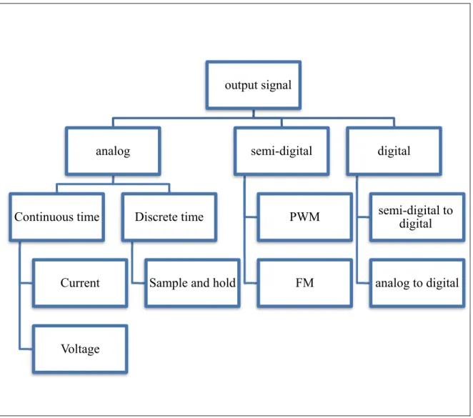
After detecting a signal in a sensor, the signal should be amplified in a signal conditioning circuit. Figure 1.3 shows the classification of signal conditioning circuits based on their outputs. As shown in this figure, output can be analog, semi-digital, and digital. Analog output can be achieved by discrete time or continuous time architectures. In a discrete time architecture, switched capacitor amplifiers are usually implemented. For continuous time amplification, an input stimulus is converted to a voltage or current and then amplified. Architecture such as chopping can be utilized in continuous time amplification to improve the performance of the circuit. Another category of amplification of the signal is based on the architecture that produces a semi-digital output. This category includes pulse-width
modulation and frequency modulation. To produce a digital signal at the output, an analog signal can be converted to digital signal using an analog to digital converter or digitalizing a semi-digital signal.
In the design of a signal conditioning circuit, power, noise, and sensitivity are the three most important challenges that should be considered. Regarding the application, the output signal can be digital, analog or semi-digital. In the following, the methods to produce these kinds of outputs are briefly described, and at the end, the advantages and disadvantages of each will be explained. output signal analog Continuous time Current Voltage Discrete time
Sample and hold
semi-digital PWM FM digital semi-digital to digital analog to digital
1.2.1 Techniques to produce an analog output signal
An analog output signal from a signal conditioning circuit can be obtained by either continuous time or discrete time methods. Switched capacitor circuits are used in discrete time methods to amplify the detected signal. In the continuous time architecture, a detected signal is amplified in either voltage or current mode. Because of the low frequency range of the input signal, chopper modulation is often implemented in continuous time methods. Some of the state-of-the-art design of signal conditioning circuits with analog outputs are described in the following sections.
1.2.1.1 Discrete time signal conditioning circuit
A switched capacitor circuit can be implemented in a signal conditioning circuit to move the charge in the sensor to the output. In the switched capacitor circuit, the sensing and reference capacitors are charged with opposite polarity voltages, which causes charge to propagate due to the voltage created by the difference of the capacitances to the output. A model of switched capacitor circuit is shown in Figure 1.3.
int
C C V
Vout = P Δ (1.3)
Where ΔC is the capacitance difference between Cs and Cr are the sensing capacitance and
reference capacitance, respectively, Vp is the excitation voltage, and Cint is the capacitance of
the feedback capacitor.
The switched capacitor circuit provides a virtual ground and robust dc biasing at the sensing nodes. As a result, the sensing node is insensitive to parasitic capacitances and undesirable changes (Reddy, 2011). Moreover, the switched capacitor circuit is insensitive to the temperature (Aezinia, 2014). This architecture is implemented in works such as (Chavan & Wise, 2000; Kajita, Un-Ku, & Temes, 2002; Kulah, Junseok, Yazdi, & Najafi, 2003; M. Lemkin & Boser, 1999; M. A. Lemkin, 1997; Lu, Lemkin, & Boser, 1995; Ogawa, Oisugi, Mochizuki, & Watanabe, 2001; Ranganathan, Inerfield, Roy, & Garverick, 2000; Smith, Nys, Chevroulet, DeCoulon, & Degrauwe, 1994). The main disadvantages of a switched capacitor is a high noise floor, which is caused by high kT/C noise at low capacitance, high thermal noise if resistive MOS switches are implemented, and noise folding (Jiangfeng, Fedder, & Carley, 2004). In addition, they need a precise design of non-overlapping clock (Aezinia, 2014).
To reduce the kT/C in switched capacitor circuit, correlated double sampling (CDS) is utilized (Du et al., 2015; Du et al., 2017; Ranganathan et al., 2000) . Although CDS reduces the kT/C noise, noise folding and the thermal noise of resistive MOS switches still exist. In conclusion, the discrete time method is not preferred for high resolution signal conditioning due to its noise performance being worse than other methods.
1.2.1.2 Continuous time signal conditioning circuit
In continuous time sensing, there are two ways to measure the signal at the output: continuous time voltage sensing and continuous time current sensing. In voltage sensing, the physical
sensed signal is converted to a voltage and then amplified, while in the current sensing mode, the physical sensed signal is converted to a current and then amplified.
At low frequencies, flicker and offset are the dominant sources of noise in CMOS technology, and to achieve high sensitivity, it is important to remove them properly. Two methods are implemented in continuous voltage sensing to remove the flicker noise: auto zeroing and chopping. In auto zeroing, flicker noise is removed but the noise floor is increased because of noise folding (Enz & Temes; Rong Wu, Huijsing, & Makinwa, 2013). As a result, chopping is generally preferred in low-noise continuous time voltage sensing. The architectures of circuits using current sensing and voltage sensing are explained in the following sections.
1.2.1.2.1 Continuous time current-mode signal conditioning circuit
A current-mode signal conditioning circuit converts the capacitance difference to a current (Singh, Saether, & Ytterdal, 2009). A block diagram of a capacitance-to-current signal conditioning circuit is shown in Figure 1.4. In this figure, Cm and Cr represent the sensor
capacitance and fixed capacitance, respectively. Both of these capacitances have the same nominal value. At zero, the charging current (Ib) splits equally between these two capacitances,
Figure 1.4 Block diagram of a capacitance-to-current signal conditioning circuit taken from (Singh, Saether, & Ytterdal, 2009)
but with changes in the value of Cm the distribution of current between the two paths is altered.
The current is converted to a voltage by a resistive feedback amplifier. The output voltage of this amplifier is proportional to
Where Rf is the resistive feedback, C is the nominal capacitance, and ΔC is the difference
between the sensor capacitance (Cm) and reference capacitance (Cr).
The advantages of current mode sensing is that adding signals as currents is simple. A current-mirror-like scheme can be applied for improving the sensitivity while also simplifying the circuit (Haider et al., 2008). However, the disadvantage of this scheme is that nonlinearity can be produced by current leakage from the switches. Moreover, the parasitic capacitance at the common node electrode should be significantly smaller than the sensing capacitance to prevent degrading the performance (Banitorfian & Soin, 2011; Marcellis, Carlo, Ferri, & Stornelli, 2009; Pennisi, 2005; Scotti, Pennisi, Monsurrò, & Trifiletti, 2014; Singh et al., 2009).
1.2.1.2.2 Continuous time voltage-mode signal conditioning circuit with chopper stabilized amplifier
A chopper-stabilized amplifier is generally preferred in continuous time voltage-mode signal conditioning method. In a chopper stabilized amplifier, the desired signal is modulated to a higher frequency, amplified, and then demodulated (Bakker, Thiele, & Huijsing, 2000; Enz & Temes, 1996; Enz, Vittoz, & Krummenacher, 1987). In this fashion, the DC offset and flicker noise are decreased significantly (Enz et al., 1987). Figure 1.5 shows the chopping amplifier with its ideal waveform. To remove the flicker noise effectively, the chopper frequency should be larger than the flicker noise corner frequency.
C C C I R i R i R V V Vout op om f f f b Δ + Δ = = = − = 2 . . (1.4)
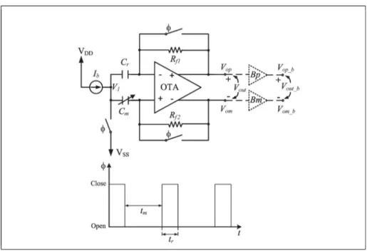
Although the chopping amplifier suppresses flicker noise, it is not an energy efficient technique. In (Fang, Qu, & Xie, 2006; Qu, Fang, & Xie, 2008; H. Sun et al., 2011), dual chopper amplifier (DCA) is implemented. In (H. Sun et al., 2011), a dual chopper amplifier design is proposed to minimize the power consumption and noise by chopping the sensed signals at two different clock speeds, the design of which is shown in Figure 1.6. The first clock is at a high frequency to remove the flicker noise while the second clock is at a significantly lower frequency to keep the unity gain bandwidth low. The optimized gain of the first amplifier to reach the minimum power consumption is given in Equation 1.5:
(
)
(
W L)
G C f L W C f G L L H H H H L L opt H . / / 3 2 1 2 1 = − (1.5) Figure 1.5 Chopping principle, taken from (Rong Wu,Where fL and fH are the second chopping frequency and first chopping frequency, respectively, CL and CH are the load capacitances of the second amplifier and first amplifier, respectively, WL/LL is the ratio of the width to length at the input to the transistor of the second amplifier, WH/LH is the same ratio but in the first amplifier, and G represents the total gain of the circuit.
In the equation (1.5) it is assumed that the noise from the first amplifier is dominant over the noise from the second amplifier, and so the noise produced by the second amplifier is not considered in that formula. This circuit is optimized for the parasitic capacitances, while the effect of the capacitance of the input transistor is not considered in the optimization. The effect of this transistor will degrade the performance of the sensor capacitance while the sensing capacitance is small.
As explained above, in a DCA two different frequencies are implemented to chop at two stages. Thus, there is a freedom of distribution of gain between the two stages that contributes to a reduced power consumption compared to a single chopper amplifier design. The drawbacks of this chopping technique is that clock non-idealities, such as charge injection and residual offset,
can degrade the performance. To remove clock non-idealities and improve the performance, a careful design of the clock is essential. Implementing properly designed switches, such as dummy or complementary switches, will improve the performance. Moreover, this chopping technique can be combined with other techniques such as the capacitively coupled technique (Denison et al., 2007; Fan, Huijsing, & Makinwa, 2012; Fan, Sebastianen, Huijsing, & Makinwa, 2010; Fan, Sebastiano, Huijsing, & Makinwa, 2011; P. Sun, Zhao, Wu, & Fan, 2012; R. Wu, Makinwa, & Huijsing, 2009), a ripple reduction loop (Kusuda, 2009, 2010; P. Sun, Zhao, Wu, & Fan, 2012; Yazicioglu, Merken, Puers, & Hoof, 2008), correlated double sampling (Belloni, Bonizzoni, Fornasari, & Maloberti, 2010; Belloni, Bonizzoni, Maloberti, & Fornasari, 2010; Enz & Temes, 1996; Shiah & Mirabbasi, 2014), the auto-zeroing technique (Witte, Makinwa, & Huijsing, 2007), and the multi-path chopping technique (Fan, Huijsing, & Makinwa, 2013; Fan, Huijsing, & Makinwa, 2012).
As a result, the combination of a DCA with other techniques could be an effective way to reach a low-power, high-sensitivity signal conditioning circuit.
1.2.2 Semi-digital signal conditioning circuit
A semi-digital output can be achieved with pulse-width modulation (PWM) or frequency modulation (FM). The principle of these two conditioning architectures are described in the following sections.
1.2.2.1 Frequency modulation based signal conditioning circuit
Capacitance-to-frequency converters have simple and straightforward structures. They usually use relaxation oscillators (Coskun et al., 2013; J. Zhang, Zhou, & Mason, 2007) or ring oscillators (Kyriakis-Bitzaros, Stathopoulos, Pavlos, Goustouridis, & Chatzandroulis, 2011; J. Zhang et al., 2007) to convert the capacitance to the frequency. Moreover, crossed-coupled oscillators (M. Shamsul Arefin et al., 2014; M. S. Arefin, Redouté, & Yuce, 2016b; Hua, Yan, Hassibi, Scherer, & Hajimiri, 2009; Wang, Weng, & Hajimiri, 2013) can be implemented to provide highly stable and lower phase-noise output frequencies for specific applications.
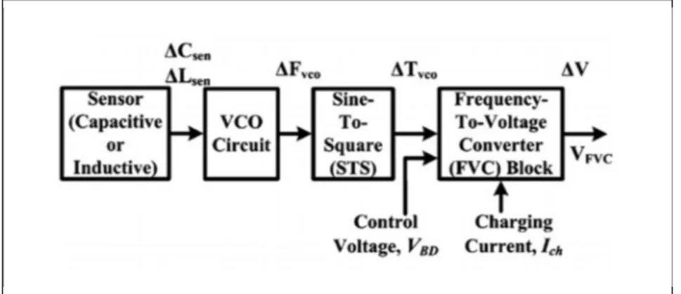
A block diagram of a capacitance-to-voltage circuit with frequency modulation (FM) is shown in Figure 1.7. A voltage-controlled oscillator (VCO) is implemented to convert the capacitance or inductive variation to the frequency. A sine-to-square circuit (STS) is implemented to convert the frequency variation to a time variation, and a frequency-to-voltage converter (FVC) circuit is used to convert the ΔTVCO to the voltage changes. The FVC is implemented to convert
an oscillation into a measurable voltage (M. Shamsul Arefin et al., 2014). The two main approaches for the implementation of FVC blocks are counter-based circuits (Hou, 2004; Kyriakis-Bitzaros et al., 2011) and integrator-based circuits (Bui & Savaria, 2008; Djemouai, Sawan, & Slamani, 2001).
The benefits of using frequency-based modulation are reduced phase, flicker, and white noises at higher frequencies (Ko, Tseng, & Lu, 2006; Mohammadi, Yuce, & Moheimani, 2012; Wang et al., 2013). However, FM circuits consume more power than current-to-voltage converter circuits (Bui & Savaria, 2008; Djemouai et al., 2001). Moreover, non-idealities such as parasitic capacitances, and feedback through air and track paths result in undesirable oscillations and degrade the performance of the overall circuit (Awad, 1988; Tyagi & Sumathi, 2017; Yili, Song, Nakayama, & Watanabe, 2000).
Figure 1.7 Block diagram of capacitive (or inductive) sensor to voltage with FM circuit taken from (M. S. Arefin,
1.2.2.2 Pulse-width modulation based signal conditioning circuit
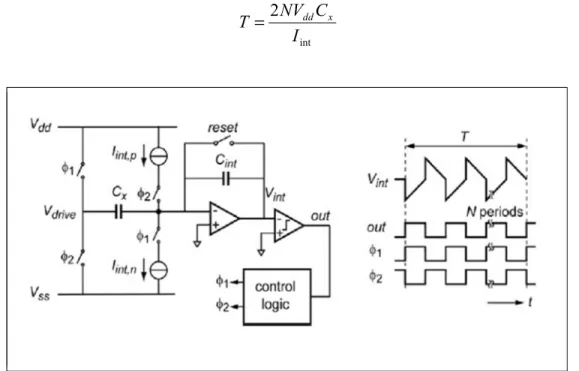
Pulse-width modulation (PWM)–based capacitive sensors are based on relaxation oscillators whose output period is proportional to the variation of the sensor capacitance. The operating principle of PWM circuits is reported in (Heidary & Meijer, 2008; Heidary, Shalmany, & Meijer, 2010; Tan, Shalmany, Meijer, & Pertijs, 2012), and Figure 1.8 shows a diagram of a signal conditioning circuit that converts capacitance to a pulse-width signal. In this structure, two phases are implemented. At phase Ø1, Vdrive is connected to a supply voltage, and the output
of the integrator steps down because of the amount of charge VintCx is transferred to Cint, and
then rises smoothly since a sinking current Iint,n discharges from Cint. To detect the moment
that Vint returns to its initial value, a comparator is used. At that moment, the phase triggers to
the phase Ø2. During Ø2, Vdrive is pulled to Vss and a sourcing currentIint,p charges Cint as in the
previous phase, but with an opposite polarity. This process will repeat N times, and the time period of this process is (Y. He, 2014) given by
int 2 I C NV T = dd x (1.6)
Figure 1.8 Typical ring oscillator for the measurement of a capacitive sensing element in pulse-width modulation, taken
Where T is the clock cycle, Vdd is the supply voltage, and Cx is the sensor capacitance. By
counting the clock cycles the sensor capacitance of Cx will be defined.
Pulse-width modulation can be designed to have relatively high resolution and handle a very large input capacitance range (Heidary & Meijer, 2008; Meijer & Iordanov, 2001). Interfaces that are based on relaxation oscillators are operated asynchronously and thus do not require a clock signal. Period-modulation-based capacitive sensor interfaces can be quite flexible, and, by using a sample digital divider, they can be simply converted to measurement time by counting the duration of multiple output periods (Heidary et al., 2010; Xiujun & Meijer, 2002). However, the power consumption is high in this implementation and are therefore not suitable for use in energy-constrained applications (Pertijs & Tan, 2013). To reduce the power consumption, the pulse-widthmodulation is combined with other techniques such as negative-feedback loops (Heidary & Meijer, 2008; Meijer & Iordanov, 2001), piece-wise charge transfer techniques (Y. He, Chang, Pakula, Shalmany, & Pertijs, 2015), and chopping and three-signal auto-calibration techniques (Tan et al., 2012). The output of PWM is strongly dependent on MOSFET transconductance, parasitic capacitance, and resistance values (M. S. Arefin, Redouté, & Yuce, 2016a; Bruschi, Nizza, & Piotto, 2007).
1.2.3 Digital output
To produce a digital output, analog-to-digital converters (ADCs) can be implemented to convert the voltage to a digital signal. These ADCs include successive approximation register (SAR) analog-to-digital converters (Brenk et al., 2011; Hsieh & Hsieh, 2018; Hwang, Park, Song, & Jeong, 2018; Mao, Li, Heng, & Lian, 2018; Sadollahi, Hamashita, Sobue, & Temes, 2018; D. Zhang, Bhide, & Alvandpour, 2012; Zou, Xu, Yao, & Lian, 2009) and ΔΣ modulators (Jung, Duan, & Roh, 2017; Park, Cho, Na, & Yoon, 2018; Rout & Serdijn, 2018; Sanyal & Sun, 2017). Successive approximation register (SAR) ADCs have low power consumption and moderate resolution (Hariprasath, Guerber, Lee, & Moon, 2010; Liu, Roermund, & Harpe, 2017; Tai, Hu, Chen, & Chen, 2014). ΔΣ modulators are suitable for high resolution applications, but have low energy efficiency (Paavola et al., 2007; Shin, Lee, & Kim, 2011;
Tan et al., 2013). Semi-digital-to-digital converters include frequency-to-digital convertors (Brookhuis, Lammerink, & Wiegerink, 2015; Cardes et al., 2018; Chiu, Hong, & Wu, 2013; Elhadidy, Shakib, Krenek, Palermo, & Entesari, 2015) and time-to-digital convertors (Danneels, Coddens, & Gielen, 2011; S. Lee et al., 2007). Time-to-digital convertors have a simple structure (e.g., counters), but usually they do not have a high resolution as their iterative discharging process requires 2N cycles for N-bit resolution (Sanyal & Sun, 2017). The
frequency-to-voltage convertors that VCO has implemented suffer from non-linearity problems and have a high sensitivity to process, voltage, and temperature (PVT) variations (Sanyal, Li, & Sun, 2018). Digital output can also be achieved by using the combination of frequency-to-voltage converters and ADCs (Elhadidy, Elkholy, Helmy, Palermo, & Entesari, 2013; Gaggatur, Dixena, & Banerjee, 2016; Helmy et al., 2012; Matsumoto & Esashi, 1993).
1.2.4 Comparison of different application areas
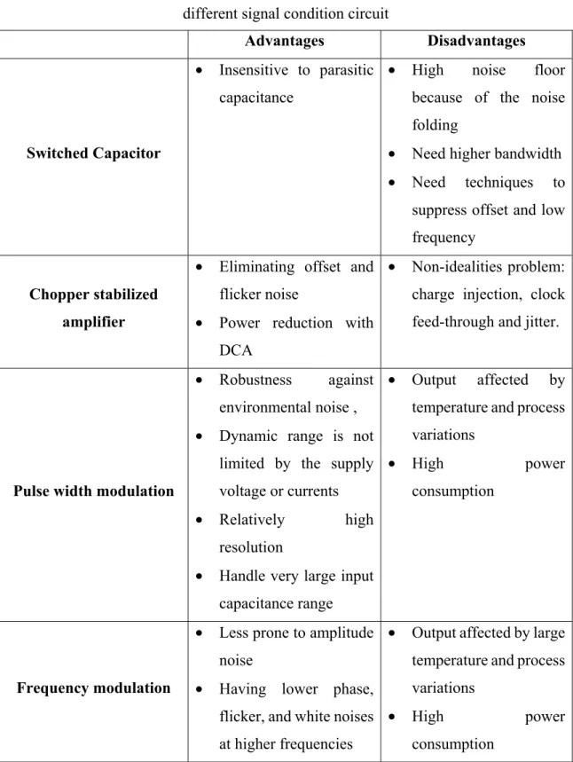
In this section, a review of different application areas and the requirements of sensor circuits implemented in those areas is given. As discussed previously, MEMS applications work in a low frequency range of up to a few kHz, and circuits applied here also need to have high resolution and a low-power signal conditioning circuit is necessary to detect small variations in the sensors. Each architecture for signal conditioning circuits has its benefits and limitations, and the most important of these are shown in Table 1.2. Among these architectures, the chopping technique is a well-suited option for low noise and low frequency applications.
Moreover, the power consumption of the chopping technique could be decreased significantly with the proper design of a dual chopper amplifier. The limitation of the chopper technique is that it is sensitive to clock non-idealities, and the input capacitance of the circuit can degrade the sensitivity performance. With a combination of the dual chopper technique with other techniques such as a ripple reduction loop, multi-path circuits, switch non-idealities can be decreased. Furthermore, the dual chopper amplifier gives us the freedom to design a circuit with a minimum input capacitance that also contributes to maximize the sensitivity during capacitive sensing.
Table 1.2 Summary of advantages and disadvantages of different signal condition circuit
Advantages Disadvantages
Switched Capacitor
• Insensitive to parasitic capacitance
• High noise floor because of the noise folding
• Need higher bandwidth • Need techniques to
suppress offset and low frequency
Chopper stabilized amplifier
• Eliminating offset and flicker noise
• Power reduction with DCA
• Non-idealities problem: charge injection, clock feed-through and jitter.
Pulse width modulation
• Robustness against environmental noise ,
• Dynamic range is not limited by the supply voltage or currents
• Relatively high resolution
• Handle very large input capacitance range
• Output affected by temperature and process variations
• High power consumption
Frequency modulation
• Less prone to amplitude noise
• Having lower phase, flicker, and white noises at higher frequencies
• Output affected by large temperature and process variations
• High power consumption
DESIGN CONSIDERATIONS OF SIGNAL CONDITIONING CIRCUITS FOR CAPACITIVE AND RESISTIVE SENSORS
The goal of this work is designing a signal conditioning circuit to be applicable for MEMS sensors. This circuit should be able to read signals from both capacitive and resistive sensors. At the MEMS transducer, a physical stimulus is converted to an electrical signal, and the electrical signal is amplified in the signal conditioning circuit. To have a proper MEMS sensor, the transducer, signal conditioning circuit, and their integration should work well to have a high performance circuit. The design of the MEMS transducer is not the scope of this work. However, by considering the characteristics of the MEMS transducer, the signal conditioning circuit is designed to maximize the performance.
The detected signal from the MEMS transducer could be as small as atto Farads in the capacitive sensor, and as small as micro volts in the resistive sensor for a frequency range of up to a few kHz. As a result, the signal conditioning circuit must have the capability of reading a low-amplitude low-frequency signal, and then amplify it properly to be suited to more processing. As a result, the input noise of the signal conditioning circuit should be smaller than the detected signal by the MEMS transducer. On the other hand, when a signal conditioning circuit is added to the capacitive sensor, it adds some parasitic capacitance to the transducer, and, based on the value of sensor capacitance, this parasitic could degrade the performance. The smaller sensor capacitance, the more important the input capacitance of signal conditioning circuit is.
In other words, the signal could not be readable even with a very low noise signal conditioning circuit that has a large input capacitance. As a result, both the input noise and the input capacitance should be minimized. As the frequency range of signal conditioning circuit is from DC to few kHz, the dominant noise is the flicker noise. The formula of flicker noise for a CMOS transistor equals to:
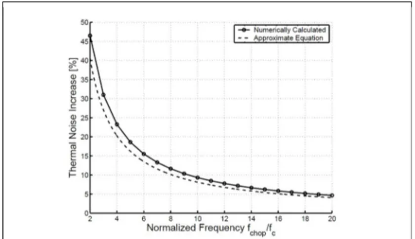
In the oxide capacitance, W and L are the width and the length of the transistor, respectively and kf is the flicker noise coefficient. With increasing dimension of the transistor, flicker noise is decreased. However, to have a low input noise in low frequencies, a technique should be implemented to suppress the flicker noise completely. Among the different techniques to remove the flicker noise, the chopping technique is preferable. In this technique, the signal is modulated to the higher frequency, amplified and then demodulated to the baseband as shown in Figure 2.2. As a result, flicker noise can be suppressed completely.
There are many constraints that should be considered in the design of a chopper amplifier. The most important of them is choosing the proper chopper frequency. To prevent the flicker noise down-folding, the chopping frequency should be larger than the corner frequency (Nielsen, 2004). Figure 2.3 shows the percentage of increasing noise floor regarding the ratio of chopping frequency to corner frequency. As shown, the chopping frequency should be at least ten times larger than the corner frequency to have less than a 10% increase in the noise floor. On the other hand, the chopping frequency should be in the bandwidth range not to degrade the signal amplitude. As a result, larger chopping frequency demands larger bandwidth that contributes to more power consumption.
WLf C k V ox f f = (2.1)
In addition of flicker noise, a careful design should be done to minimize the thermal noise. The thermal noise of a CMOS transistor equals to:
where k is Boltzmann’s constant, T is the absolute temperature, and gm is the transconductance,
which can have a value that is different in the subthreshold and saturation region. At the saturation region, to reduce the thermal noise, transconductance of transistor should be increased which means more current and larger ratio of W/L. However, a larger ratio of W/L contributes to a larger dimension for the transistor and will increase the input capacitance. Because of the limitation in power consumption and input capacitance of a single-chopper amplifier, a dual-chopper amplifier is proposed as shown in Figure 2.4. As shown in this architecture, two different chopping frequencies are implemented to chop two amplifiers. In the dual-chopper amplifier, the signal is chopped with a high frequency modulator, then amplified, and subsequently, it will be chopped with another chopping frequency to send it to the lower frequency, and then will be amplified again at the second amplifier. At last, it is demodulated to the baseband. This structure gives a greater degree of freedom, and with the
m n
g kT
V = 4 (2.2)
Figure 2.2 Thermal noise increase based on normalized frequency fchop/fc, taken from