HAL Id: hal-01007403
https://hal.archives-ouvertes.fr/hal-01007403
Submitted on 7 Jul 2018
HAL is a multi-disciplinary open access
archive for the deposit and dissemination of
sci-entific research documents, whether they are
pub-lished or not. The documents may come from
teaching and research institutions in France or
abroad, or from public or private research centers.
L’archive ouverte pluridisciplinaire HAL, est
destinée au dépôt et à la diffusion de documents
scientifiques de niveau recherche, publiés ou non,
émanant des établissements d’enseignement et de
recherche français ou étrangers, des laboratoires
publics ou privés.
Ultra-wideband GCPW-MS transitions for
characterising microwave and photonic components
based on thin polymer
Mohammed El Gibari, Dominique Averty, Cyril Lupi, Hongwu Li, Serge
Toutain
To cite this version:
Mohammed El Gibari, Dominique Averty, Cyril Lupi, Hongwu Li, Serge Toutain. Ultra-wideband
GCPW-MS transitions for characterising microwave and photonic components based on thin polymer.
Electronics Letters, IET, 2011, 47 (9), pp.553-555. �10.1049/el.2010.3745�. �hal-01007403�
Ultra-wideband GCPW-MS transitions for
characterising microwave and photonic
components based on thin polymer
M. El-Gibari, D. Averty, C. Lupi, H. Li and S. Toutain
Back-to-back grounded coplanar-microstrip transitions with an unpat-terned bottom ground plane and without via-holes are analysed. Theoretical results are compared to experimental ones. In addition to the very broad measured bandwidth of 40 GHz, they have a remarkably lower cutoff frequency of only 200 MHz. Such transitions are suitable, for instance, for on-wafer characterisation of very wideband microwave photonic packaged components built on thin film materials.
Introduction: The fast evolution of telecommunications generates requirements for new microwave and photonic components and con-straints of integration. This evolution involves challenging specifications in terms of performance, miniaturisation, power consumption and man-ufacturing cost. The integrity of the transmitted signal must be preserved to ensure a good transmission quality. In this context, the coplanar line (CPW) is a typical structure which has many distinctive characteristics for use in monolithic microwave integrated circuits (MMICs) [1]
owing to easy integration for devices and characterisation with the clas-sical probe station. However, a great number of applications require the use of microstrip lines (MS), such as ultra-wideband antennas[2], filters
[3]and electro-optic modulators based on polymer[4]. To characterise such on-wafer components driven by a MS line, it is convenient to use a coplanar (CPW) waveguide probe station for reasons of easiness and the good reliability of the electrical contact. Therefore, low loss, low cost and wideband CPW-MS transitions are necessary to ensure continuity of the signal.
In this Letter, we study back-to-back GCPW-MS-GCPW transitions without via-holes and with an unpatterned bottom ground plane. These transitions use the electromagnetic coupling between the bottom and top ground planes. Based on BCB polymer (benzocyclobu-tene), the transitions proposed have an experimental bandwidth exceed-ing 40 GHz and a lower cutoff frequency of 200 MHz. To our best knowledge, this bandwidth has never been achieved so far by via-free GCPW-MSGCPW transitions. These transitions may simplify manufac-ture and facilitate characterisation, by means of coplanar probes, of all components driven by the MS line, such as high-speed packaged optical modulators on thin film materials. They may be also employed in all circuits including both microstrip and coplanar lines such as milli-metre-wave packaging[5], multilevel printed circuit boards (PCBs)[6]
and flipchips[7]. BCB polymer BCB polymer L2 L1 L2 W W S S L L A top view top view transition with CPW pads
a
b
transition with rectangular stubs G G d silicon wafer 10 µm 10 µm silicon wafer ground plane ground plane
Fig. 1 Topologies of back-to-back GCPW-MS-GCPW transitions a First structure with CPW pads
b Second structure with rectangular stubs
GCPW-MS-GCPW transitions: Fig. 1shows the topologies of the back-to-back transitions studied in this Letter. The backside ground of the microstrip and the coplanar ground are electrically short-circuited above a certain frequency owing to electromagnetic coupling between them. These transitions are realised on commercial BCB polymer known to have very low permittivity and very low loss tangent (1r¼
2.65, tand¼ 0.0025). The thickness of the BCB polymer is fixed at
10 mm, a typical value usually used for realisation of modulators in order to reduce the driving voltage while having an acceptable confine-ment factor[4].
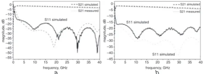
From the thickness fixed and the dielectric constant of the BCB polymer, we used the software Linecalc Agilent (ADS 2006 version) to determine the dimensions of the transitions in order to have a charac-teristic impedance of 50 V for both the MS and the GCPW sections: the width of the central strip is W ¼ 26 mm and the coplanar gap is G ¼ 13 mm. The length of the back-to-back transition with the CPW pads is fixed at 10 mm. For the second transition with rectangular stubs, the study is made for two lengths (L ¼ 10 mm and L ¼ 5 mm) to show the influence of the length on the bandwidth. The deposited aluminium (Al) thickness is 1.4 mm according to our measurement with a profil-ometer. The measured and calculated S-parameters of the transition with CPW pads are presented inFig. 2a. The experimental low and high 3 dB cutoff frequencies are 700 MHz and 22.5 GHz, respectively. The 3 dB high cutoff frequency is limited at 22.5 GHz because the inser-tion loss is greater than 1.8 dB, mainly due to the ohm effect in the thin Al layer. The transmission loss achieves 4.5 dB at 40 GHz because of the skin effect. The lower frequency limit of the bandwidth depends upon the surface of the coplanar pads. For applications such as radio over fibre, this lower frequency limit should be as low as possible[8]. This can be achieved by changing the topology of the first transition.
Fig. 2bshows the measurement and simulation S-parameter results of the transition realised with a rectangular stub. The experimental band-width extends from 200 MHz to 22.5 GHz. The lower frequency limit was improved without affecting the higher frequency. For realisation of this transition, we took L1 ¼ 1 mm and A ¼ 2.052 mm (A ¼ W+ 2× G + 2 mm). For the distance d between the end of the microstrip line and the inner part of the stub, we took 100 mm to avoid parasitic capacity between the signal and ground strips. The condition d . (W+ 2 × G) should be satisfied to limit this parasitic capacity accord-ing to[9]. The length of the coplanar ground plane L2 has been fixed to 500 mm so the applied driving signal in CPW mode can be stabilised and converted to MS mode.
0 –5 –10 –15 –20 –25 magnitude , dB –30 –35 –40 –45 –50 –55 0 –5 –10 –15 –20 –25 magnitude , dB –30 –35 –40 –45 0 5 10 15 20 a b S11 simulated S11 simulated S11 simulated S21 simulated S21 simulated S21 measured S21 measured frequency, GHz 25 30 35 40 0 5 10 15 20 frequency, GHz 25 30 35 40
Fig. 2 Measurement and simulation results of back-to-back GCPW-MS-GCPW transitions
a First structure with CPW pads b Second structure with rectangular stubs
0 –10 –20 magnitude , dB –30 –40 –50 0 –10 –20 magnitude , dB –30 –40 0 5 10 15 20 a frequency, GHz b frequency, GHz 25 30 35 S21 simulated S21 measured S11 simulated S11 simulated S21 S11 40 0 10 20 30 40 50 60 70 80 90 100
Fig. 3 Performance of transition with rectangular stub with L ¼ 5 mm a Measurement and simulation results
b Calculated S-parameters up to 100 GHz
For applications requiring short line lengths such as flip-chip intercon-nection[7], the bandwidth can be significantly improved. Measurement and simulation results of the transition with a rectangular stub with L ¼ 5 mm are presented inFig. 3a. Owing to the frequency limit of the used probe station, S-parameter measurements were limited to 40 GHz. But we can observe that the S21-parameter curve has a very low slope thanks to the very low loss tangent of the BCB polymer, and an ultra-wideband over 60 GHz could be expected. We also note perfect agree-ment between experiagree-mental and simulation results. To obtain this result, the excitation must be modelled by taking into account the probes used for characterisation. In HFSS software, we used the lumped port with the
exact parameters of our coplanar probes.Fig. 3bshows the simulation results of this transition beyond 40 GHz. A very wide bandwidth can be obtained. This bandwidth is only limited by the excitation of spurious resonance[10].
Table 1presents the performances of this transition as a function of the MS line length L and also the Al thickness. With L ¼ 5 mm, the bandwidth will be limited to 84 GHz even if the thickness of Al increases because of the excitation of the CPM (CPW MS) mode
[10]. With L ¼ 10 mm, this bandwidth can be significantly improved with 4 mm of Al thickness. In this case, a 78 GHz bandwidth can be obtained instead of 62 GHz with an Al thickness of 2 mm.
Table 1: 2 3 dB bandwidth of transition with rectangular stubs as function of length and metallisation thickness
L (mm) Thickness of Al (mm) Bandwidth 5 2 200 MHz – 84 GHz 3 4 10 2 200 MHz – 62 GHz 3 200 MHz – 75 GHz 4 200 MHz – 78 GHz
Analysis: The wide bandwidth of these transitions is achieved essen-tially thanks to four factors:
† The small thickness of polymer has a double advantage for a via-free transition. On the one hand, it can easily create an electromagnetic coup-ling between the bottom and top ground planes by capacitive effect. On the other hand, the low ratio between the BCB polymer thickness (10 mm) and the CPW gap G (13 mm) promotes the conversion of the field between CPW and MS modes.
† The low permittivity of the BCB polymer is a very important factor to achieve broad bandwidth. Indeed, the parasitic resonance between the backside conductor and the coplanar ground strips takes place at higher frequencies if the permittivity of the substrate is low[11]. † To decrease the lower frequency limit of the bandwidth, it is impor-tant to have a higher electromagnetic coupling. So, the surface of the CPW part should be as large as possible. However, the increase of this surface has drawbacks at high frequencies. Indeed, resonance modes appear at frequencies inversely proportional to the maximum size of the CPW part[10]. It is hence necessary to optimise the dimen-sions of the CPW part.
† Another important element is the low loss tangent of the polymer, especially at high frequencies. A good material must have a low permit-tivity and low loss tangent, which is the case of BCB polymer. Conclusions: We have presented ultra-wide bandwidth back-to-back transitions between GCPW and MS lines. Theses transitions based on BCB polymer are realised with an unpatterned bottom ground plane and without via-holes, which reduces the manufacturing steps and con-sequently the cost of components. The experimental bandwidth of these transitions is above 40 GHz with a lower limit frequency at 200 MHz. Simulation results showed that a very large bandwidth (84 GHz) could be achieved with the transition when L ¼ 5 mm, limited only by the excitation of the CPM mode, and 78 GHz when L ¼ 10 mm by
increasing the thickness of Al to 4 mm. These transitions are widely requested in component packaging, on-wafer measurements of MS based MMICs, and also in the interconnections in hybrid circuits includ-ing both a MS and a CPW.
Acknowledgments: The authors thank J.-P. Vilcot at the Institute of Electronics, Microelectronics and Nanotechnology of Lille for providing the BCB polymer. This work was supported by the ANR (French National Research Agency) through the project ModPol.
#The Institution of Engineering and Technology 2011 30 December 2010
doi: 10.1049/el.2010.3745
One or more of the Figures in this Letter are available in colour online. M. El-Gibari, D. Averty, C. Lupi, H. Li and S. Toutain (Institut de Recherche en Electrotechnique et Electronique de Nantes Atlantique (IREENA), Universite´ de Nantes, Nantes cedex 3 44322, France) E-mail: mohammed.elgibari@univ-nantes.fr
References
1 Kosslowski, S., Bertenburg, R., Koster, N.H.L., Wolff, I., Tegude, F.-J., Narozny, P., Wenger, J., and Dambkes, H.: ‘Advances in CPW-design applied to monolithic integrated Ka-band MESFET and HEMT-amplifiers on GaAs’. IEEE Gallium Arsenide Integrated Circuit (GaAs IC) Symp., 1992, Miami Beach, FL, USA, October 1992, pp. 119 – 122
2 Leib, M., Frei, M., and Menzel, W.: ‘A microstrip-fed ultra-wideband slot antenna’. IEEE Antennas and Propagation Society Int. Symp., 2009, Charleston, SC, USA, June 2009, pp. 1 – 4
3 Srisathit, K., Worapishet, A., and Surakampontorn, W.: ‘Design of triple-mode ring resonator for wideband microstrip bandpass filters’, IEEE Trans. Microw. Theory Tech., 2010, 58, pp. 2867 – 2877 4 Michalah, R., Kuo, Y., Nash, F., Szep, A., Caffey, J., Payson, P., Haas,
F., Mckeon, B., Cook, P., Brost, G., Luo, J., Jen, A., Dalton, L., and Steier, W.: ‘High speed AJL8/APC polymer modulator’, IEEE. Photonics Technol. Lett., 2006, 18, pp. 1207 – 1209
5 Ellis, T.J., Raskin, J.P., Katehi, L.P.B., and Rebeiz, G.M.: ‘A wideband CPW-tomicrostrip transition for millimeter wave packaging’. IEEE MTT-S Int. Microwave Symp. Dig., 1999, Anaheim, CA, USA, June 1999, pp. 629 – 632
6 Margomenos, A., Herrick, K.J., Herman, M.I., Valas, S., and Katehi, L.P.B.: ‘Isolation in three-dimensional integrated circuits’, IEEE Trans. Microw. Theory Tech., 2003, 51, pp. 25 – 32
7 Kim, J., and Itoh, T.: ‘A novel microstrip to coplanar waveguide transition for flip-chip interconnection using electromagnetic coupling’. 28th European Microwave Conf., 1998, Amsterdam, The Netherlands, October 1998, pp. 236 – 240
8 Garcia Larrode, M., Koonen, A.M.J., and Vegas Olmos, J.J.: ‘Overcoming modal bandwidth limitation in radio-over-multimode fiber links’, IEEE. Photonics Technol. Lett., 2006, 18, pp. 2428– 2430 9 Simons, R.N.: ‘Coplanar waveguide circuits, components and systems’
(John Wiley and Sons, 2001)
10 El-Gibari, M., Averty, D., Lupi, C., Li, H.W., and Toutain, S.: ‘Ultra-wideband GCPW-MS-GCPW driven electrode for low-cost and wide range application electro-optic modulators’, Microw. Opt. Technol. Lett., 2010, 52, pp. 1078– 1082
11 El-Gibari, M., Averty, D., Lupi, C., Brunet, M., Li, H.W., and Toutain, S.: ‘Ultra-broad bandwidth and loss GCPW-MS transitions on low-k substrates’, Electron. Lett., 2010, 46, pp. 931 – 933