HAL Id: tel-02132764
https://tel.archives-ouvertes.fr/tel-02132764
Submitted on 17 May 2019HAL is a multi-disciplinary open access
archive for the deposit and dissemination of sci-entific research documents, whether they are pub-lished or not. The documents may come from teaching and research institutions in France or abroad, or from public or private research centers.
L’archive ouverte pluridisciplinaire HAL, est destinée au dépôt et à la diffusion de documents scientifiques de niveau recherche, publiés ou non, émanant des établissements d’enseignement et de recherche français ou étrangers, des laboratoires publics ou privés.
hetero-epitaxial growth : Theory and Experiments
Ida Lucci
To cite this version:
Ida Lucci. Surface and interface contributions to III-V/Si hetero-epitaxial growth : Theory and Ex-periments. Physics [physics]. INSA de Rennes, 2019. English. �NNT : 2019ISAR0001�. �tel-02132764�
T
HESE DE DOCTORAT DE
L
’I
NSTITUTN
ATIONAL DESS
CIENCESA
PPLIQUEESR
ENNESCOMUE UNIVERSITE BRETAGNE LOIRE
ECOLE DOCTORALE N°596 Matière, Molécules, Matériaux
Spécialité : « science des matériaux»
« Surface and interface contributions to III-V/Si hetero-epitaxial growth:
Theory and Experiments »
Thèse présentée et soutenue à « l’INSA de Rennes », le « 26/02/2019» Unité de recherche : INSTITUT FOTON (UMR 6082 / CNRS)
Thèse N° : 19ISAR 02 / D19 - 02 Par
« Ida LUCCI »
Rapporteurs avant soutenance :
Pierre MULLER
Professeur, CINaM, Université d'Aix Marseille
Magali BENOIT
Directrice de recherche CNRS, CEMES, Toulouse
Composition du Jury :
Président Jean-Christophe HARMAND
Pierre MULLER
Professeur, CINaM, Université d'Aix Marseille/ Rapporteur Magali BENOIT
Directrice de recherche CNRS, CEMES, Toulouse / Rapporteur
Kerstin VOLZ
Professor, Philipps-Universität Marburg / Examinateur Jean-Christophe HARMAND
Directeur de recherche CNRS, C2N / Examinateur Charles CORNET
MCF HDR, Institut FOTON, INSA de Rennes / Directeur de thèse
Laurent PEDESSEAU
MCF, Institut FOTON, INSA de Rennes / Co-encadrant de thèse
Pascal TURBAN
Intitulé de la thèse :
Surface and interface contributions to III-V/Si hetero-epitaxial growth: Theory and Experiments
Ida LUCCI
En partenariat avec :
First of all, I want to thank my thesis supervisors Charles Cornet, Laurent Pedesseau and Pascal Turban for giving me the chance to pursue my Ph.D. as part of the ANTIPODE project.
I felt very lucky to be advised and supported by Charles during these years. Thanks to his advice I was able to get through the many difficulties encountered during my Ph.D. I really appreciated his availability for helping me when needed and his ability to transfer to me his knowledge. Thanks to Laurent, for always supporting me and also for introducing me to the Density Functional Theory (DFT) world. Without his support, I would not have been able to overcome the complex calculations-related obstacles I went through during my Ph.D.
Thanks to both of you for your suggestions, all the meetings (with a lot of good laughs too). This experience will be a solid starting point for a new exciting chapter of my life.
Thanks to Pascal Turban and my colleague Simon Charbonnier for their useful contributions to my Ph.D. work.
Thanks to the committee members Jean-Christophe Harmand, Magali Benoit, Pierre Muller and Kerstin Volz for their questions and suggestions for improving my thesis work.
Thanks to all the members of the ANTIPODE project I worked with. It was a pleasure for me to meet you and share each time ideas to advance my research. In particular, I want to thank Anne Ponchet who gave me precious advice for improving my thesis work results.
I want to thank also Rozenn Gautheron-Bernanrd for the help and everything you taught me during the experimental part of my work. I felt very lucky to have the chance to work with you.
I learned how important is to work with people who transmit their curiosity, their passion for learning and their creativity. You have definitely been one of them for me.
I want to thank Thomas for the nice talks about football and do not forget always FORZA NAPOLI!. I also want to thank Isabelle and Alexandrine for having shared some really funny moments together which made easier for me to spend hard work days in the lab.
I want to thank all my colleagues Gaelle, Alejandro, Daniel, Tore and Michael for the nice time together and in particular I want to thank Ronan, the best colleague for sharing the office with. We helped each other, we shared ideas and we also spent funny moments together. Thank you for having been a friend more than a simple colleague at work.
Finally, I want to thank all the Foton institute members for the nicest work environment where I could have ever spent four years of my life starting with an internship and finishing as a Dr. No àit sàti eàtoàs it hài àItalia àfo à àfa il àa dà àItalia àfa il ài à‘e es.
Grazie ai miei genitori e mia sorella sempre pronti a supportarmi durante tutti i miei traguardi raggiunti nonostante la lontananza e grazie per il loro amore incondizionato. Grazie ai miei
Grazie alla mia amica Lavinia per aver sempre creduto in me.
Grazie a tutti gli amici di Rennes. In particolare, Arianna, Claudia e Melania con le quali ho condiviso tante risate e tanto affetto riuscendo a formare un legame speciale in così poco tempo. Grazie a Khaled e Francesca per avermi fatto rivivere momenti di spensieratezza donandomi attimi di pausa dal duro lavoro. Grazie ad Elena e Raimondo per tutte le serate in super stile italiano (soprattutto per le pizze). Grazie per la vostra continua disponibilità, siete delle persone speciali. Un grazie particolare va alla mia piccola famiglia di Rennes (o meglio il G uppoà u ito à “teph,à ‘i a do,à ‘osaà e Fausta. Loro, il mio anti-stress. Grazie per tutti i bellissimi momenti insieme.
Voglioài fi eà i g azia eà ioà a itoàFa izio,àlaà iaàfo zaàeàlaà iaàispi azio e.àE àa heàg azieàaà lui se sono arrivata fin qui. Lui che mi è accanto da 12 anni e che mi ha sempre supportata. Grazie per essermi stato sempre vicino, per credere in me e nelle mie potenzialità.
E àstataàu aà ellissi aàespe ie za.à Grazie, merci à tous!
i
General introduction ... 1
Chapter 1 : III-V on silicon for photonics and energy applications ... 5
1.1. Silicon: a material with limited optical properties ... 5
1.2. III-V/SI integration approaches ... 7
1.2.1. Hybrid integration ... 8
1.2.2. Monolithic integration ... 11
1.2.2.1. Metamorphic integration ... 12
1.2.2.2. Pseudomorphic integration ... 16
1.3. Monolithic integration challenges: III-V/Si interfacial issues ... 17
1.3.1. Surface preparation ... 17
1.3.2. Lattice mismatch and thermal expansion coefficient ... 18
1.3.3. 3D-growth... 20
1.3.4. Polar on non-polar epitaxy ... 21
1.3.4.1. Stacking faults and microtwins ... 21
1.3.4.2. Antiphase domains ... 22
1.4. Conclusions ... 25
Chapter 2 : Surface and Interface energies by density functional theory ... 33
2.1. Introduction to density functional theory ... 33
2.1.1. Hohenberg-Kohn theorem ... 34
2.1.2. Kohn-Sham approach ... 35
2.1.3. The LDA approximation ... 35
2.1.4. The GGA approximation ... 36
2.1.5. Self-consistent total energy and relaxation calculations ... 36
2.1.6. Siesta Code: basis sets, pseudopotential and k-points ... 37
2.2. General surface energy equation ... 39
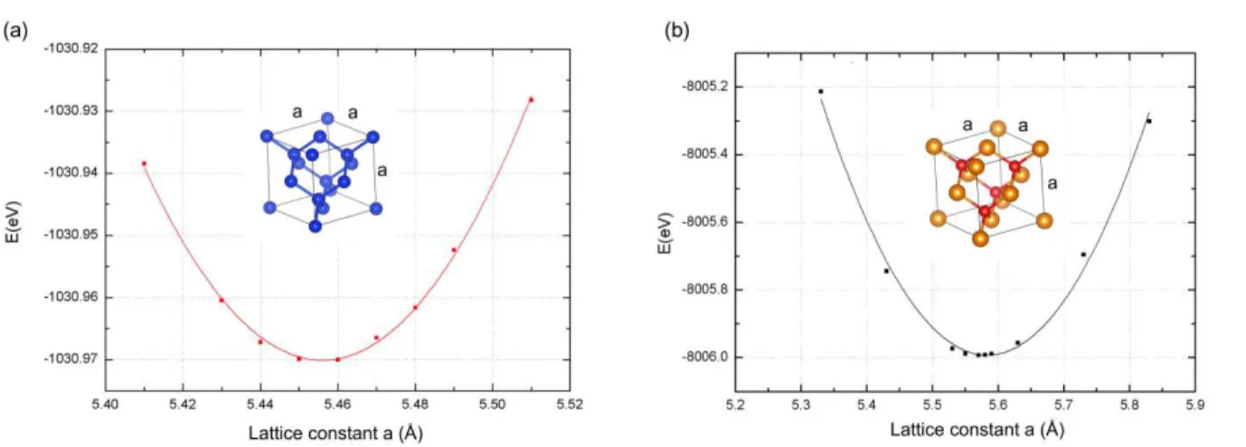
2.3. Si and GaP bulk ... 39
2.4. Silicon surface ... 39
2.4.1. Common computational details and surface energy calculations ... 40
2.4.2. Flat Si(001) surface reconstruction ... 41
2.4.3. Stepped Si(001) surface... 43
ii
2.4.4. Energies of the flat Si(001) with and without steps ... 44
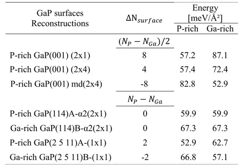
2.5. Polar and non-polar GaP surfaces ... 46
2.5.1. Electron counting model ... 46
2.5.2. Common DFT computational details ... 48
2.5.3. Chemical potential ... 48
2.5.4. Non-polar GaP(001) surfaces ... 50
2.5.4.1. GaP(001) surface reconstructions ... 50
2.5.4.2. GaP(001) surface energies ... 51
2.6. Polar GaP(114) and GaP(136) surfaces ... 52
2.6.1. GaP(114) and GaP(2 5 11) surface reconstructions ... 53
2.6.2. Fictitious H*-passivation approach ... 55
2.6.3. H*-passivation approach applied to GaP(114) and GaP(2 5 11) surfaces ... 57
2.7. GaP(001), GaP(114) and GaP(2 5 11) surface energies ... 58
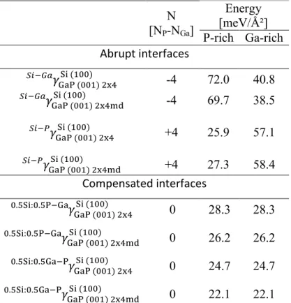
2.8. GaP/Si interface energies ... 60
2.8.1. DFT common computational details ... 62
2.8.2. Compensated interfaces ... 62
2.8.3. Abrupt and compensated interface energies calculation ... 65
2.9. Conclusions ... 68
Chapter 3 : Description of III-V/Si epitaxial growth processes ... 73
3.1. State-of-the-art ... 73
3.1.1. 3D islanding of different III-V/Si systems ... 74
3.1.2. Solid wetting theory applied to GaP/Si ... 79
3.2. Free-energy calculations from the equilibrium shape given by the Wulff-Kaishew theorem ... 82
3.2.1. Wulff-Kaishew theorem applied to GaP/Si system ... 86
3.2.2. Total free energy variation during the GaP/Si epitaxial growth ... 90
3.3. General description of the III-V/Si epitaxial growth ... 93
3.4. Conclusions ... 96
Chapter 4 : Silicon growth and surface control for III-V/Si integration ... 99
4.1. Si(001) surface chemical preparation and growth by UHV-CVD ... 99
4.1.1. Si(001) surface treatments ... 100
iii
4.2. Toward a contamination-free Si(001) surface ... 106
4.2.1. Annealing of Si(001) under an H2 or SiH4 atmosphere... 108
4.3. Silicon surface reconstruction vs growth conditions ... 111
4.4. Antiphase boundaries in GaP/Si epitaxial layers ... 116
4.4.1. APDs annihilation ... 116
4.4.2. APBs electrical characterization ... 120
4.5. Conclusions ... 121
Chapter 5 : Surface texturation of GaP on Si for water splitting applications ... 127
5.1. Introduction to PEC water splitting ... 127
5.2. GaP and PEC water splitting devices ... 131
5.3. Experimental results ... 131
5.4. GaP textured surface on Si vicinal substrate ... 132
5.5. AlSb/GaP(001): texturation without vicinality ... 135
5.6. DFT computational details ... 136
5.7. Textured surface on Si, over a 2-inch wafer ... 139
5.8. Benefits of using the stress-free nanopatterned GaP(114)A surface for water splitting applications ... 141
5.9. Conclusions ... 142
Conclusions and perspectives ... 147
Perspectives... 149
Appendices ... 150
A. Density functional theory (DFT) ... 150
B. Molecular beam epitaxy and ultra-high vacuum chemical vapor deposition ... 152
C. Atomic force microscopy ... 155
D. Reflection high energy electron diffraction ... 158
Résumé ... 164
1
General introduction
Silicon photonics, which consists in the integration of photonic components and circuits on Silicon On Insulator (SOI) wafers, comes from the idea of applying the benefits of low-cost silicon manufacturing to photonics. It also aims to overcome the electrical interconnections limits by on-chip and intra-chip high speed optical communications. Since the pioneering work of Soref et al. in 1985 [1], the silicon photonics researches have been boosted with the realization of many integrated photonic devices, such as modulators or photodetectors. A major advance in the CMOS integrated nanophotonic technology was reported in 2012 by IBM, integrating side-by-side in a 90nm fabrication process electrical and optical components [2]. So far, the integration of lasers on chip is still a challenge. Nevertheless, in the context of the photonics integrated on chip, the III-V on Si co-integration is a strategy proposed to improve the photonic devices performances [3]. Indeed, it combines the good optical properties of III-V semiconductors with the mature silicon technology [4]. Especially, the monolithic approach is a very promising integration technique, as reminded in 2018 by INTEL (ECOC conference). Indeed, it allows the direct growth of III-Vs on silicon i àaà f o t-e d às he eà ithàtheàad a tageàto be compatible with very large scale integration (VLSI) applications [4]. Nevertheless, it has to face different challenges such as defects formation due to the III-V/Si lattice mismatch, or the formation of antiphase domains (APDs) due to the epitaxial growth of polar-III-Vs on non-polar silicon [5]. Thus, even if III-V/Si templates are already commercially available at the NAsP for instance [6] the control and understanding of defects generation and propagation at the early stage of III-V/Si growth is a subject of interest for a lot of research groups.
Thisàthesisàisàpa tàofàtheà Advanced aNalysis of III-V/Si nucleaTIon for highly integrated PhOtonic Devices
(
ANTIPODE) project (supported by the French National Research Agency – Grant No. 14-CE26-0014-01), which aims to deeply understand what happens during the initiation step of the III-V epitaxy on Si. Especially, it should clarify the interplay between 3D-growth mode, strain relaxation and APDs generation. Thus, the ANTIPODE project main objectives are the understanding of: (i) the 3D nucleation mechanism of III-V semiconductors on silicon (including generation of defects during coalescence) and the associated strain2
relaxation mechanisms (ii) the nature and role of the interfacial charges on the growth and defects generation (iii) the influence of the initial silicon surface.
In the context of the ANTIPODE project, this thesis focuses especially on the GaP on Si 3D-growth. Such a system, because of its low lattice mismatch (0.3%), is interesting for photonics and photovoltaic applications [7]–[9]. Nevertheless, antiphase domains are a big issue limiting the GaP-based devices performances [5], [9]–[12]. Thus, the thesis aims i) to determine, by density functional theory (DFT) calculations, the absolute surface and interface energies in the GaP/Si materials system, ii) to understand their role in the GaP/Si 3D-growth mode and iii) to compare these energy values with other III-V-based on Si systems. Finally, it aims to study experimentally the silicon surface structure for subsequent III-V overgrowth.
Dissertation overview:
Chapter 1 presents the state-of-art of different III-V on Si integration approaches and photonic
and photovoltaic devices developed through the different integration techniques. The monolithic integration of III-V semiconductors on Silicon and its challenges (such as lattice mismatch and defects formation) are presented. Finally, a particular attention is given to the antiphase domains showing the works performed by different research groups to try to control or annihilate them.
Chapter 2 presents the atomistic simulations performed by DFT to determine the absolute
surface and interface energies of the GaP/Si(001) system. Si(001) surface energies are first determined. Then, GaP non-polar (001) and polar (114) and (136) surface energies are computed. Finally, both abrupt and compensated absolute GaP/Si interface energies are determined.
Chapter 3 aims to clarify the main steps at the very early stage of the III-V on Si growth. For this
reason, three different III-V/Si materials systems presenting 3D-monodomain islands morphologies are first studied. The GaP/Si wetting properties are investigated on the basis of surface and interface energies determined by DFT calculations over the full range of phosphorus chemical potential, as showed in Chapter 2. The contributions of these energies and of the elastic relaxation of strain, to free energy change during the III-V/Si epitaxy are compared.
3 Finally, the main steps of the III-V/Si 3D-growth and the defects generation by coalescence are clarified.
Chapter 4 focuses on finding experimentally new strategies for developing a Si(001) surface
compatible with III-V overgrowth. Thus, we investigate strategies to control the silicon surface steps organization and to protect the silicon surface from contaminants. Different growth parameters are varied for achieving a monodomain silicon surface on nominal and vicinal Si(001) substrates. Furthermore, GaP samples were grown on the same silicon substrate to study the efficiency of a thin AlGaP marker layers to control APDs vertical propagation. Finally, preliminary results on the electrical properties of antiphase boundaries are presented.
Chapter 5 focuses on the context of energy conversion applications such as the
photoelectrochemical (PEC) water splitting. Indeed, the formation by surface energy engineering of textured GaP templates, monolithically grown on Si, is investigated. This study is supported by experimental results and DFT calculations presented in Chapter 2. The advantages of using such a textured surface in the PEC water splitting application are also discussed.
References
[1] ‘.àá.à“o efàa dàJ.àP.àLo e zo,à “i gle-crystal silicon: a new material for 1.3 and 1.6 µm integrated-opti alà o po e ts ,àElectronics Letters, vol. 21, no. 21, pp. 953–954, Oct. 1985. [2] S. Assefa et al.,à áà m CMOS integrated Nano-Photonics technology for 25Gbps WDM
opti alà o u i atio sàappli atio s ,ài àElectron Devices Meeting (IEDM), 2012 IEEE
International, 2012, pp. 33.8.1-33.8.3.
[3] D. T. Spencer et al.,à á àopti al-frequency synthesizer using integratedàphoto i s. ,àNature, vol. 557, no. 7703, pp. 81–85, May 2018.
[4] C. Cornet, Y. Léger, and C. Robert, Integrated Lasers on Silicon. ISTE-Elsevier, 2016. [5] H.àK oe e ,à Pola -on- o pola àepita ,àJ. Cryst. Growth, vol. 81, no. 1–4, pp. 193–204,
Feb. 1987.
[6] á outàusà- NásP .à[O li e].àá aila le:àhttps:// . asp.de/a out_us.ht l.
[7] E.àE.àBa to ,àD.àM.à‘a pulla,àa dàá.àB.àBo a sl ,à “ele ti eà“ola -Driven Reduction of CO2 to Methanol Using a Catalyzed p-GaPàBasedàPhotoele t o he i alàCell ,àJ. Am. Chem. Soc., vol. 130, no. 20, pp. 6342–6344, mai 2008.
[8] O. Supplie, M. M. May, H. Stange, C. Höhn, H.-J.àLe e e z,àa dàT.àHa appel,à Mate ialsàfo à light-induced water splitting: In situ controlled surface preparation of GaPN epilayers grown lattice- at hedào à“i ,àJournal of Applied Physics, vol. 115, no. 11, p. 113509, Mar. 2014.
4
[9] K. Volz et al.,à GaP- u leatio ào àe a tà“ià à à àsu st atesàfo àIII/Vàde i eài teg atio ,à
Journal of Crystal Growth, vol. 315, no. 1, pp. 37–47, Jan. 2011.
[10] á.àC.àLi ,àM.àM.àFeje ,àa dàJ.à“.àHa is,à á tiphaseàdo ai àannihilation during growth of GaP o à“ià à ole ula à ea àepita ,àJournal of Crystal Growth, vol. 363, pp. 258–263, Jan. 2013.
[11] E. Tea et al.,à Theo eti alàstud àofàopti alàp ope tiesàofàa tiàphaseàdo ai sài àGaP ,àJournal
of Applied Physics, vol. 115, no. 6, p. 063502, Feb. 2014.
[12] O. Supplie et al.,à áto i às aleàa al sisàofàtheàGaP/“i àhete oi te fa eà ài àsituà efle tio àa isot op àspe t os op àa dàa ài itioàde sit àfu tio alàtheo ,àPhys. Rev. B, vol. 90, no. 23, p. 235301, décembre 2014.
5
Chapter 1 : III-V on silicon for photonics and
energy applications
In the following chapter we provide an overview of the III-V on Si devices developed so far through different integration techniques. To this aim, we first explain the interest in growing III-V semiconductors on Si. Then, we explain the different integration approaches which are hybrid and monolithic. Finally, we will thoroughly describe the main challenges of the monolithic integration approach due to crystal defects at the III-V/Si interface that can deteriorate the device performances.
1.1. Silicon: a material with limited optical properties
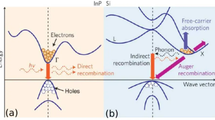
Figure 1.1 Energy bandgap diagram of (a) direct bandgap semiconductors, e.g. InP
semiconductor, where electrons-holes recombinations take place transferring the energy to emitted photons (b) indirect semiconductors, e.g. Si semiconductor, where the little photon emission is a result of the co-existence of electrons-holes recombinations, assisted by the
absorption or emission of phonons, together with Auger recominations. Courtesy of [1]
The main reason why silicon is not a good light emitter material is because of its electronic structure which features an indirect band gap, leading to inefficient radiative recombination. Indeed, light emission happens when an electron from an excited state moves
6
to a lower energy state, in other words, it radiatively recombines with a hole by emitting a photon. It happens in direct bandgap semiconductors, where the lower energy level of the conduction band and the higher energy level of the valence band correspond to the same wave vector value. It is called zero momentum point. Instead, for indirect bandgap semiconductors, the probability that recombination happens is very low because it requires a phonon-assisted transition in order to satisfy the momentum conservation as shown in Figure 1.1. It is the case of silicon, where the X valley, which corresponds to the lowest energy of the conduction band, is not aligned with the point corresponding to the maximum energy of the valence band. This results in a poor internal quantum efficiency of light emission in Si and also, in limited optical absorption properties. In contrast to silicon, many III-V compounds are direct band-gap semiconductors such as GaAs, or InP. This physical property of semiconductors is a main concern for different applications. Indeed, in the general context of integrated photonics on chip, the silicon material cannot be used to develop an efficient laser source, while III-V semiconductors are the materials of choice.
For photovoltaic applications crystalline silicon is also not the most efficient material due to its indirect bandgap that provides, in addiction to slow recombination and a long charge carrier lifetime, low absorption properties. Nevertheless, high efficiency silicon based solar cells have been developed, with 26.7% record efficiency achieved by Kaneka in early 2017, see ref. [2] and references therein for instance. On the other hand, the III-V direct bandgap is translated into a very short absorption distance and high photocurrent. Moreover, the III-V compounds bandgap can be tuned to improve the solar cells quality. Efficiency up to 46% for III-V multijunction concentrator solar cells has been recently achieved [3], [4]. Nevertheless, their high costs limit their applications. Thus, III-V on Si integrated solar cells have been studied in order to drastically lower the costs while achieving a comparable efficiency [5]–[7]. Thus, many research efforts were given in the last 20 years on the integration of III-V semiconductors on Si substrate.
7
1.2. III-V/SI integration approaches
Many different strategies were used to co-integrate III-V semiconductors and silicon in the field of photonics and energy. To illustrate this idea, we will here show some of the advanced integration strategies that have been developed in the field of on-chip integration of photonics. In order to combine the high technology of silicon-based integrated circuits (ICs) with III-V-based components realizing photonics integrated circuits (PICs) on silicon, different integration schemes have been developed. Three of them are: front-side, front-end and back-side. They are shown in Figure 1.2
Figure 1.2 Three schemes to integrate photonic layer and CMOS technology. Courtesy of [8]
In the front-side scheme, the photonic devices are embedded in the last level of the metallization pattern of the complementary metal-oxide semiconductors (CMOS) fabrication process. This scheme enables off-chip optical communications. Nevertheless, beside the additional costs needed to introduce some modifications to the CMOS fab-line, it may reduce the thermal budget of the electronics due to the additional layer added on the top thermal path [8], [9]. The back-side scheme, proposed in the pHotonics ELectronics functional Integration on CMOS (HELIOS) project [10], consists in integrating the photonic devices on the substrate backside. The connections between CMOS and photonic layer are achieved by through-silicon-vias (TSV). In both the approaches explained above, the electronic and photonic parts can be processed independently. The front-end scheme allows the fastest connection between the photonic components and CMOS technology due to their vicinity. This scheme was realized by Luxtera [11], MIT [12] and IBM [13]. In this case, all components are fabricated at the same time. Thus, it increases the process complexity.
For each strategy, basically two integration paths may be considered. The hybrid one, hi hà o sistsài à sti ki g ào à o di g àopti alàla e sào àde i esàdi e tl ào àtheàsili o à hip,ào à
8
the monolithic one, which consists in growing epitaxially photonic devices on the silicon, and process it afterwards to define the photonic layer. In particular, front-side and back-side schemes are compatible with hybrid integration while the front-end scheme is more adapted to the monolithic integration approach. The principle of hybrid and monolithic integration approaches will be described in the next sections.
1.2.1. Hybrid integration
The hybrid approach consists in bonding the III-V semiconductors on Si or Silicon On Insulator (SOI) platforms (at the wafer or die level). The bonding process can be achieved by direct bonding (molecular-assisted), adhesive bonding (polymer-assisted) or metal-assisted bonding.
The molecular-assisted bonding is based on Van der Walls intermolecular forces and hydrogen bonds. A proper surface cleaning, before the bonding process, is necessary for promoting a flat and clean substrate in order to have a high-quality III-V on Si interface. Then, the surface is chemically treated to be either hydrophobic (-H terminated) or hydrophilic (-OH terminated). After that, the bonding process occurs. The two wafers are bonded via hydrogen bonds independently of the kind of surface treatment. Finally, thermal annealing permits to strengthen the bonding in order to achieve stable and permanent bonds at the interface [8]. In 2006 A. W. Fang et al. of the Bowers group [14] realized a hybrid laser where the III-V quantum wells (QWs) layers are connected to the SOI waveguides by O2 plasma-assisted
molecular bonding. The system is based on an evanescent coupling where the optical mode is mainly confined in the SOI waveguide (75%) and interacts just for a few percentage (3%) with the III-V semiconductor layers [14]. The device scheme is shown in Figure 1.3. This continuous wave laser presents, at room temperature, a threshold current of 65mA and an output power on the order 1.8mW [14]. The same group improved the device performances by reducing of 30%-40% the threshold current density and threshold voltage. Moreover, they showed that the overlap of the optical mode with the III-V QWs layer can be tailored as a function of the waveguide dimensions [15].
9
Figure 1.3 Schematic drawing of the hybrid laser structure developed by Bowers group.
Courtesy of [14]
Another kind of hybrid integration is the polymer-assisted bonding or adhesive bonding. This technique is less limiting with respect to the molecular bonding, on the surface roughness. Nevertheless, the surface cleaning is always the first step before the bonding process. Benzocyclobutene (BCB) is a typical polymer used for achieving the bonding. It is first spin-coated on the SOI wafer then, it is baked at 150°C to evaporate the solvent. Indeed, it is applied to the wafer, before the spin-coating, to improve the adhesion of the polymer. After the BCB polymerization, the structure is cooled down to form a solid well-bonded device [8]. A Fabry-Pérot cavity laser based on this approach, was realized by IMEC-Ghent University group in 2006 [16] (Figure 1.4). As in the case mentioned above [14], the optical mode is mainly present in the Si waveguide. Moreover, 300nm-thick BCB connects the III-V layers to the inverted tapered SOI waveguide where light coupling occurs. The device presented a high threshold current (150mA) in a pulsed mode. One of the reasons of this high value was the high thickness of the BCB layer [16]. Stankovic et al.[17], [18] improved the system by realizing a Fabry-Pérot laser bonded to the Si substrate through a thinner adhesive BCB (40-50nm).
The heterogeneous bonding is another example of hybrid integration. It differs from the structures presented just above, because of the optical mode which is mainly confined in the III-V layers. Lamponi et al.[19] first presented such a laser by realizing a InP/SOI laser integrated by adhesive bonding approach. It presents a threshold current of 30mA at 20°C and a maximum output power of 4mW [19], [20]. The novelty of the system is the development of a double tapered region which enhances the coupling efficiency of nearly 95% [20]. The scheme is presented in Figure 1.5(a). Another laser structure (Figure 1.5(b)) based on the heterogeneous
10
approach is the microdisk integrated on the SOI waveguide either by molecular or polymer-assisted bonding [21]. The III-V microdisk experiences a whispery gallery mode which is evanescently coupled to the SOI waveguide. Their shallow threshold current (0.45mA achievable with a diameter of 7.5µm) [23] and their compact size make the microdisk lasers very promising for on-chip interactions [23], [24].
Figure 1.4 Scheme of the Fabry-Perot laser adhesive bonded to the SOI waveguide. Realized by
the IMEC-Ghent University group [16]
Figure 1.5 Heterogeneous integration based devices: (a) scheme of InP double tapered laser
developed by Lamponi et al.[19] (b) scheme of a InP microdisk presented by [22]
The last approach presented in this paragraph is the metallic bonding strategy which consists in using a metal alloy with a specific eutectic point. The metal alloy is deposited on the wafers and it melts when the system is heated up at a temperature greater than the eutectic
11 one. Once melted, the metal will cover all the bonding area and when the temperature is cooled down, a strong bond is realized through its solidification. The metal alloy choice depends on different factors such as its eutectic point, the thermal expansion coefficient of the III-V semiconductors and the thermal budget of the bonding post-processing steps. Lasers structures based on this approach were proposed in [25]–[27].
In the field of photovoltaics, high efficiencies have been achieved through wafer bonded III-V/Si solar cells, such as 32% being the current record for Si-based two-junctions solar cells and 35.9% for three junctions III-V//Si solar cells under one-sun illumination fabricated by NREL and CSEM [6] while 33% for a two-terminal III-V//Si triple-junction cell under 1-sun AM1.5G was recently obtained in [5]. Instead, FhG-ISE, SOITEC, CEA-LETI [3] jointly developed a four-junction solar cell, obtained growing a GaInP/GaAs//GaInAsP/GaInAs cell on InP substrate, with a record efficiency of 46% at 312xAM1.5d.
1.2.2. Monolithic integration
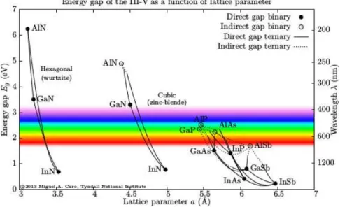
The monolithic integration consists in growing the III-V semiconductors directly on Si substrate. This approach has different advantages with respect to the hybrid one, such as low fabrication costs and time. It also enables the very large scale integration of III-V devices on Si which cannot be achieved through the hybrid integration. Nevertheless, the primary challenge is to reach a high III-V/Si interface crystal quality. In the plot of Figure 1.6 the bandgap energies of different III-Vs are presented as a function of their lattice constant. It shows that III-V alloys such as GaAs, GaSb or InP, typically used in this approach, have a direct bandgap but a large lattice mismatch to the silicon. It can cause defects formation, decreasing the system efficiency. On the other hand, III-Vs such as AlP or GaP are quasi-lattice-matched to the silicon but, they have an indirect bandgap which can limit as well the device performances. In particular, when growing lattice mismatched III-Vs on Si substrate the integration is called metamorphic, otherwise it is pseudomorphic. These integration approaches and the strategies used to overcome the related growth issues are presented in the following paragraphs.
12
Figure 1.6 Plot of the energy gap as a function of the lattice parameter of binary III-V
semiconductors. Courtesy of [28]
1.2.2.1. Metamorphic integration
The metamorphic approach consists in the mismatched epitaxial growth of III-V semiconductors on silicon substrate. The main advantage of III-V semiconductors, such as GaAs or InP, is their low and direct bandgap but, as introduced just above, they present a large lattice mismatch to the silicon. As a consequence the dislocations formation is unavoidable. These defects act as non-radiative recombination centres in the structure. Thus, their density has to be minimized (< 104cm-2) to increase the device performances. Figure 1.7 shows an example of dislocations distribution in a GaAs on Si epilayer [29].
In order to improve the device performances, tremendous efforts have been done to grow high quality III-V epitaxial layers on Si substrate. One approach consists in the self-organization of dislocations when using for example Sb-based compounds which have a very large lattice mismatch to the Si (such as GaSb 12% or AlSb 13%). Indeed, strain energy due to the large mismatch is immediately relieved into the III-V epilayer by the formation of interfacial misfit dislocations (IMD) arrays [30], [31]. An example is given by the growth of AlSb on Si substrate which results in the formation of planar array of 90 ° misfit dislocations partly confined at the interface as shown in Figure 1.8. The very low threading dislocation density
13 (~7x105cm-2)achieved though this growth procedure highlights the potential of this approach in the monolithic integration. Kim et al. and Akahane et al. [32], [33] improved the crystal quality of the GaSb/Si interface by using an AlSb nucleation layer. Indeed, GaSb-based devices have also been realized in [34], [35].
Figure 1.7 Cross-sectional TEM image of dislocations propagating through the GaAs grown on Si.
Courtesy of [29]
Figure 1.8 Cross-sectional HRTEM image of planar 90° misfit array at the AlSb/Si interface.
Courtesy of [30]
Another effective strategy to reduce the threading dislocations is the use of strained layer superlattice (SLS) and short period superlattice (SPL) [36]. The effectiveness of this approach has been demonstrated by growing high quality InGaAs quantum-dots (QDs) on Si
14
substrate and also by growing InP-on-Si heterostructures [29], [37]. An example of this approach is shown in Figure 1.9.
Figure 1.9 Cross-sectional TEM image showing the suppression of threading dislocations
through the grow of strained superlattice (SPS) and short period superlattices (SPL). Courtesy of [29]
Another approach highly investigated is the adaptation of the lattice parameter by compositionally graded buffers, such as SixGe(1-x)/Si pseudo substrate [38] to reduce the
dislocation density at the GaAs/Si interface. High performance GaAs-based solar cells [39] and laser structures [40] have been realized. This strategy was also used to grow lattice mismatched GaAs0.7P0.3 solar cells on Si substrate [41].
The selective-area-heteroepitaxy is another approach for controlling the propagation of dislocations by using masks which restrict the III-V growth in pre-defined areas. An example is called selective area growth (SAG) where dielectric masks (typically made by SiO2) are formed by
small windows (of the order of dozens to hundreds of nanometres [42]–[44]) at the silicon substrate. The III-V overgrowth will occur in these openings taking advantage of the defect necking effect [45]. It makes dislocations trapped in tranches in between two SiO2 walls. The
effectiveness of this approach is illustrated in Figure 1.10 where a InP nanolaser has been grown on Si(001) substrate by etal−o ga i à he i alà apo àdepositio process (MOCVD) [42]. In this
15 case, the mask is fabricated by deposing, through the Shallow-Trench-Isolation (STI) process, SiO2 forming 100nm-thick tranches used for the III-V overgrowth. In order to reduce the lattice
mismatch related to the III-V on Si deposition, before the overgrowth, a Ge seed layer is grown in the openings on the Si substrate.
Figure 1.10 Cross-section scheme of the SAG approach used to grow the InP nanolaser to the Si
substrate. Courtesy of [42]
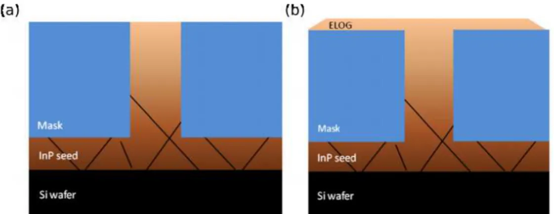
Another kind of selective growth, which is considered as a special case of SAG, is the epitaxial lateral overgrowth (ELO). It consists in growing the III-V semiconductors directly on Si substrate. The high density of dislocations (of the order of 109cm-2 due to the large lattice mismatch [46]) is then filtered by the deposition of a patterned mask whose windows are defined for the subsequent III-V lattice matched epitaxial overgrowth [46], [47]. Smaller is the thickness of the mask windows, less is the chance of the threading dislocations to pass through them, benefiting from theà e kli gàeffe t [45]. An example is the InP ELO on Si using a SiO2
mask in Figure 1.11.
Growing III-V on a V-groove Si(001) substrate has demonstrated its efficiency in the improvement of the GaAs/Si interface quality by reducing the dislocation density and also by growing antiphase domains (APDs)-free III-V layers [48]–[50].
Finally another strategy largely used is the growth of III-V on Si nanowires generally considered to be APDs-free [51]. It consists in growing III-V core-shell nanowires through catalyst–assisted (such as catalyst Au nanoparticles) or a catalyst-free processes [52], [53].
16
In the photovoltaics context, a quadruple-junctions inverted metamorphic (4J-IMM) solar cell was developed in 2015 by NREL with an efficiency of (43.8 ± 2.2)% at 327-sun concentration [4].
Figure 1.11 Scheme of the ELO growth process of InP layer grown on Si wafer: (a) defect-necking
effect and (b) epitaxial lateral overgrowth. Courtesy of [47]
1.2.2.2. Pseudomorphic integration
The pseudomorphic integration consists in growing III-V semiconductors lattice matched on the Si substrate, in order to avoid the formation of misfit dislocations for achieving a perfect crystalline quality. The low lattice mismatch between the III-Vs (such as GaP and AlP) and the silicon surface allows avoiding misfit dislocations formation until a critical thickness of around 100 nm. One of the best candidates for this approach is definitively the GaP. Indeed, thanks to its very low lattice mismatch (0.37%) to the Si, good atoms alignments [54] can be achieved as shown in Figure 1.12(a). By choosing the right growth conditions, it is possible to avoid defects formation such as microtwins (MTs) and to annihilate antiphase domains [55] as shown in
Figure 1.12(b) where most of the antiphase boundaries (APBs) are annihilated within 10 nm
from the GaP/Si interface. Nevertheless, the performances of GaP-based laser devices are limited by the indirect nature of its band structure. Many materials developments were published with the aim of achieving high structural quality. For instance, Takagi et al. [56] were able to reduce the defects formation and to improve the surface roughness by migration enhanced epitaxy (MEE). Volz et al. [57] were able to grow a defect-free GaP/Si(001) after
17 almost 50 nm GaP layer thickness. Also, Grassman et al. presented a two-step growth process consisting in growing GaP on Si(001) by low temperature MEE followed by molecular beam epitaxy (MBE) [58]. In this way, they were able to achieve a very smooth and defect-free GaP/Si interface. Lasing on Silicon was even demonstrated with GaAsPN quantum wells [59]. In order to overcome the band structure problem, it has been demonstrated that the incorporation of Nitrogen (N) can convert the GaP indirect bandgap into a pseudo direct one. Moreover, by taking advantages from the V-N compounds lattice matched to the silicon, dislocation-free III-V-N-based QWs structures, such as GaAsyP1-x-yNx /GaP0.98N0.02, can be formed with a percentage
of N typically less than 3% [60], [61].
Figure 1.12 Cross-secton (a) HRSTEM-HAADF image of GaP grown on Si hilighting the good
atoms alignment at the interface. Courtesy of [54] (b) STEM-BF image hilighting the annihilation of APDs at 10nm from the interface. Courtesy of [55]
1.3. Monolithic integration challenges: III-V/Si interfacial issues
In the monolithic integration context, different materials challenges have to be taken into account during the direct growth of III-Vs on Si substrate in order to reach a III-V/Si high crystal quality interface. In the following paragraphs, they are discussed in details.
1.3.1. Surface preparation
Si substrate surface preparation is important in order to remove any kind of contaminant before the III-V deposition. Indeed, impurities can act as preferential nucleation site resulting in a high defects density in the III-V epilayer. That is why, the Si surface preparation is the first step in the III-V on Si growth process, because it strongly impacts on the III-V/Si interface quality. It
18
was highlighted in [54]. Basically, two strategies are proposed in the literature: (i) growing homoepitaxially a Si buffer layer to bury the contaminants and promote the step organization, or (ii) chemically prepare the Si substrate to remove contaminants and start the III-V growth in good conditions. The first strategy (silicon homoepitaxial buffers) was adopted by different groups [57], [62] improving III-V structural properties. It provides the ability to get reproducible experimental conditions, and control of the process. In the second strategy, the Si surface can be either oxidized or hydrogenated. Before the III-V growth, O2 or H2 can be thermally removed
by loading the Si wafer in the growth chamber and heating it up to 900°C and 650°C respectively. This part will be discussed further in Chapter 4.
1.3.2. Lattice mismatch and thermal expansion coefficient
The quality of the monolithic integration of III-V on Si can be limited by the large lattice mismatch and the different thermal expansion coefficients between III-Vs and Si. Indeed, the lattice mismatch is unavoidable in the most commonly used III-V compounds which have a lattice constant significantly different than that of the silicon. The lattice mismatch, f, is defined by the following equation [63]:
= − (1.1)
Where is the lattice constant of the thin film deposited on a semiconductor substrate with a lattice constant .The strain generated can be accommodated elastically or plastically. For a small lattice mismatch, the elastic energy is stored through a biaxial strain of the epilayer to match the in-plane lattice parameter of the substrate (Figure 1.13(a)). The film material is coherently strained to the substrate which means that the lattices planes are continuous at the interface. In this case, the epitaxial film is compressively strained if its lattice constant is larger than that of the substrate, otherwise it is tensily strained. Instead, the plastic relaxation occurs for larger mismatch or thicker epitaxial films (Figure 1.13(b)). In the latter case, when the epita ialà fil à thi k essà ea hesà aà iti alà alueà alledà iti alà thi k ess ,à elasti à e e g à is
19 released through the creation of the so-called misfit dislocations. The GaP/Si critical thickness estimated to be less than 90nm according to Soga et al. [64], between 45-95nm according to Takagi et al.[65] and 64nm by Skibitzki et al. [66].
Figure 1.13 Scheme of (a) elastically and (b) plastically strained films in a mismatched
semiconductor interface [67]
Furthermore, the lattice constant can vary with the temperature. Thus, another issue that can deteriorate the device performances is the thermal expansion coefficient. It is a property that characterizes each semiconductor and it can be very different from one to another [68]. Microcracks can appear in a III-V semiconductor epilayer if it undergoes to a large tensile or compressive stress due to its temperature related lattice constant change from room temperature to growth temperature (which varies in the range of 350°C to 1000°C).An example is represented by the GaP with a thermal expansion coefficient which is almost the double with respect to that of the silicon (αGaP=4.65 x 10⁻⁶/K and αSi=2.4 x 10⁻⁶/K). It means that at growth
temperature the GaP will be more compressively strained. In particular at 580°C, typical GaP/Si MBE growth temperature, the lattice mismatch is 0.52% while it is 0.36% at room temperature.
20
1.3.3. 3D-growth
The existence of the heterogeneous III-V on Si 3D growth mode was already suggested in pioneering works such as the one performed by Ernst et al. in 1988 [69]. Indeed, different III-V/Si systems experience islands formation at the very early stage of growth. It constitutes a critical issue since it hampers the formation of a very smooth III-V surface at the very beginning of the III-V growth that reduces the hope to reach integration of photonic functions very near the III-V/Si interface. Some examples of III-V on Si 3D islanding are shown in Figure 1.14.
Figure 1.14 3D islands formation in different III-V/Si systems: (a) TEM image of GaP on (001) Si
epitaxial growth at the very early stage. Courtesy of [69] (b) AFM image of 3nm-thick AlSb/Si. Courtesy of [32] and (c) TEM image of GaAs/Si. Courtesy of [70]
Islands have been observed in the GaP on Si deposition as it is shown in the transmission elecron microscopy (TEM) image [69] of Figure 1.14(a) where the GaP on Si 3D epitaxial growth, at the very early stage, is presented. The atomic force microscopy (AFM) image in Figure 1.14(b) shows AlSb/Si 3D growth presented by Akhane et al.[32]. Finally, the 3D island was also reported in the GaAs/Si system [70] by TEM in Figure 1.14(c). To avoid this 3D growth mode, low temperature alternated growth techniques were proposed [56]–[58]. In order to improve the III-V on Si interface quality, one must understand what is at the origin of the 3D growth which has been sometimes attributed to strain relaxation processes, since most of III-Vs are lattice mismatched to the Si as in the case of GaAs [71], [72]. This part will be discussed in detail in Chapter 3.
21
1.3.4. Polar on non-polar epitaxy
When a polar semiconductor such as a III-V compound is heteroepitaxially grown on a non-polar one such as the silicon, some defects can be generated due to the mismatch of their crystal symmetries. They are usually named in the literature stacking faults (SFs), microtwins (MTs) and antiphase domains (APDs).
1.3.4.1. Stacking faults and microtwins
A stacking fault is a planar defect which alters the crystallographic plane order. Indeed, they are found in close-packed structures where atomic layers are arranged in a certain stacking order. Most of the III-V semiconductors crystallize in the zinc-blende structure which is formed by two cubic face centered (cfc) sublattices. Its crystallographic order in the (111) plane is an atomic sequence that can be expressed as a ABCABCABC ordering. Stacking faults are formed when the sequence is altered and it is modified as ABCACABC or ABCABABCABC which are called respectively intrinsic or extrinsic stacking faults (Figure 1.15). Moreover a stacking fault is
Figure 1.15 Representation of (a) intrinsic (b) extrinsic stacking faults. Courtesy of [73]
bounded by two partial dislocations given by the dissociation of a perfect dislocation (which has a higher energy). If the crystallographic order is changed so that the atoms arrange in a mirror symmetric-like order, the stacking fault formed is called microtwin. The microtwins can be described as a 60° or 180° crystal rotation with respect to the <1 1 1> (Figure 1.16).
22
Figure 1.16 Schematic representation of a microtwin model in a zinc-blend GaP structure.
Courtesy of [66]
1.3.4.2. Antiphase domains
Figure 1.17 Antiphase boundaries represented by the dashed line composed of wrong V-V or
III-III bonds. Courtesy of [74]
The III-V zinc blende materials structure is polar which means that each group-III atom is bounded to four group-V atoms, while the Si diamond crystal structure is non-polar, indeed each Si atom is bounded to other four Si atoms. In the polar-on-non-polar epitaxy, antiphase domains can form bounded by antiphase boundaries (APBs). The latter are highlighted by the reversal of the III-V bond pola it à du ells àa ossàthe . A scheme is presented in Figure
1.17. The APDs formation has been generally attributed to two different cases [74]. The first is
an uncomplete group-III or group-V coverage of a smooth Si surface that can happen for example during MBE growth processes. In this case, two crystal domains will form having a perpendicular orientation with respect to each other (Figure 1.18(a)). The other case is due to single atomic layers on the Si substrate. Indeed, in most cases the silicon surface presents
23 monoatomic steps which favor the APBs formation. The steps height is equal to / while in the case of the zinc blende III-V compound, the closest distance between two equal lattice planes is / . That is why, in correspondence of each Si terraces edge, antiphase boundaries can appear and they can propagate through the whole structure degrading the device performances. For this reason, their size control or total suppression have always attracted much attention from different research groups worldwide, since it would be very interesting for various applications such as lasers, photovoltaics and non-linear photonics.
Figure 1.18 Antiphase domains formation due to (a) group-III or group-V incomplete coverage
of the Si substrate or (b) single step formation on the Si surface. Courtesy of [73]
Already in the 1987 Kroemer proposed a way to avoid APDs formation which consisted in the use of a bi-step silicon substrate [74]. Since then, it has been considered as the main motivation for using substrates with a miscut, in order to form biatomic steps at the Si surface for the subsequent III-V growth process. In fact, the results presented in Chapter 3 strongly challenge this view. Anyway, much works have been proposed on the control and annihilation of APDs. Indeed, in systems such as the GaP on Si where, thanks to the low lattice mismatch, it is possible to avoid the dislocations formation, different groups still observed APD and have
24
tried to control them by MBE [75]–[77] and by MOCVD/MOVPE [65], [69], [78]–[81]. We will here limit the discussion to the GaP/Si case, as the absence of misfit dislocations allow ideal electronic microscopy observation conditions of APDs. But this problem is encountered during all III-V/Si semiconductors integration.
In 1997 Takagi et al. grew GaP layers on a Si substrate oriented 4° towards the [011] by using MBE and MEE growth techniques. They demonstrated the ability to annihilate the APDs with both processes and in particular they were also able to reduce defects density by MEE [56]. Volz et al. [57] have demonstrated the annihilation of APDs during the first 40-50 nm on nominal silicon by MOCVD and are able to provide commercially GaP/Si templates through the NAsP company [82], [83]. Grassman et al. [58] used a two-step growth process. They grew GaP on Si(001) 6°-offcut starting by MEE followed by MBE. They obtained a high quality GaP/Si interface without any nucleation-related defect, such as APDs, stacking faults and microtwins. Also, they achieved similar results growing GaP on Si by MOCVD [84]. Harris group annihilated APDs through a MBE-based two-step growth process which consisted in a nucleation step followed by the overgrowth of GaP on Si(001) 4° offcut oriented towards the [110] direction[85], [86]. They also showed how the annihilated APDs size impacts on the surface roughness [85].
At the FOTON institute Y. Ping Wang et al. [54]highlighted the importance of the surface cleaning process by showing the resulting GaP on Si very good atoms alignment (Figure 1.12). They were also able to annihilate APDs at just 10nm from the GaP/Si interface by using AlGaP markers layers (see Figure 1.19) [55], [87].
25 Recently, other groups have shown to improve the GaP on Si quality (using Si 2°, 4° and 6° offcut oriented towards the (111) plane) under AsH3 flux by MOCVD [88]–[90]. In particular,
NREL group demonstrated to obtain a Si surface free from C and O contaminants by annealing under AsH3. Thanks to this treatment, APDs-free GaP films were grown on As/Si surface without
the need of a homo-epitaxial Si buffer layer [88]. A. Navarro et al. [90] studied the effect of Si(001) (2°-off) surface annealing under AsH3 and PH3 flux, by varying the pre-exposure time and
the growth temperature, on 50-nm thick GaP overgrowth. They confirmed to observation of a defect-free GaP layer, when the Si substrate is annealed at high temperature under AsH3 flux
before the III-V overgrowth.
All these work demonstrate that it is possible to achieve a good quality GaP epilayer on the top of the Si substrate. Nevertheless, the total suppression or precise control of APD generation at the early stages of growth has yet to completely be demonstrated. A deep understanding of APDs generation mechanism was not yet given.
1.4. Conclusions
In summary, we have presented different approaches developed to integrate III-Vs on Si for both photonics and photovoltaics. In the latter context, the III-V on Si integration has the aim to reduce the costs related to the III-V multifunction cells production while achieving a comparable efficiency. It also permits to reach a higher efficiency with respect to Si-based solar cells where it is limited to 27%. In the photonics context, the hybrid approach is the most mature to develop lasers on Si. The monolithic approach is compatible with VLSI applications but it faces some challenges related to the materials direct growth on the substrate. The defects related to the mismatched epitaxial growth could be avoided with the pseudomorphic approach. Nevertheless, understanding defects generation and how to control or to suppress it, is still challenging.
26
References
[1] D.àLia gàa dàJ.àE.àBo e s,à ‘e e tàp og essài àlase sào àsili o ,àNat. Photonics, vol. 4, no. 8, pp. 511–517, août 2010.
[2] K. Yoshikawa et al.,à “ili o àhete oju tio àsola à ellà ithài te digitatedà a kà o ta tsàfo àaà photo o e sio àeffi ie ào e à % ,àNat. Energy, vol. 2, no. 5, p. 17032, May 2017. [3] F. Dimroth et al.,à Fou -Junction Wafer-Bo dedàCo e t ato à“ola àCells ,àIEEE J. Photovolt.,
vol. 6, no. 1, pp. 343–349, Jan. 2016.
[4] R. M. France et al.,à Quad uple-Ju tio àI e tedàMeta o phi àCo e t ato àDe i es ,àIEEE
J. Photovolt., vol. 5, no. 1, pp. 432–437, Jan. 2015.
[5] R. Cariou et al.,à III–V-on-silicon solar cells reaching 33% photoconversion efficiency in two-te i alà o figu atio ,àNat. Energy, vol. 3, no. 4, pp. 326–333, Apr. 2018.
[6] S. Essig et al.,à ‘aisi gàtheào e-sun conversion efficiency of III–V/Si solar cells to 32.8% for t oàju tio sàa dà . %àfo àth eeàju tio s ,àNat. Energy, vol. 2, no. 9, p. 17144, Sep. 2017.
[7] M. Feifel et al.,à Di e tàG o thàofàIII–V/Silicon Triple-Junction Solar Cells With 19.7% Effi ie ,àIEEE J. Photovolt., vol. 8, no. 6, pp. 1590–1595, Nov. 2018.
[8] C. Cornet, Y. Léger, and C. Robert, Integrated Lasers on Silicon. Elsevier, 2016.
[9] J.à“.àO utt,à‘.àJ.à‘a ,àa dàV.à“toja o ić,à I teg atio àofàsili o àphoto i sài toàele t o i à p o esses ,ài àSilicon Photonics VIII, 2013, vol. 8629, p. 86290F.
[10] J. M. Fedeli et al.,à Ele t o i -photo i ài teg atio ài àtheàheliosàp oje t ,ài à10th
International Conference on Group IV Photonics, 2013, pp. 146–147.
[11] C. Kopp et al.,à “ili o àPhoto i àCi uits:àO -CMOS Integration, Fiber Optical Coupling, and Pa kagi g ,àIEEE J. Sel. Top. Quantum Electron., vol. 17, no. 3, pp. 498–509, mai 2011. [12] J.à“.àO utt,à‘.àJ.à‘a ,àa dàV.à“toja o ić,à I teg atio àofàsili o àphoto i sài toàele t o i à
p o esses ,à ,à ol.à ,àpp.à F-86290F–12.
[13] S. Assefa et al.,à áà àCMO“ài teg atedàNa o-Photonics technology for 25Gbps WDM opti alà o u i atio sàappli atio s ,ài à2012 International Electron Devices Meeting, 2012, pp. 33.8.1-33.8.3.
[14] A. W. Fang, H. Park, O. Cohen, R. Jones, M. J. Pa i ia,àa dàJ.àE.àBo e s,à Ele t i all à pumped hybrid AlGaInAs-sili o àe a es e tàlase ,àOpt. Express, vol. 14, no. 20, pp. 9203– 9210, Oct. 2006.
[15] M. J. . Heck et al.,à H idà“ili o àPhoto i sàfo àOpti alàI te o e ts ,àIEEE J. Sel. Top.
Quantum Electron., vol. 17, no. 2, pp. 333–346, Apr. 2011.
[16] G.à‘oelke s,àD.àV.àThou hout,à‘.àBaets,à‘.àNötzel,àa dàM.à“ it,à Lase àe issio àa dà
photodetection in an InP/InGaAsP layer integrated on and coupled to a Silicon-on-Insulator a eguideà i uit ,àOpt. Express, vol. 14, no. 18, pp. 8154–8159, Sep. 2006.
[17] “.à“ta ko i ,à‘.àJo es,àM.àN.à“ sak,àJ.àM.àHe k,àG.à‘oelke s,àa dàD.àV.àThou hout,à -nm Hybrid III–V/Si Fabry–P otàLase àBasedào àádhesi eàBo di g ,àIEEE Photonics Technol.
Lett., vol. 23, no. 23, pp. 1781–1783, Dec. 2011.
[18] “.à“ta ko i ,à‘.àJo es,àM.àN.à“ sak,àJ.àM.àHe k,àG.à‘oelke s,àa dàD.àV.àThou hout,à H idà III–V/Si Distributed-Feed a kàLase àBasedào àádhesi eàBo di g ,àIEEE Photonics Technol.
27 [19] M. Lamponi et al.,à Lo -Threshold Heterogeneously Integrated InP/SOI Lasers With a
Dou leàádia ati àTape àCouple ,àIEEE Photonics Technol. Lett., vol. 24, no. 1, pp. 76–78, Jan. 2012.
[20] M. Lamponi et al.,à Hete oge eousl ài teg atedàI P/“OIàlaser using double tapered single-odeà a eguidesàth oughàadhesi eàdieàtoà afe à o di g ,ài à7th IEEE International
Conference on Group IV Photonics, 2010, pp. 22–24.
[21] G. Roelkens et al.,à III-V/silicon photonics for on-chip and intra-chip optical interco e ts ,à
Laser Photonics Rev., vol. 4, no. 6, pp. 751–779, Nov. 2010.
[22] D. V. Thourhout et al.,à Na ophoto i àDe i esàfo àOpti alàI te o e t ,àIEEE J. Sel. Top.
Quantum Electron., vol. 16, no. 5, pp. 1363–1375, Sep. 2010.
[23] T.à“puese s,àJ.àBau eli k,àP.à‘eg e ,àa dàD.àV.àThou hout,à ‘ealizatio àofàaàCo pa tà Optical Interconnect on Silicon by Heterogeneous Integration of III–V ,àIEEE Photonics
Technol. Lett., vol. 25, no. 14, pp. 1332–1335, Jul. 2013.
[24] L. Liu et al.,à Compact Multiwavelength Laser Source Based on Cascaded InP-Microdisks CoupledàtoàO eà“OIàWa eguide ,ài àOptical Fiber Communication Conference/National
Fiber Optic Engineers Conference (2008), paper OWQ3, 2008, p. OWQ3.
[25] T. Creazzo et al.,à I teg atedàtu a leàCMO“àlase ,àOpt. Express, vol. 21, no. 23, pp. 28048– 28053, Nov. 2013.
[26] T. Hong et al.,à áà“ele ti e-Area Metal Bonding InGaAsP–“iàLase ,àIEEE Photonics Technol.
Lett., vol. 22, no. 15, pp. 1141–1143, Aug. 2010.
[27] K. Tanabe, D. Guimard, D. Bo del,à“.àI a oto,àa dàY.àá aka a,à Ele t i all àpu pedà . à à room-temperature InAs/GaAs quantum dot lasers on Si substrates by metal-mediated
afe à o di gàa dàla e àt a sfe ,àOpt. Express, vol. 18, no. 10, pp. 10604–10608, May 2010.
[28] M. A. Bayo Ca o,à Theo àofàelasti it àa dàele t i àpola izatio àeffe tsài àtheàg oup-III it ides ,àPh.àDàthesis,àU i e sit àCollegeàCo k,à .
[29] I. J. Luxmoore et al.,à III-V quantum light source and cavity-QEDào à“ili o ,àSci. Rep., vol. 3, online février 2013.
[30] S. H. Huang, G. Balakrishnan, A. Khoshakhlagh, L. R. Dawson, and D. L. Huffaker, “i ulta eousài te fa ialà isfitàa a àfo atio àa dàa tiphaseàdo ai àsupp essio ào à
is utàsili o àsu st ate ,àAppl. Phys. Lett., vol. 93, no. 7, p. 071102, Aug. 2008.
[31] A. Jallipalli, G. Balakrishnan, S. H. Huang, A. Khoshakhlagh, L. R. Dawson, and D. L. Huffaker, áto isti à odeli gàofàst ai àdist i utio ài àself-assembled interfacial misfit dislocation (IMF) arrays in highly mismatched III–V semiconductor materials ,àJ. Cryst. Growth, vol. 303, no. 2, pp. 449–455, May 2007.
[32] K.àákaha e,àN.àYa a oto,à“.àGozu,àá.àUeta,àa dàN.àOhta i,à I itialàg o thàstageàofàGa“ ào à “i àsu st atesà ithàál“ ài itiatio àla e s ,àJ. Cryst. Growth, vol. 283, no. 3, pp. 297–302, Oct. 2005.
[33] Y. H. Kim et al.,à G o thà odeàa dàst u tu alà ha a te izatio àofàGa“ ào à“ià à
su st ate:àáàt a s issio àele t o à i os op àstud ,àAppl. Phys. Lett., vol. 88, no. 24, p. 241907, Jun. 2006.
[34] J. R. Reboul, L. Cerutti, J. B. Rodriguez,àP.àG e h,àa dàE.àTou i ,à Co ti uous-wave operation above room temperature of GaSb- asedàlase àdiodesàg o ào à“i ,àAppl. Phys.
28
[35] L.àCe utti,àJ.àB.à‘od iguez,àa dàE.àTou ie,à Ga“ -Based Laser, Monolithically Grown on “ili o à“u st ate,àE itti gàatà . à àatà‘oo àTe pe atu e ,àIEEE Photonics Technol. Lett., vol. 22, no. 8, pp. 553–555, Apr. 2010.
[36] M.àYa agu hi,àT.àNishioka,àa dàM.à“ugo,à á al sisàofàst ai ed‐la e àsupe latti eàeffe tsào à dislocation de sit à edu tio ài àGaásào à“iàsu st ates ,àAppl. Phys. Lett., vol. 54, no. 1, pp. 24–26, Jan. 1989.
[37] K. Samonji et al.,à ‘edu tio àofàth eadi gàdislo atio àde sit ài àI P‐o ‐“iàhete oepita à ithàst ai edàsho t‐pe iodàsupe latti es ,àAppl. Phys. Lett., vol. 69, no. 1, pp. 100–102, Jul. 1996.
[38] E. A. Fitzgerald et al.,à Totall à ela edàGe “i − àla e sà ithàlo àth eadi gàdislo atio à de sitiesàg o ào à“iàsu st ates ,àAppl. Phys. Lett., vol. 59, no. 7, pp. 811–813, Aug. 1991. [39] C. L. Andre et al.,à Investigations of high-performance GaAs solar cells grown on Ge-Si/sub
1-x/Ge/sub x/-“iàsu st ates ,àIEEE Trans. Electron Devices, vol. 52, no. 6, pp. 1055–1060, Jun. 2005.
[40] M. E. Groenert et al.,à Mo olithi ài teg atio àofà oo -temperature cw GaAs/AlGaAs lasers o à“iàsu st atesà iaà ela edàg adedàGe“ià uffe àla e s ,àJ. Appl. Phys., vol. 93, no. 1, pp. 362–367, Dec. 2002.
[41] J.àF.àGeisz,àJ.àM.àOlso ,àM.àJ.à‘o e o,àC.àsàJia g,àa dàá.àG.àNo a ,à Latti e-mismatched GaAsP Solar Cells Grown on Silicon by OMVPE ,ài à2006 IEEE 4th World Conference on
Photovoltaic Energy Conference, 2006, vol. 1, pp. 772–775.
[42] Z. Wang et al.,à Pol t pi àI PàNa olase àMo olithi all àI teg atedào à à“ili o ,àNano
Lett., vol. 13, no. 11, pp. 5063–5069, Nov. 2013.
[43] T. Orzali et al.,à Gaásào à“iàepita à àaspe tà atioàt appi g:àá al sisàa dà edu tio àofà defe tsàp opagati gàalo gàtheàt e hàdi e tio ,àJ. Appl. Phys., vol. 118, no. 10, p. 105307, Sep. 2015.
[44] J. Z. Li, J. Bai, C. Major, M. Carroll, A. Lochtefeld, a dà).à“helle a ge ,à Defe tà edu tio àofà Gaás/“iàepita à àaspe tà atioàt appi g ,àJ. Appl. Phys., vol. 103, no. 10, p. 106102, May 2008.
[45] T. A. Langdo, C. W. Leitz, M. T. Currie, E. A. Fitzgerald, A. Lochtefeld, and D. A. Antoniadis, Highà ualit àGeào à“ià àepita ialà e ki g ,àAppl. Phys. Lett., vol. 76, no. 25, pp. 3700–3702, Jun. 2000.
[46] “.àLou dudoss,à Hete oepita àa dàsele ti eàa eaàhete oepita àfo àsili o àphoto i s ,àCurr.
Opin. Solid State Mater. Sci., vol. 16, no. 2, pp. 91–99, avril 2012.
[47] ).àWa g,àC.àJu esa d,àW.àMETáFE‘Iá,àC.àHu,àL.àWosi ski,àa dà“.àLou dudoss,à III–Vs on Si for photonic applications—áà o olithi àapp oa h ,àMater. Sci. Eng. B, vol. 177, pp. 1551– 1557, Oct. 2012.
[48] W. Guo et al.,à “ele ti eà etal-organic chemical vapor deposition growth of high quality Gaásào à“i ,àAppl. Phys. Lett., vol. 105, no. 6, p. 062101, Aug. 2014.
[49] Q. Li et al.,à . -μm InAs quantum-dot micro-disk lasers on V-groove patterned and u patte edà àsili o ,àOpt. Express, vol. 24, no. 18, pp. 21038–21045, Sep. 2016. [50] Q.àLi,àK.àW.àNg,àa dàK.àM.àLau,à G o i gàa tiphase-domain-free GaAs thin films out of
highl ào de edàpla a à a o i eàa a sào àe a tà àsili o ,àAppl. Phys. Lett., vol. 106, no. 7, p. 072105, Feb. 2015.
29 [51] C. P. T. Svensson et al.,à Mo olithi àGaás/I GaPà a o i eàlightàe itti gàdiodesào àsili o ,à
Nanotechnology, vol. 19, no. 30, p. 305201, 2008.
[52] G.àKo l ülle àa dàG.àá st eite ,à G o thàa dàp ope tiesàofàI Gaásà a o i esào àsili o ,à
Phys. Status Solidi RRL – Rapid Res. Lett., vol. 8, no. 1, pp. 11–30, Jan. 2014.
[53] T. Mårtensson et al.,à Epita ialàIII−VàNa o i esào à“ili o ,àNano Lett., vol. 4, no. 10, pp. 1987–1990, Oct. 2004.
[54] Y. P. Wang et al.,à á uptàGaP/“iàhete o-interface using bisteppedà“ià uffe ,àAppl. Phys.
Lett., vol. 107, no. 19, p. 191603, Nov. 2015.
[55] Y. Ping Wang et al.,à Qua titati eàe aluatio àofà i ot i sàa dàa tiphaseàdefe tsài àGaP/“ià nanolayers for a III–V photonics platform on silicon using a laboratory X-ray diffraction setup ,àJ. Appl. Crystallogr., vol. 48, no. 3, pp. 702–710, Jun. 2015.
[56] Y. Takagi, H. Yonezu,àK.à“a o ji,àT.àTsuji,àa dàN.àOhshi a,à Ge e atio àa dàsupp essio à p o essàofà stalli eàdefe tsài àGaPàla e sàg o ào à iso ie tedà“i à à àsu st ates ,àJ.
Cryst. Growth, vol. 187, no. 1, pp. 42–50, Avril 1998.
[57] K. Volz et al.,à GaP- u leatio ào àe a tà“ià àsu st atesàfo àIII/Vàde i eài teg atio ,àJ.
Cryst. Growth, vol. 315, no. 1, pp. 37–47, Jan. 2011.
[58] T. J. Grassman et al.,à Co t olàa dàeli i atio àofà u leatio -related defects in GaP/Si(001) hete oepita ,àAppl. Phys. Lett., vol. 94, no. 23, p. 232106, juin 2009.
[59] S. Liebich et al.,à Lase àope atio àofàGa NásP àlatti e- at hedàtoà àsili o àsu st ate ,à
Appl. Phys. Lett., vol. 99, no. 7, p. 071109, 2011.
[60] Y. Fujimoto, H. Yonezu, A. Utsumi, K. Momose, and Y.àFu uka a,à Dislo atio -free
Gaás P − − N /GaP . N . à ua tu -well structure lattice- at hedàtoàaà“iàsu st ate ,à
Appl. Phys. Lett., vol. 79, no. 9, pp. 1306–1308, Aug. 2001.
[61] H.àYo ezu,à Co t olàofàst u tu alàdefe tsài àg oupàIII–V–N alloys grown o à“i ,àSemicond. Sci.
Technol., vol. 17, no. 8, p. 762, 2002.
[62] T. Quinci et al.,à Defe tsàli itatio ài àepita ialàGaPào à isteppedà“iàsu fa eàusi gàUHVCVD– MBEàg o thà luste ,àJ. Cryst. Growth, vol. 380, pp. 157–162, Oct. 2013.
[63] J. E. Ayers, T. Kujofsa, P. Rago, and J. Raphael, Heteroepita of Se ico ductors : Theor ,
Growth, and Characterization, Second Edition. CRC Press, 2016.
[64] T.à“oga,àT.àJi o,àa dàM.àU e o,à Dislo atio àge e atio à e ha is sàfo àGaPào à“iàg o à by metalorganic chemical vapo àdepositio ,àAppl. Phys. Lett., vol. 63, no. 18, pp. 2543– 2545, Nov. 1993.
[65] Y.àTakagi,àY.àFu uka a,àá.àWakaha a,àa dàH.àKa ,à Latti eà ela atio àp o essàa dà
crystallographic tilt in GaP layers grown on misoriented Si(001) substrates by metalorganic apo àphaseàepita ,àJ. Appl. Phys., vol. 107, no. 6, p. 063506, Mar. 2010.
[66] O. Skibitzki et al.,à GaPà olle to àde elop e tàfo à“iGeàhete oju tio à ipola àt a sisto à pe fo a eài ease:àáàhete ost u tu eàg o thàstud ,àJ. Appl. Phys., vol. 111, no. 7, p. 073515, Apr. 2012.
[67] T.àT.àNgu e ,à “illi o àphoto i sà asedào à o olithi ài teg atio àofàIII-V nanostructures on sili o ,àphdthesis,àIN“áàdeà‘e es,à .
[68] U. W. Pohl, Epitaxy of Semiconductors: Introduction to Physical Principles. Springer Science & Business Media, 2013.


![Figure 2.10 (a) and (c) side profile, (e) and (f) top view over [ ] , [ ̅ ] and [ ̅] axis, while the slab realized for the DFT calculations is represented in (b) and (d) with](https://thumb-eu.123doks.com/thumbv2/123doknet/11383576.286758/65.918.128.820.676.969/figure-profile-view-axis-slab-realized-calculations-represented.webp)