HAL Id: hal-01736109
https://hal.archives-ouvertes.fr/hal-01736109
Submitted on 27 Mar 2018
HAL is a multi-disciplinary open access
archive for the deposit and dissemination of
sci-entific research documents, whether they are
pub-lished or not. The documents may come from
teaching and research institutions in France or
abroad, or from public or private research centers.
L’archive ouverte pluridisciplinaire HAL, est
destinée au dépôt et à la diffusion de documents
scientifiques de niveau recherche, publiés ou non,
émanant des établissements d’enseignement et de
recherche français ou étrangers, des laboratoires
publics ou privés.
Structural and electrical properties of silicon dioxide
layers with embedded germanium nanocrystals grown by
molecular beam epitaxy
A. Kanjilal, J.L. Hansen, P. Gaiduk, A.N. Larsen, Nikolay Cherkashin, Alain
Claverie, P. Normand, E. Kapelanakis, D. Skarlatos, D. Tsoukalas
To cite this version:
A. Kanjilal, J.L. Hansen, P. Gaiduk, A.N. Larsen, Nikolay Cherkashin, et al.. Structural and
elec-trical properties of silicon dioxide layers with embedded germanium nanocrystals grown by molecular
beam epitaxy. Applied Physics Letters, American Institute of Physics, 2003, 82 (8), pp.1212-1214.
�10.1063/1.1555709�. �hal-01736109�
Structural and electrical properties of silicon dioxide layers with embedded germanium
nanocrystals grown by molecular beam epitaxy
A. Kanjilal, J. Lundsgaard Hansen, P. Gaiduk, A. Nylandsted Larsen, N. Cherkashin, A. Claverie, P. Normand, E. Kapelanakis, D. Skarlatos, and D. Tsoukalas
Citation: Appl. Phys. Lett. 82, 1212 (2003); doi: 10.1063/1.1555709 View online: https://doi.org/10.1063/1.1555709
View Table of Contents: http://aip.scitation.org/toc/apl/82/8 Published by the American Institute of Physics
Articles you may be interested in
Microstructural and photoluminescence studies of germanium nanocrystals in amorphous silicon oxide films Journal of Applied Physics 89, 2168 (2001); 10.1063/1.1342026
Quantum confinement in germanium nanocrystals
Applied Physics Letters 77, 1182 (2000); 10.1063/1.1289659
Blue luminescence in films containing Ge and nanocrystals: The role of defects Applied Physics Letters 71, 380 (1997); 10.1063/1.119543
Measurement of thermal conductivity of silicon dioxide thin films using a 3ω method Journal of Applied Physics 91, 9772 (2002); 10.1063/1.1481958
Observation of memory effect in germanium nanocrystals embedded in an amorphous silicon oxide matrix of a metal–insulator– semiconductor structure
Applied Physics Letters 80, 2014 (2002); 10.1063/1.1459760
Photoluminescence of ultrasmall Ge quantum dots grown by molecular-beam epitaxy at low temperatures Applied Physics Letters 80, 1279 (2002); 10.1063/1.1430508
Structural and electrical properties of silicon dioxide layers with embedded
germanium nanocrystals grown by molecular beam epitaxy
A. Kanjilal,a)J. Lundsgaard Hansen, P. Gaiduk, and A. Nylandsted Larsen
Department of Physics and Astronomy, University of Aarhus, Ny Munkegade, DK-8000 Aarhus C, Denmark
N. Cherkashin and A. Claverie
CEMES/CNRS, 29 rue J. Marvig, BP4347, F-31055, Toulouse, France
P. Normand, E. Kapelanakis, D. Skarlatos, and D. Tsoukalas
Institute of Microelectronics, NCSR Demokritos, 15310 Aghia Paraskevi, Greece
共Received 13 November 2002; accepted 3 January 2003兲
A sheet of spherical, well-separated, crystalline Ge nanodots embedded in SiO2 on top of a
p-(001)Si wafer was fabricated by molecular beam epitaxy共MBE兲 combined with rapid thermal
processing and characterized structurally and electrically. The average size of the Ge nanodots was estimated to be 4.5 nm with an average aerial density of 3⫻1011cm⫺2, situated at 4.4 nm in average away from the Si/SiO2 interface. Significant charge storage effects were observed through
capacitance–voltage measurements of metal–oxide–semiconductor capacitors. © 2003 American
Institute of Physics. 关DOI: 10.1063/1.1555709兴
Recently, considerable attention has been focused on semiconductor nanoparticles embedded into the silicon diox-ide (SiO2) of a metal–insulator–semiconductor 共MOS兲
de-vice for future high speed and low power consuming logic and memory devices.1,2The use of a floating gate composed of isolated dots reduces the problems of charge loss encoun-tered in conventional Flash memories, allowing for thinner injection oxides and, hence, smaller operating voltages, bet-ter endurance, and fasbet-ter write/erase speeds.1,3Moreover, the performance and the success of such a memory structure strongly depend on 共a兲 the process ability for making uni-form and reproducible thin tunnel oxides and共b兲 the charac-teristics of the islands 共such as crystallinity, size, shape, ori-entation, spatial distribution兲 that influence both the potential energy of trapped electrons and the Coulomb blockade en-ergy, which prevent the injection and storage of more electrons.3 Self-assembling of silicon 共Si兲 or germanium
共Ge兲 nanocrystals 共ncs兲 in SiO2 layers has been studied by a
large number of groups1– 4 and strong memory effects in MOS devices using such oxides were reported.1–5 Nanocrys-tals have been fabricated using low-energy-ion implantation6,7 and different deposition techniques.2,8,9 In this letter, we demonstrate a growth technique, which is ca-pable of meeting the earlier requirements; the method is based on molecular beam epitaxy 共MBE兲 combined with rapid thermal processing 共RTP兲.
Prior to MBE deposition, uniform and pure SiO2 buffer
layers of thickness 4 and 7 nm were grown on chemically cleaned 4 in. p-type 共001兲 Si wafers of resistivity 1.8–2.2
⍀ cm in an oxygen (O2) ambiance. A ⬃1-nm-thick SiO2
layer was removed from the top surface in situ using a Si flux of 0.035 nm/s at 850 °C before Ge deposition in a Semi-con VG80 MBE system as described in detail elsewhere.10A Ge layer of thickness 0.7 nm was then grown on the 4- and 7-nm-thick SiO2 covered Si wafers, named as wafer 1 and 2,
respectively, with a rate of 0.02 nm/s at 350 °C; this was followed by the deposition of a capping layer of polycrystal-line Si of thickness 4 nm, with a rate of 0.05 nm/s at the same temperature. A reference sample without the Ge layer was prepared on a 4-nm-thick SiO2 covered Si wafer共wafer
3兲. The sandwiched Si/Ge/SiO2/Si samples were heat treated
by RTP in an O2ambiance at 800 °C between 10 and 20 min.
A substantial amount of germanium oxide (GeO2) clusters
was formed during this oxidation step.5,11Transformation of the GeO2 clusters into Ge–ncs 共called reduction兲 was done
by thermal treatment at 950 °C in a N2 atmosphere between
5 and 40 s. The structure of the samples was characterized by transmission electron microscopy 共TEM兲 of plan-view and cross-sectional geometries with a Philips CM20 instrument operating at 200 keV and a few samples were investigated by high resolution TEM共HRTEM兲. The composition and struc-ture of the samples were controlled by Rutherford back-scattering spectroscopy 共RBS兲/channeling using a 1.5 MeV He⫹beam.
Prior to high frequency capacitance–voltage (C – V) measurements of wafers 1 and 2, aluminum共Al兲 gate capaci-tors were fabricated by performing chemical cleaning fol-lowed by annealing at 800 °C for 10 min in N2, backside oxide removal, Al deposition, and patterning and sintering processes. Another set of capacitors were fabricated for C – V measurements after deposition of 15-nm-thick SiO2 by the
low-pressure chemical vapor deposition/tetraethoxysilane method in addition to the earlier processes to suppress leak-age current.1
The oxidation and reduction conditions were optimized with respect to negligible Ge segregation at the Si/SiO2 in-terface, uniform dot-size distribution around 4 nm, a tunnel-oxide thickness of about 4 nm, a dot density ⭐1012 cm⫺2
共electron transport between the dots was observed for a dot
density larger than 1012cm⫺2), and the largest possible charge storage capability. These conditions were found to be 14 min oxidation at 800 °C in O2followed by 30 s annealing a兲Electronic mail: [email protected]
APPLIED PHYSICS LETTERS VOLUME 82, NUMBER 8 24 FEBRUARY 2003
1212
at 950 °C in N2. The samples discussed in the following are
all processed under these conditions.
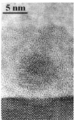
Figure 1 represents a typical bright-field, cross-section TEM共XTEM兲 image taken with the electron beam direction close to the 共110兲-zone axis in strongly underfocused condi-tion of a sample from wafer 1. Under this condicondi-tion, the Ge–ncs show a dark contrast on a gray background. Spheri-cal and well-separated Ge–ncs embedded in the SiO2 layer are clearly observed. The average distance of the dots from the Si substrate is measured to be 4.4 nm关Fig. 2共a兲兴 and the average distance between the dots can be directly measured on such XTEM images. The mean size and density of the dots are measured under the same imaging conditions but on plan view specimens. Typical values of size and aerial
den-sity are found to be 4.5 nm and 3⫻1011cm⫺2, respectively, on wafer 1关Fig. 2共b兲兴. Moreover, the crystalline nature of the Ge dots is evidenced in HRTEM images such as the one shown in Fig. 3. In such large dots (⬃7 nm) twinning of the
兵111其 planes is observed while the distance from the dot to
the substrate could be as small as 2 nm. The results are also found to be similar for samples from wafer 2.
The RBS/channeling results elucidate the recovery of Ge from its oxide state during reduction without Ge diffusion
共not shown兲. A strong evidence of charge storage effect in the
crystalline Ge-nanodot layer is demonstrated by the anti-clockwise hysteresis behavior in the high-frequency C – V characteristic for a sample from wafer 1共Fig. 4兲. High posi-tive and negaposi-tive gate voltages cause the C – V curves to shift in the direction of stored negative and positive charges, re-spectively, while no hysteresis appears at 2 V gate voltage FIG. 1. Bright-field image of a cross-section sample from wafer 1, oxidized
at 800 °C for 14 min in O2followed by reduction at 950 °C for 30 s in N2.
Ge–ncs show a dark contrast on the gray background of the SiO2layer.
FIG. 2. Distributions of tunnel injection distance, i.e., the distance between a Ge nanocrystal and the Si substrate共a兲 and size of the Ge–ncs 共b兲, for sample of wafer 1, oxidized at 800 °C for 14 min in O2followed by
reduc-tion at 950 °C for 30 s in N2. The mean values⫾ the standard deviations of
these distributions are (4.4⫾1.4) and (4.5⫾1.8) nm, respectively.
FIG. 3. HRTEM image of a crystalline isolated Ge nanodot.
FIG. 4. High-frequency C – V curves of samples from wafer 1, oxidized at 800 °C for 14 min in O2followed by reduction at 950 °C for 30 s in N2.
High positive and negative gate voltages cause electron and hole injections respectively into the oxide from the substrate. A gate voltage (Vg) sweep from inversion to accumulation and from accumulation to inversion is shown by the arrow to the left and to the right, respectively.
1213
(Vg) sweep. In the former case, charge trapping occurs
through electron and hole injection from the substrate into the oxide. A gradual increase in the flatband voltage shift (⌬VT) with increasing Vgsweep until 22 V is also observed
and⌬VTis measured to be 0.5 V for Vg⫽6 V. No flatband
voltage shift is observed for the reference sample prepared from wafer 3 by oxidizing only at 800 °C for 14 min in O2
ambiance, implying that the memory effect is Ge nanocrys-tals related. A similar flatband voltage shift is also observed for samples from wafer 2.
The self-assembling phenomenon of Ge nanodots in SiO2 can be explained using the Ostwald ripening mechanism,12 which describes the growth of larger particles at the expense of smaller particles. Shklyaev et al.13showed that thin MBE grown Ge layers on a Si substrate covered with a thin SiO2, formed a high density of hemispherical Ge
island with some connected islands. Such a structure could initiate the Ostwald ripening mechanism as it requires diffu-sion of Ge atoms from the peripheral/valley regions of Ge islands towards their respective centers to construct spherical dots for achieving greater volume to surface ratio. In our case, TEM investigations demonstrate that all the islands are connected until the oxidation of the Si capping layer is com-pleted. Thus, the Ge-dot formation takes place after complete oxidation of the Si capping layer but still during the oxida-tion process. An appreciable amount of Ge is oxidized during the Ge-dot formation.5,11For this reason the reduction pro-cess is essential to recover the Ge nanodots from their oxide state. During thermal treatment in a N2 ambiance, the GeO2
clusters are reduced by Si atoms arriving from the SiO2/Si
interface according to the chemical reaction Si⫹GeO2→Ge
⫹SiO2. 14
It is revealed from Fig. 1 that the Ge dots are formed near to their initial positions, which could be due to a smaller Ge diffusion coefficient compared to Si.14 A reduc-tion time longer than the optimized one leads to the forma-tion of bigger Ge–ncs by coalescence of smaller Ge–ncs and a concomitant reduction in the tunneling distance. Thin Ge layer produces small dots and the homogeneity of the dot size is also correlated with the uniformity of the thickness of the Ge layer. The advantage of using MBE for the deposition of the Ge and Si layers is the precision by which very thin
共e.g., 0.7 nm兲 uniform layers can be deposited.
In summary, we have demonstrated a fabrication tech-nique, which is capable of producing a layer of crystalline Ge nanodots in SiO2, based on MBE in conjunction with
optimized RTP. The Si/Ge sandwiched layers were grown by MBE on 4- and 7-nm-thick SiO2 covered p-Si wafers. The
structural investigations were performed by TEM, HRTEM, and RBS/channeling. The average dimension of the Ge–ncs were found to be 4.5 nm with average aerial density of 3
⫻1011 cm⫺2. The average tunneling oxide thickness was
es-timated to be 4.4 nm. Twins were observed in some bigger crystalline dots of ⬃7 nm. Finally, a significant memory ef-fect was manifested by the hysteresis in the high-frequency
C – V measurements for the optimized samples.
This work was a part of the NEON Project and was funded by the EC as GROWTH GRD1-2000-25619 and by the Danish Strategic Material Research Program. The authors acknowledge the help received from P. Bomholt for prepar-ing TEM samples.
1S. Tiwari, F. Rana, H. Hanafi, A. Hartstein, E. F. Crabbe´, and K. Chan,
Appl. Phys. Lett. 68, 1377共1996兲.
2
Y. H. Kwon, C. J. Park, W. C. Lee, D. J. Fu, Y. Shon, T. W. Kang, C. Y. Hong, H. Y. Cho, and K. L. Wang, Appl. Phys. Lett. 80, 2502共2002兲.
3S. Tiwari, F. Rana, K. Chan, L. Shi, and H. Hanafi, Appl. Phys. Lett. 69,
1232共1996兲.
4I. Kim, S. Han, K. Han, J. Lee, and H. Shin, Jpn. J. Appl. Phys., Part 1 40,
447共2001兲.
5W. K. Choi, W. K. Chim, C. L. Heng, L. W. Teo, V. Ho, V. Ng, D. A.
Antoniadis, and E. A. Fitzgerald, Appl. Phys. Lett. 80, 2014共2002兲.
6C. Bonafos, B. Garrido, M. Lopez, A. Perez-Rodriguez, J. R. Morante, Y.
Kihn, G. Ben Assayag, and A. Claverie, Appl. Phys. Lett. 76, 3962共2000兲.
7
J. von Borany, R. Gro¨tzschel, K. H. Heinig, A. Markwitz, W. Matz, B. Schmidt, and W. Skorupa, Appl. Phys. Lett. 71, 3215共1997兲.
8W. K. Choi, W. K. Chim, C. L. Heng, L. W. Teo, V. Ho, V. Ng, D. A.
Antoniadis, and E. A. Fitzgerald, Appl. Phys. Lett. 80, 2014共2002兲.
9
Y. Kanemitsu, H. Uto, Y. Masumoto, and Y. Maeda, Appl. Phys. Lett. 61, 2187共1992兲.
10S. Yu. Shirayaev, J. Lundsgaard Hansen, P. Kringhøj, and A. Nylandsted
Larsen, Appl. Phys. Lett. 67, 2287共1995兲.
11W. K. Choi, Y. W. Ho, S. P. Ng, and V. Ng, J. Appl. Phys. 89, 2168共2001兲. 12
W. Ostwald, Z. Phys. Chem.共Leipzig兲 34, 495 共1900兲.
13A. A. Shklyaev, M. Shibata, and M. Ichikawa, Phys. Rev. B 62, 1540 共2000兲.
14Y. Maeda, Phys. Rev. B 51, 1658共1995兲.