HAL Id: hal-02269025
https://hal.univ-grenoble-alpes.fr/hal-02269025
Submitted on 18 Dec 2020HAL is a multi-disciplinary open access archive for the deposit and dissemination of sci-entific research documents, whether they are pub-lished or not. The documents may come from teaching and research institutions in France or abroad, or from public or private research centers.
L’archive ouverte pluridisciplinaire HAL, est destinée au dépôt et à la diffusion de documents scientifiques de niveau recherche, publiés ou non, émanant des établissements d’enseignement et de recherche français ou étrangers, des laboratoires publics ou privés.
Role of Ga Surface Diffusion in the Elongation
Mechanism and Optical Properties of Catalyst-Free
GaN Nanowires Grown by Molecular Beam Epitaxy
Marion Gruart, Gwenolé Jacopin, Bruno Daudin
To cite this version:
Marion Gruart, Gwenolé Jacopin, Bruno Daudin. Role of Ga Surface Diffusion in the Elongation Mech-anism and Optical Properties of Catalyst-Free GaN Nanowires Grown by Molecular Beam Epitaxy. Nano Letters, American Chemical Society, 2019, 19 (7), pp.4250-4256. �10.1021/acs.nanolett.9b00023�. �hal-02269025�
The role of Ga surface diffusion in the elongation
mechanism and optical properties of catalyst-free
GaN nanowires grown by molecular beam epitaxy
Marion Gruart1, Gwénolé Jacopin2 and Bruno Daudin1
1Université Grenoble Alpes, CEA, INAC, F-38000 Grenoble
2Institut Néel, Université Grenoble Alpes, CNRS, Grenoble INP, 38000 Grenoble, France.
ABSTRACT: We have shown that both the morphology and elongation mechanism of GaN nanowires homoepitaxially grown by plasma-assisted molecular beam epitaxy (PA-MBE) on a [0001]-oriented GaN nanowire template are strongly affected by the nominal gallium/nitrogen flux ratio as well as by additional Ga flux diffusing from the side walls. Nitrogen-rich growth conditions are found to be associated to a surface energy-driven morphology and reduced Ga diffusion on the (0001) plane. This leads to random nucleation on the (0001) top surface and preferential material accumulation at the periphery. By contrast, gallium-rich growth conditions are characterized by enhanced Ga surface diffusion promoting a kinetically-driven morphology. This regime is governed by a potential barrier which limits diffusion from the top surface towards nanowire side walls, leading to a concave nanowire top surface morphology. Switching from one regime to the other can be achieved using the surfactant effect of an additional In flux. The optical properties are found to be strongly affected by growth mode, with point defect incorporation and stacking fault formation depending on gallium/nitrogen flux ratio.
KEYWORDS: GaN, nanowires, diffusion barrier, plasma-assisted molecular beam epitaxy, cathodoluminescence.
Due to their remarkable structural and optical properties, semiconductor nanowires (NWs) are a subject of current interest. In particular, their large length/diameter and surface/volume ratio are expected to favor elastic strain relaxation in semiconductor NW axial1 or core-shell2
heterostructures consisting of stacked lattice-mismatched materials. This is especially true in the case of the III-nitride family. While III-nitride-based light emitting devices (LEDs) are now firmly established as the current solution for solid state lighting and related applications, limitations related to the high density of extended defects remain. This results from the lack of lattice-adapted substrates and the different lattice parameters of the three binary compounds GaN, InN and AlN. The use of III-nitride nanowires (NWs) has long been identified as a potential solution to address this issue. Indeed, the reduced diameter of the NWs and their large length/diameter aspect ratio favors the elastic relaxation of heterostructures due to their large surface to volume ratio. For GaN/InGaN NW heterostructures, increased wavelength emission requires an increasing InN molar fraction resulting in an increased amount of strain energy. The pioneering work of K. Kishino and coworkers has shown that using NWs allows one to extend emission wavelengths to green and red3–5, opening the path to a new generation of LEDs
potentially emitting across the whole visible spectrum.
Optimization of such potential devices requires a full understanding of nitride NWs growth mode. In focusing on [0001]-oriented GaN NWs grown by plasma-assisted molecular beam epitaxy (PA-MBE), it has been shown that they can spontaneously nucleate on a variety of substrates6–14.This includes lithographically patterned substrates and has led to the formation
of in-plane ordered [0001]-oriented NW arrays grown by selective area growth (SAG)15.
Remarkably, whatever the substrate used, III-nitride NWs can be grown by PA-MBE in absence of any catalyst. By contrast to the case of catalyzed NW growth, following either the vapor-liquid-solid (VLS) or the vapor-solid-solid (VSS) mechanisms, the growth mode of catalyst-free NWs has been relatively poorly studied. More specifically concerning the elongation
mechanism of [0001]-oriented GaN NWs, i.e. the nucleation mechanism of a new layer on their top, is still not clear. In the case of bidimensional layers, the homoepitaxial growth of GaN has been found to occur either in the step-flow mode or being dominated by the formation of hillocks. This transition depends on growth conditions, specifically substrate temperature and Ga/active N flux ratio. These features have been assigned to the effect of the Ehrlich-Schwöbel barrier for the surface diffusion of Ga adatoms16. In this context, the top of a self-nucleated,
catalyst-free GaN NW grown by PA-MBE (typically 50-80 nm wide) can be viewed as a single terrace surrounded by an infinitely high single hexagon-shaped step associated with a barrier limiting the downward diffusion of Ga. In addition, following the model proposed by Debnath et al17, the Ga flux collected on the side walls of GaN NWs and diffusing towards the top is
expected to be similarly affected by a diffusion barrier.
Because of this effect, self-nucleated GaN NWs and GaN NWs grown using the SAG technique offer a unique opportunity to study the impact of surface diffusion barriers on morphology in a system of reduced size consisting of a single terrace. It can also enable the evaluation of the impact of growth conditions on the nucleation of a new layer on top of such terraces. Indeed, it will be demonstrated in this work that the nucleation of such a layer preferably occurs in the periphery. Furthermore, it will be shown that top surface roughness is directly affected by the nucleation mode. While long Ga diffusion lengths result in a smooth and concave top due to the presence of a peripheral downwards diffusion barrier, short diffusion lengths are associated with rough top surfaces resulting in a morphology governed by surface energy.
Results:
The pseudo-templates consisted of ordered arrays of Ga-polar GaN NW ensembles grown by metalorganic chemical vapour deposition on a patterned GaN/sapphire substrate. The mask consisted of SiN which was patterned by e-beam electron lithography to achieve a series of
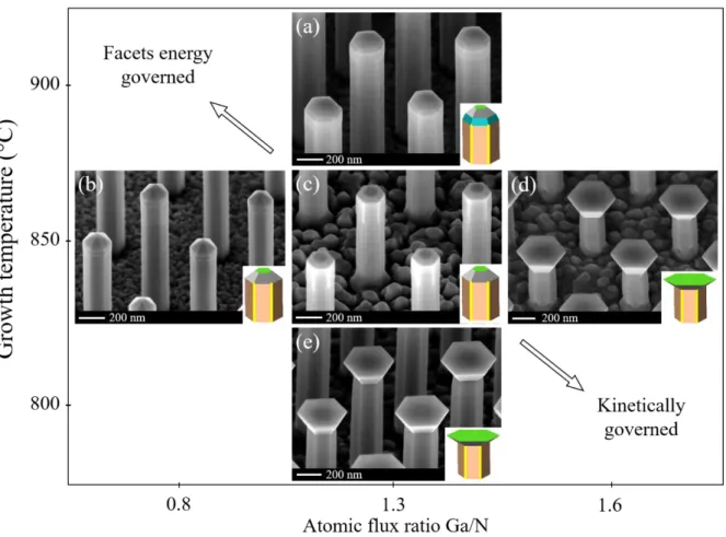
holes with diameter ranging from 30 to 250 nm and pitches comprised between 200 and 800 nm. The diameter of the MOCVD-grown GaN NW templates varied from 120 to 430 nm. Following introduction in the PA-MBE growth chamber and outgassing at 900 °C during 30 minutes, GaN overgrowth was performed for different growth temperatures and impinging Ga/N flux ratio values. Depending on the growth conditions, the thickness of the MBE overgrown section was about 100-200 nm. The impinging nominal Ga/N flux ratio, where N refers to the active N flux, will be denoted Ga/N flux ratio. As shown in Figure 1, the morphology of the MBE overgrown section is homogeneous from wire to wire (see figure S1 in supporting information, further assessing homogeneity at large scale). This morphology can be controlled by changing the Ga/N flux ratio. More precisely, Figure 1b and 1c show the formation of a truncated faceted pyramid, as schematized in the inset. This result is consistent with recent theoretical predictions based on the calculation of surface energies and Wulff construction showing that the equilibrium morphology of Ga-polar crystals should depend on the Ga/N flux ratio18. However, it should be noted that MBE growth is usually performed far
from thermodynamic equilibrium conditions, emphasizing the role of kinetic parameters. Whereas a full pyramidal shape should be theoretically expected for Ga-rich conditions, Figure 1d demonstrates the formation of enlarged nanowires with a flat (0001) top surface. Such a feature is assigned to the lowering of both N and Ga adatoms surface diffusion barriers under very Ga-rich conditions leading to a smooth surface in the case of layers19,20. In the case of
NWs, the enhanced N diffusion on a Ga-saturated (0001) surface is expected to result in enhanced N recombination/desorption and a reduced vertical growth rate19,21, favoring the
formation of a flat (0001) top surface. Additionally, the Ga saturation of the top surface favors nucleation on the side walls and an increase in lateral growth rate leading to NW widening as illustrated in Figure 1d.
This is further supported by results reported in Figure 1a and 1e illustrating the effect of growth temperature for a fixed nominal Ga/N flux ratio value of 1.3. At 800°C (Figure 1e), the formation of flat top surfaces is observed, assigned to a lower desorption rate of Ga and switching of the local growth conditions on top to Ga-rich. By contrast, at 900°C the top morphology is similar to that obtained at 850°, which is assigned to a higher desorption rate of Ga inducing a shift towards more N-rich conditions without affecting the equilibrium shape of the overgrown GaN section. Finally, it appears that depending on growth conditions, the morphology of the top section can be governed either by surface energy or by kinetics.
Figure 1. SEM images of GaN nanowires and associated schematic in the inset showing the
evolution of nanowire top morphology depending on nominal atomic Ga/N flux ratio and growth temperature after a 30 minutes overgrowth. The samples are grown at (a) 900°C with
Ga/N=1.3, (b,c,d) 850°C with Ga/N=0.8, Ga/N=1.3 and Ga/N=1.6 respectively and (e) 800°C with Ga/N=1.3.
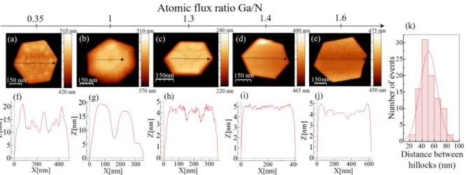
Focusing on the top surface of samples grown at 850 °C, atomic force microscopy (AFM) images and associated height profiles reveal significant differences as a function of the nominal Ga/N flux ratio (see figure 2). At this stage, it should be noted that the effective Ga flux on top of the NW differs from the nominal one due to partial thermal Ga desorption and to the contribution of the Ga flux diffusing along the side walls to the top, which significantly contributes to the vertical growth rate22. It must also be stressed that for a given substrate
temperature, Ga diffusion length depends on the N flux. N-rich conditions are associated with a short Ga diffusion length and very Ga-rich conditions leading to a marked decrease of the adatom surface diffusion barrier on the c-oriented surface19. Accordingly, figure 2a shows a
rough top surface assigned to random nucleation resulting from the short Ga diffusion length on the top c-plane in N-rich conditions. Interestingly, the height profile (figure 2f) further reveals preferential material accumulation at the periphery, consistent with the significant amount of Ga which is expected to diffuse from the side walls at 850°C. However, on the top where Ga diffusion length mostly depends on the Ga/N ratio, a marked roughness is observed with mounds up to about 5 nm high and separated by approximately 50 nm, as attested by the statistics shown in figure 2k. Similarly, surface roughness on a 30 nm length scale was reported by Feenstra et al in the case of a GaN layer grown in N-rich conditions23. Next, for a nominal
Ga/N ratio value of 1 (figure 2b and 2g) a ring of nano-grains, regular in size and spacing, is observed at the periphery, presenting further evidence that nucleation of successive layers is taking place at the frontier between top and vertical side walls. This is confirmed for a higher Ga/N flux ratio of 1.3 (figure 2c and 2h). However in this case, the number of nucleation sites is reduced, giving rise to large terraces which are assigned to a longer Ga diffusion length correlated to Ga-rich conditions. The AFM height profile evidences trenches, about 1 nm deep,
between the terraces. The absence of extra material at the periphery is consistent with the progressive shift from Ga-limited (N-rich) to N-limited (Ga-rich) growth conditions and the subsequent increase of the nucleation probability on top, balancing the role of peripheral nucleation. Further increasing the Ga/N flux ratio finally leads to an atomically flat top surface assigned to a Ga diffusion length equal or longer than half the diameter of the GaN overgrown section. Interestingly in such conditions, as shown in figure 2i, the top surface changes from flat to concave (figure 2j). We tentatively assign this concave morphology to both a preferential nucleation at the periphery and the presence of an energy barrier limiting Ga diffusion toward the lateral walls.
Figure 2. Atomic force microscopy (AFM) (a-e) maps and (f-j) profiles performed on 430 nm
large wires top surfaces with a variation of nominal atomic Ga/N flux ratio. (k) Histogram and normal distribution of distance between hillocks for the sample grown under N-rich conditions, namely Ga/N=0.35. The maximum of the normal distribution is 50 nm.
A further indication of the influence of Ga diffusion length on the NW top morphology and roughness, figure 3 shows the change induced on the top surface of a sample grown in the conditions of figure 2b, i.e. Ga/N=1, when adding an In flux during growth. Indeed, figure 3 puts in evidence a smoothing assigned to a longer Ga diffusion length and a concave morphology similar to samples grown under Ga/N=1.6. It is worth noting that the growth
temperature (850°C) was high enough to prevent any In incorporation in GaN. However, it has been long established that a growing 2D GaN layer can be efficiently smoothed in the presence of an In surface layer acting as a surfactant24. Such an In layer significantly decreases the Ga
adatom surface diffusion barrier resulting in an increased diffusion length, consistent with the results reported in figure 2. This further puts in evidence the impact of Ga diffusion length on top surface roughness. Additionally, it is worth noticing that the In flux smooths the surface but is not changing the morphology as has been observed in Ga-rich conditions in figure 1. Indeed, both wires grown without In (figure 3a) and with In (figure 3d) exhibit a truncated pyramid morphology whatever their diameter, since neither Ga accumulation nor additional nucleation are present on side walls.
Figure 3. SEM images on four different diameter nanowires and AFM maps and profiles on
430 nm large nanowires grown at 850°C and with a nominal flux ratio Ga/N=1 (a,b,c) without indium and (d,e,f) with an additional indium flux.
In order to assess the influence of the growth conditions on the optical properties, cathodoluminescence (CL) experiments have been performed. The acceleration voltage of the electron beam has been set to 3 keV. For such a voltage, 93 % of electron energy is deposited
in the first 50 nm to be sensitive strictly to the PA-MBE overgrown section only (see figure S2 in supporting information). All measurements have been acquired at cryogenic temperature (T ≈ 5 K).
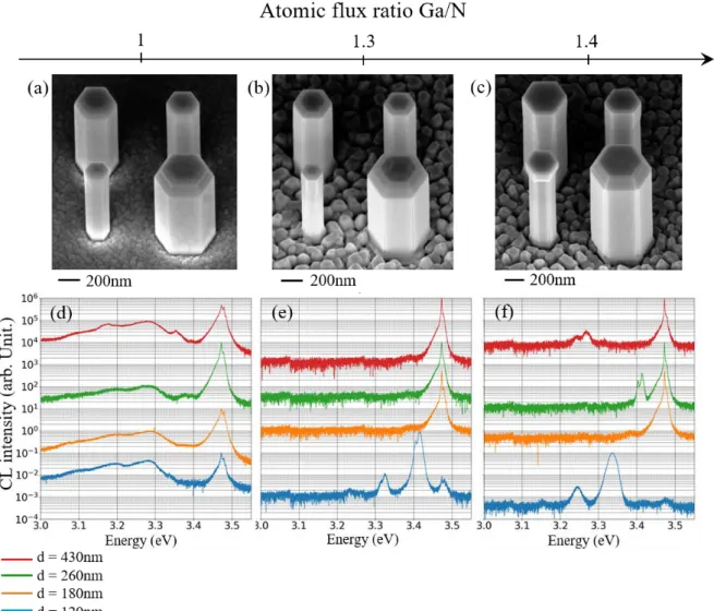
We first studied the role of the Ga/N ratio on the optical properties of the PA-MBE overgrown section. For this purpose, we investigated three samples grown under different nominal Ga/N flux ratio ranging from 1 to 1.4. Since CL spectra may vary from wire to wire within the same sample, we recorded 12 CL spectra of individual wire for each sample (statistics not shown here) to attest to the representativity of the presented spectra. In addition, to probe the influence of the nanowire radius, we inspected wires with 4 different diameters ranging from D = 120 to D = 430 nm. Figure 4(d-f) shows typical spectra for different growth conditions. It should be noted that whatever the Ga flux and nanowire radius, none of the samples exhibited a noticeable yellow luminescence (see Figure S3 in the supporting information).
Figure 4. SEM images and typical CL spectra for the three different samples for different
diameters D = 120 nm (blue), D = 180 nm (orange), D = 260 nm (green) and D =430 nm (red): (a,d) Ga/N = 1, (b,e) Ga/N = 1.3, (c,f) Ga/N = 1.4. All the experiments have been performed at low temperature (T ≈ 5 K).
First, for a nominal Ga/N flux ratio of 1 (figure 4 (a,d)), we observe a strong homogeneity from wire to wire irrespective of their diameter. The near band edge (NBE) emission is characterized by 3 main emission peaks. The predominant emission line may be assigned to a recombination which involves an exciton bound to a neutral Si donor (Si°XA, ≈3.472 eV). This
transition is characterized by a full width at half maximum (FWHM) of 2 meV. In addition, we also observe the signature of free excitons (XA, ≈3.479 eV and XB, ≈3.484 eV). Furthermore,
on some of the wires two additional lines appears at 3.476 eV and 3.468 eV and might be assigned respectively to excited states of Si°XA and an exciton bound to Mg neutral acceptor
Mg°XA. On the 12 probed wires a strong CL contribution appears between 3.0 to 3.3 eV, and
can be ascribed to donor acceptor pair (DAP) transitions.
On the second sample, characterized by nominal Ga/N flux ratio of 1.3, we first notice a strong reduction of the DAP contribution. This indicates that the incorporation of foreign species is reduced under these growth conditions. The near band edge emission is now dominated by a doublet at E≈3.473 eV and E≈3.474eV which may be related to excitons bound to different type of donors (Si°XA and O°XA), characterized by a FWHM of 1.5 meV (limited
by the spectral resolution of the setup). In this sample, one wire (with a diameter of 120 nm) exhibits a strong luminescence around 3.418 eV together with its LO phonon replica at 3.325 eV. This luminescence is associated with a pronounced reduction of the NBE. Hence, this peak could be assigned to the luminescence of basal stacking faults (BSF).
When we further increase the Ga/N flux ratio to 1.4, the probability of BSF creation increases, while the DAP contribution is still absent. The NBE remains dominated by the emission related to Si°XA (≈3.472 eV), FXA (≈3.479 eV) and FXB (≈3.484 eV). In addition, we now observe a
contribution around 3.33 eV on one of the thinner wires, associated with an absence of NBE emission. According to Rieger et al., this may be related to cubic inclusions in the hexagonal GaN25–27. Interestingly, it appears in figure 4c that the thinner wire is slightly enlarged with a
flat top surface while the larger wire exhibits a truncated pyramid morphology. If it is assumed that the Ga diffusion length , along the side walls is only dependent on temperature, it can be easily established (in a cylindrical approximation) that the effective number of Ga and N adatoms on top, nGa and nN respectively, are related to the nominal fluxes and diameter D,
through: nGa nN ~k(T)ФGa ФN (1+tanθ4λ D )
where the nominal ФGa/ФN flux ratio is corrected by a factor k (T) accounting for temperature
dependent desorption from both side walls and top, θ being the incidence angle of Ga and N fluxes with respect to the NW upper surface.
Consistently, the threshold for widening as a function of the Ga flux for a fixed N flux is first observed for the thinner NWs, as put in evidence in figure 4c. Concomitantly, this threshold also corresponds to the threshold for stacking faults formation and/or cubic insertions, associated with 3.3-3.42 eV peaks in CL spectra figure 4e and 4f which are first observed on thinner NWs for increasing Ga flux.
These results have been further confirmed by mapping the CL for two specific energy ranges (3.30 ± 0.04 eV and 3.48 ± 0.04 eV) on a region containing more than 140 wires with nominally the same diameter (D = 170nm) (see Figure S4 in supporting information).
Figure 5. (a) Typical CL spectra for the four different diameters D = 120 nm (blue), D = 180
nm (orange), D = 260 nm (green) and D =430 nm (red) for the sample grown with In surfactant and statistics of the peak energy distribution cumulated for the four different diameters. The width of the histogram is representative of the mean FWHM of the transition. The mean CL spectrum for each sample is overlaid in dashed grey in logscale. (b-c) Monochromatic CL images recorded at 3.48 ± 0.04 eV (b) at 3.30 ± 0.04 eV (c). All the experiments have been performed at low temperature (T ≈ 5 K).
At this stage, it can be concluded that the Ga/N flux ratio has to be increased in order to decrease the defect incorporation (characterized by the intensity of the DAP emission). However, this may lead to the formation of cubic inclusions. The ability of the In surfactant effect to mimic Ga-rich growth conditions while preventing NW widening has been demonstrated above. This beneficial effect is confirmed in figure 5 as concerns optical properties: adding a small amount of In during the growth while keeping a nominal Ga/N flux ratio of 1 indeed results in an excellent optical uniformity from wire to wire (see figure 5 (b-c)) while reducing the intensity ratio between the NBE and the DAP transition by almost two orders of magnitude (see figure 5a). It should be noticed that two additional peaks appear in this sample around 3.36-3.37 eV that may be assigned to the first LO phonon replica of the NBE emission. It then appears that exposing growing NWs to an additional In flux is equivalent to increasing Ga/N flux ratio, emphasizing the role of adatom diffusion on both top roughness and optical properties, but without impacting the nanowire morphology.
Discussion:
It is well established that the effective Ga flux on top of NWs consists of two contributions: the Ga flux directly impinging on the c-oriented top surface and on the Ga flux impinging on the m-oriented side walls and diffusing to the top17. This view has been experimentally
growth rate of 2D layers. It further shows that the effective Ga flux on top is higher than the nominal impinging Ga flux22. These experimental features are consistent with theoretical
calculations of Ga surface diffusion barrier on c-plane19 and m-plane28, respectively. In
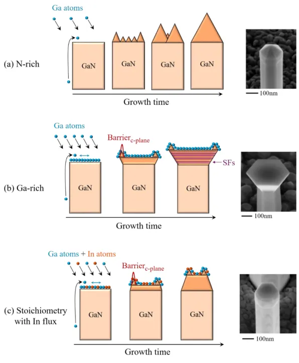
particular, it appears that in N-rich growth conditions the Ga surface diffusion barrier on the c-plane is significantly higher than its counterpart on the m-c-plane. As schematized in figure 6a, it is then expected that Ga diffusing from the side walls towards the NW top will accumulate in the periphery, due to its very short diffusion length on the c-plane, leading to the preferred peripheral nucleation of GaN pyramids. The size increase of such pyramids combined with random GaN nucleation on top leads to their progressive coalescence and eventually to the formation of a fully facetted NW top as illustrated in figure 6a. It should also be noted that AFM maps and profiles were realized on 430 nm large wires allowing a good visibility of hillock repartition, whereas MBE grown self-nucleated nanowires have a diameter inferior to 100 nm. The hillocks on large NWs were found to be separated approximately by 50 nm (figure 2k), which allows the nucleation of one or two nuclei before filling the full monolayer in the case of self-nucleated NWs. This suggests that the elongation of self-nucleated NWs likely obeys a layer-by-layer mechanism, with the nucleation of each successive layer preferentially occurring on the edge.
By contrast, in Ga-rich conditions associated with a long diffusion length of Ga adatom on the c-plane, the presence of an energy barrier preventing Ga adatoms to diffuse from c-plane NW tops towards m-plane sides results in an increased probability of Ga presence at the periphery and preferred peripheral nucleation as schematized in figure 6b. It is worth noting that such a peripheral GaN nucleation mechanism is drastically different in nature from the one illustrated in figure 6a. In the long diffusion length regime, the NW top is first flat, eventually evolving towards a concave shape. We suggest that the reason for the formation of such a concave top is similar to the one giving rise to the formation of inverted wedding cake
morphology of wire structures far larger in size, with a top surface larger than the adatom diffusion length29.Accordingly, the lower limit of Ga adatom diffusion length should be of the
order of half the NW diameter, namely about 220 nm. In such Ga-rich conditions on top, accumulation of Ga is expected on the side walls leading to an increased nucleation probability and NW widening associated with stacking faults formation21,30, accounting for the final
morphology observed (see figure 6b).
The role of In as a surfactant for growth of GaN layers has been experimentally put in evidence by Widmann and coworkers24. It has been demonstrated that the formation of a
continuous In layer on the surface decreased the height of the Ga surface diffusion barrier associated with growth in N-rich conditions, leading to a smoothing of the GaN layer31. As
schematized in figure 6c, exposing GaN NWs grown in nominal stoichiometry conditions to an In flux at a temperature high enough to prevent any In incorporation leads to a smoothing of the surface. The concave morphology of the top NW surface supports the increase of Ga adatom diffusion length associated with the formation of a metallic In surface layer, consistent with the schematics in figure 6b. However, in absence of Ga saturation of the top surface, neither additional nucleation on the side walls nor NW widening are observed, leading to the absence of stacking faults and a marked improvement of optical properties.
Figure 6. Schematics illustrating the elongation mechanism of GaN NWs and associated SEM
images after a 30 minutes growth (a) in N-rich condition, (b) in Ga-rich condition and (c) at stoichiometry with an additional indium flux.
Summary and conclusion:
In summary, we have shown that for the whole set of growth parameters which have been examined the elongation mechanism of Ga-polar GaN NWs is governed by peripheral nucleation. The physical reason accounting for this process is dependent on the details of
growth conditions prevailing on the top surface. In the case of N-rich conditions, Ga accumulation at the periphery is observed, which is related to the significant Ga diffusion from the side walls towards the top, compared to the reduced diffusion length on the c-plane. In such a case, the final morphology of the NW top is surface energy-determined and consists of a facetted pyramid. By contrast, metal-rich conditions lead to an enhancement of the Ga diffusion length associated with a smoothing of the top surface. In that case, peripheral nucleation is a consequence of Ga accumulation assigned to the presence of an energy barrier preventing Ga adatoms from diffusing down from top to NW walls. Optimized optical properties in terms of band edge emission are found for conditions close to stoichiometry combining a flat top surface and an absence of widening/stacking faults. This more generally suggests that fine tuning of metal/N flux ratio is essential to optimize the optical properties of nitride NWs.
AUTHOR INFORMATION
Corresponding Author
*E-mail: marion.gruart@cea.fr
Acknowledgments: The authors acknowledge Y. Curé for MBE growth technical assistance
and Dr. W. Chikhaoui for fruitful discussions. REFERENCES
(1) Glas, F. Phys. Rev. B. 2006, 74 (12), 121302.
(2) Raychaudhuri, S.; Yu, E. T. J. Appl. Phys. 2006, 99 (11), 114308.
(3) Sekiguchi, H.; Kishino, K.; Kikuchi, A. Appl. Phys. Lett. 2010, 96 (23), 231104. (4) Kishino, K.; Nagashima, K.; Yamano, K. Appl. Phys. Express 2013, 6 (1), 012101.
(5) Yanagihara, A.; Ikeda, K.; Kishino, K.; Yamano, K. Electron. Lett. 2015, 51 (11), 852– 854.
(6) Yoshizawa, M.; Kikuchi, A.; Mori, M.; Fujita, N.; Kishino, K. Jpn. J. Appl. Phys. 1997, 36, L459.
(7) Calleja, E.; Ristić, J.; Fernández-Garrido, S.; Cerutti, L.; Sánchez-García, M. A.; Grandal, J.; Trampert, A.; Jahn, U.; Sánchez, G.; Griol, A.; Sánchez, B. Phys. Status Solidi B
2007, 244 (8), 2816–2837.
(8) Stoica, T.; Sutter, E.; Meijers, R. J.; Debnath, R. K.; Calarco, R.; Lüth, H.; Grützmacher, D. Small 2008, 4 (6), 751–754.
(9) Fernández-Garrido, S.; Kong, X.; Gotschke, T.; Calarco, R.; Geelhaar, L.; Trampert, A.; Brandt, O. Nano Lett. 2012, 12 (12), 6119–6125.
(10) Schuster, F.; Furtmayr, F.; Zamani, R.; Magén, C.; Morante, J. R.; Arbiol, J.; Garrido, J. A.; Stutzmann, M. Nano Lett. 2012, 12 (5), 2199–2204.
(11) Nakagawa, S.; Tabata, T.; Honda, Y.; Yamaguchi, M.; Amano, H. Jpn. J. Appl. Phys.
2013, 52 (8S), 08JE07.
(12) Calabrese, G.; Corfdir, P.; Gao, G.; Pfüller, C.; Trampert, A.; Brandt, O.; Geelhaar, L.; Fernández-Garrido, S. Appl. Phys. Lett. 2016, 108 (20), 202101.
(13) May, B. J.; Sarwar, A. T. M. G.; Myers, R. C. Appl. Phys. Lett. 2016, 108 (14), 141103. (14) Calabrese, G.; Pettersen, S. V.; Pfüller, C.; Ramsteiner, M.; Grepstad, J. K.; Brandt, O.; Geelhaar, L.; Fernández-Garrido, S. Nanotechnology 2017, 28 (42), 425602.
(16) Kaufmann, N. A. K.; Lahourcade, L.; Hourahine, B.; Martin, D.; Grandjean, N. J. Cryst.
Growth 2016, 433, 36–42.
(17) Debnath, R. K.; Meijers, R.; Richter, T.; Stoica, T.; Calarco, R.; Lüth, H. Appl. Phys.
Lett. 2007, 90 (12), 123117.
(18) Li, H.; Geelhaar, L.; Riechert, H.; Draxl, C. Phys. Rev. Lett. 2015, 115 (8), 085503. (19) Zywietz, T.; Neugebauer, J.; Scheffler, M. Appl. Phys. Lett. 1998, 73 (4), 487–489. (20) Mula, G.; Adelmann, C.; Moehl, S.; Oullier, J.; Daudin, B. Phys. Rev. B 2001, 64 (19), 195406.
(21) Zhang, X.; Haas, B.; Rouvière, J.-L.; Robin, E.; Daudin, B. Nanotechnology 2016, 27 (45), 455603.
(22) Songmuang, R.; Ben, T.; Daudin, B.; González, D.; Monroy, E. Nanotechnology 2010, 21 (29), 295605.
(23) Feenstra, R. M.; Chen, H.; Ramachandran, V.; Lee, C. D.; Smith, A. R.; Northrup, J. E.; Zywietz, T.; Neugebauer, J.; Greve, D. W. Surf. Rev. Lett. 2000, 7, 601.
(24) Widmann, F.; Daudin, B.; Feuillet, G.; Pelekanos, N.; Rouvière, J. L. Appl. Phys. Lett.
1998, 73 (18), 2642–2644.
(25) Rieger, W.; Dimitrov, R.; Brunner, D.; Rohrer, E.; Ambacher, O.; Stutzmann, M. Phys.
Rev. B 1996, 54 (24), 17596–17602.
(26) Tischer, I.; Feneberg, M.; Schirra, M.; Yacoub, H.; Sauer, R.; Thonke, K.; Wunderer, T.; Scholz, F.; Dieterle, L.; Müller, E.; Gerthsen, D. Phys. Rev. B 2011, 83 (3), 035314.
(27) Jacopin, G.; Rigutti, L.; Largeau, L.; Fortuna, F.; Furtmayr, F.; Julien, F. H.; Eickhoff, M.; Tchernycheva, M. J. Appl. Phys. 2011, 110 (6), 064313.
(28) Lymperakis, L.; Neugebauer, J. Phys. Rev. B 2009, 79 (24), 241308.
(29) Yin, X.; Geng, D.; Wang, X. Angew. Chem. Int. Ed. 2016, 55 (6), 2217–2221.
(30) Lähnemann, J.; Jahn, U.; Brandt, O.; Flissikowski, T.; Dogan, P.; Grahn, H. T. J. Phys.
Appl. Phys. 2014, 47 (42), 423001.