Publisher’s version / Version de l'éditeur:
Journal of Vacuum Science and Technology A, 22, 3, pp. 943-947, 2004
READ THESE TERMS AND CONDITIONS CAREFULLY BEFORE USING THIS WEBSITE. https://nrc-publications.canada.ca/eng/copyright
Vous avez des questions? Nous pouvons vous aider. Pour communiquer directement avec un auteur, consultez la première page de la revue dans laquelle son article a été publié afin de trouver ses coordonnées. Si vous n’arrivez pas à les repérer, communiquez avec nous à [email protected].
Questions? Contact the NRC Publications Archive team at
[email protected]. If you wish to email the authors directly, please see the first page of the publication for their contact information.
NRC Publications Archive
Archives des publications du CNRC
This publication could be one of several versions: author’s original, accepted manuscript or the publisher’s version. / La version de cette publication peut être l’une des suivantes : la version prépublication de l’auteur, la version acceptée du manuscrit ou la version de l’éditeur.
For the publisher’s version, please access the DOI link below./ Pour consulter la version de l’éditeur, utilisez le lien DOI ci-dessous.
https://doi.org/10.1116/1.1676345
Access and use of this website and the material on it are subject to the Terms and Conditions set forth at
Raman and transmission electron microscopy study of disordered
silicon grown by molecular beam epitaxy
Tay, L.; Lockwood, D. J.; Baribeau, J. -M.; Wu, X.; Sproule, G. I.
https://publications-cnrc.canada.ca/fra/droits
L’accès à ce site Web et l’utilisation de son contenu sont assujettis aux conditions présentées dans le site LISEZ CES CONDITIONS ATTENTIVEMENT AVANT D’UTILISER CE SITE WEB.
NRC Publications Record / Notice d'Archives des publications de CNRC:
https://nrc-publications.canada.ca/eng/view/object/?id=f2d5549f-6c55-4f41-a716-713f9f6e44e0 https://publications-cnrc.canada.ca/fra/voir/objet/?id=f2d5549f-6c55-4f41-a716-713f9f6e44e0grown by molecular beam epitaxy
L. Tay,a)D. J. Lockwood, J.-M. Baribeau, X. Wu, and G. I. Sproule
Institute for Microstructural Sciences, National Research Council Canada, Ottawa K1A 0R6, Canada
~Received 12 September 2003; accepted 20 January 2004; published 18 May 2004!
Silicon films were deposited by molecular beam epitaxy onto crystalline silicon (c-Si) and native oxide on c-Si ~001! substrates at temperatures ranging from 98 to 572 °C. Raman spectroscopy of these films showed that both the short-range disorder and intermediate-range disorder decreases as the deposition temperature increases. The onset of a phase transition in the amorphous Si films can be effectively identified by the appearance of the polycrystalline and crystalline Si Raman bands, which allowed quantification of the crystalline volume fractions present. Both the transmission electron microscopy and Raman results confirmed that films grown on the amorphous substrates at temperatures less than 414 °C are entirely amorphous, but exhibit c-Si features at higher temperatures. Films grown on c-Si substrates exhibit a characteristic limiting thickness for epitaxy and the transformation of the resulting upper amorphous layer into crystalline form takes place at a much lower temperature ~;290 °C! than for the amorphous substrates. © 2004 American Vacuum
Society. @DOI: 10.1116/1.1676345#
I. INTRODUCTION
Silicon ~Si! is the key material in the semiconductor in-dustry. There have been many studies devoted to the thin film deposition of various phases of Si by techniques such as sputtering,1chemical vapor deposition ~CVD!,2and molecu-lar beam epitaxy ~MBE!.3The MBE technique, in particular, is performed in ultrahigh vacuum conditions and offers su-perior control over growth parameters such as temperature and growth rate. Thus, MBE is an interesting alternative to conventional techniques for the synthesis of a noncrystalline Si possessing fewer impurities and improved physical prop-erties. The structural properties of low-temperature high-vacuum deposited Si have, until recently, not been the sub-ject of much investigation. In particular, the degree of disorder in such Si films and its dependence on the process-ing temperature or nature of the substrate have not been fully examined. Earlier studies4 –6 showed that the epitaxial growth of Si on a crystalline Si (c-Si) substrate at a given temperature is characterized by a limiting thickness (hepi) beyond which the growth becomes amorphous. The struc-tural evolution that leads to the epitaxy breakdown has not been studied in great detail and how the properties of those films compare to those of Si films deposited on noncrystal-line substrates has also received little attention.
Raman spectroscopy is a nondestructive characterization technique sensitive to short and long-range atomic order. There have been a number of studies1,8that have employed Raman scattering to characterize the phase transition of CVD grown silicon. It is a convenient method to study silicon phase transitions in amorphous silicon (a-Si),7 polycrystal-line silicon ~poly-Si!,8,9 and c-Si materials.10 Despite its popularity, there have been few reports11of the use of Raman scattering spectroscopy to investigate the levels of disorder
and the phase transitions in low-temperature MBE-grown Si films. Here, we present a comprehensive Raman study of MBE-grown silicon films deposited on both crystalline and amorphous substrates and we compare the degree of film disorder as a function of the deposition temperature and the nature of the substrate. We show that there is a good agree-ment between the results obtained from Raman spectroscopy, secondary ion mass spectrometry ~SIMS!, and transmission electron microscopy ~TEM! imaging.
II. EXPERIMENT
A number of samples were prepared by depositing Si on 100 mm Si ~001! wafers in a VG Semicon V80 MBE system at a fixed growth rate of 0.2 nm/s. For the films grown on
c-Si substrates, the Si wafers were treated in a 5% HF
solu-tion to remove the native oxide. The treatment left the wafer surface passivated with hydrogen, which was desorbed at 600 °C in the ultrahigh vacuum before Si deposition. A series of Si films were also deposited directly on Si ~001! wafers that had received an UV-ozone treatment to reduce hydrocar-bon surface contamination, but no HF treatment to remove the surface native oxide (SiO2/c-Si). Films were deposited in the temperature range from 98 to 572 °C and were typi-cally 350 nm thick.
Raman spectroscopy of each silicon film was performed in an ambient atmosphere of helium at room temperature ~295 K!. Samples were excited with 200 mW of 457.9 nm light from an Ar ion laser. The samples were investigated with a pseudo-backscattering geometry.12The scattered light was dispersed by a Spex 14018 double monochromator at a spectral resolution of 7.8 cm21 and detected with a cooled RCA C31034A photomultiplier tube. The incident light was polarized in the scattering plane and the scattered light was recorded without polarization analysis. In order to obtain the peak intensity, peak width, and integrated area of the various Si-related bands in the measured Raman spectra, a spectral a!Author to whom correspondence should be addressed; electronic mail:
curve fitting was performed using a combined Gaussian– Lorentzian function. The structural properties of the Si thin films grown on both c-Si and SiO2/c-Si substrates were also characterized by cross-sectional TEM to assess their micro-structure and SIMS to probe their impurity incorporation. The TEM samples were examined with a Philips EM430T operating at 250 kV.
Due to the difference in the optical properties of a-Si, poly-Si, and c-Si, the Raman penetration depth for the 457.9 nm radiation varies for different types of films. The Raman penetration depth7 is ;19.2 nm for a-Si,7 ;321.6 nm for
c-Si,12and somewhere in between for poly-Si. Referring to
the film thicknesses shown in Table I, we are confident in concluding that there is very little, if any, Raman contribu-tion from the c-Si substrate.
III. RESULTS AND DISCUSSION
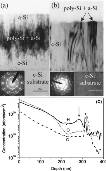
Figures 1~a! and 1~b! show TEM cross-sectional images of a Si film grown at 335 °C on a c-Si substrate and at 572 °C on a SiO2/c-Si substrate, respectively. The concen-tric speckle-like halo rings in both selected area diffraction patterns suggest the presence of both a-Si and poly-Si. The film growth in Fig. 1~a! begins with ;75 nm of perfect crys-talline growth followed by a breakdown of epitaxy charac-terized by the columnar defect structure along the @001# growth direction. This structure is very similar to that found for other MBE films deposited onto a crystalline substrate at low temperature.4This type of growth evolution is, however, different from that for CVD or sputter deposited Si films, which tend to begin their phase transition through the ran-dom formation of pockets of c-Si grains within an a-Si network.13,14Abundant twinning structures ~planar defects! appear in the $111% planes at the interface where the epitaxial breakdown is observed. Such a twinning structure is com-monly observed at the transitional state and acts as the strain relieving mechanism within the crystalline lattice network. On SiO2/c-Si substrates, however, a polycrystalline struc-ture with no definite depth dependence is observed. Dark striations in image ~b! are mostly poly-Si with some a-Si embedded in the poly-Si. They appear to possess a columnar character rather than the stacking fault nature seen in image ~a!. The SIMS profile @see Fig. 1~c!# obtained from the same sample as in Fig. 1~a! shows a peak in the hydrogen
concen-tration at the depth ~denoted by the arrow! where the defects are first observed. This is consistent with H atoms segregat-ing to the surface in the crystalline phase and besegregat-ing incorpo-rated at the transition region. The oxygen and carbon incor-poration remained low until the film crystallinity had strongly deteriorated.
The Raman spectrum of an a-Si epitaxial layer grown at 177 °C on a c-Si substrate is presented in Fig. 2. It is a characteristic a-Si Raman spectrum typified by the strong transverse optical ~TO! and broad transverse acoustic ~TA! phonon bands located at 475.8 and ;150 cm21, respectively. Less obvious longitudinal acoustic ~LA! modes at 299.3 and 400.6 cm21are visible, as shown by the deconvoluted ~fitted! dashed traces in Fig. 2.
Figure 3 shows the Raman spectrum of the Si film de-picted in Fig. 1~a!, with the c-Si spectrum subtracted from it. The Raman spectrum still exhibits a noticeable TA band at 150 cm21. A much narrower band with a rather obvious TABLEI. Summary of the growth temperature, substrate, film thickness and
crystalline volume fractions, Xcfor the films that exhibit the a-Si, poly-Si,
and c-Si Raman signatures. Growth temp. ~°C! Substrate Film thickness ~nm! Xc 295 c-Si 390 0.44 335 c-Si 316 0.88 374 c-Si 367 0.98 335 SiO2/c-Si 370 0.009 414 SiO2/c-Si 260 0.08 493 SiO2/c-Si 400 0.97 572 SiO2/c-Si 410 0.98
FIG. 1. Cross-sectional TEM images and their corresponding selected area diffraction patterns ~insets! of a Si film grown on ~a! a c-Si substrate at 335 °C and ~b! a SiO2/c-Si substrate at 572 °C. The scale bar length is 100 nm. Part ~c! is the hydrogen ~solid line!, oxygen ~dotted line!, and carbon ~dashed line! secondary ion mass spectrometry profile of the Si film depicted in Fig. 1~a!.
944 Tayet al.: Raman and TEM study of disordered silicon grown by MBE 944
shoulder now replaces the broad TO band seen in the a-Si spectrum ~see Fig. 2!. The shoulder structure is a unique indicator of the presence of poly-Si or microcrystalline Si.8 Its asymmetric band shape differs markedly from the c-Si symmetric band at 520 cm21. The deconvoluted TO band comprises the a-Si related band at 481.2 cm21 and the poly-Si related bands at 505.5 and 517.3 cm21~see the inset to Fig. 3!. Depending on the amount of microcrystallinity present in the sample, the two higher frequency bands can vary in intensity. Correlating the Raman spectra in Fig. 3 with the TEM and diffraction results in Fig. 1~a!, it is clear that this film is in a transitional stage at which all three phases of silicon (a-Si, poly-Si and c-Si) coexist. Therefore, the presence of crystalline ~520 cm21! and microcrystalline Si ~505, 517 cm21! bands in the Raman spectra offers an alternative way ~in addition to TEM or x-ray diffraction! to characterize the onset of the phase transition in the MBE deposited Si films grown at various temperatures.
The integrated intensity of the crystalline components, Ic,
normalized to the total scattering intensity in the TO band ~including the a-Si component, Ia, near 480 cm21!is often
used to determine the Si crystalline volume fraction present in the Raman sampled volume.8,15 The crystalline volume fraction evaluated by the formula,15
Xc5Ic/(Ic1yIa),
where y50.28,16 is summarized in Table I. The weighting factor y is the ratio of the integrated Raman cross section for
c-Si to a-Si at the excitation wavelength of 457.9 nm.16
Again, we stress the importance of the difference in the op-tical absorptions of the a-Si and c-Si at 457.9 nm, which is taken into account by the correction factor y in the Xc
ex-pression. It is important to point out that the Xcvalues listed
in Table I are computed strictly for the volume of the film sampled by the Raman beam. For a Si film deposited on a
c-Si substrate, the presence of poly-Si is first observed at
growth temperatures higher than 295 °C. Although there is a thin crystalline epilayer ~due to the limiting thickness issue! present in the samples grown below 295 °C, it is buried un-der a thick layer of a-Si and is not accessible with the 457.9 nm radiation used in the Raman sampling. As the growth temperature increases, the crystalline volume fraction in-creases from 0.44 ~at 295 °C! to 0.98 ~at 374 °C!. The films grown on c-Si at the next temperature of 414 °C or higher produced an entirely c-Si-like Raman signature. Poly-Si Ra-man features were first observed at a higher temperature ~335 °C! for films grown on SiO2/c-Si ~see Table I!. It is interesting to point out that high crystalline volume fractions could be observed in Si films even though they were grown on noncrystalline substrates. This suggests a high degree of crystallinity is achievable on noncrystalline substrates pro-vided that the deposition temperature is high enough.
At low temperature, Si growth on c-Si substrates is ini-tially epitaxial up to a critical thickness beyond which the crystalline growth gives way to amorphous growth. The TEM images in Fig. 1~a! show the evolution of the Si film grown at 335 °C on a c-Si substrate. The growth is epitaxial over the first ;75 nm deposited above the c-Si substrate; it evolves into a poly-Si intermediate layer in the next 200 nm and then finally into a 50-nm-thick layer a-Si near the sur-face. However, films deposited on native oxide SiO2/c-Si have no crystalline template to conform to and grow directly in an amorphous phase and the transition from a-Si to poly-Si occurs at a much higher temperature. Raman spectra of films grown on amorphous substrates suggest the poly-Si phase does not appear below ;500 °C. The growth of poly-Si phases on amorphous substrates had a columnar form and was embedded within an a-Si matrix.
The inelastically scattered light signals arise from the lat-tice vibrations in solids. The various bands observed in the Raman spectrum thus reflect the vibrational density of states of either the optical or acoustic phonons in the solid struc-ture. The TO-like phonon is due to vibrations associated with bonding between nearest neighbor atoms. It is well estab-lished that an increase of the linewidth, G ~defined as the full width at half maximum!, and a decrease of the peak fre-quency, vTO, of the TO band are related to the
root-mean-FIG. 2. Raman spectrum of an a-Si sample ~solid trace! grown at 177 °C on a c-Si substrate. The deconvoluted TO and LA bands are represented by the dashed Gaussian–Lorentzian curves.
FIG. 3. Raman spectrum of a Si film ~solid trace! grown at 335 °C on a c-Si substrate. Dashed curves represents the partially deconvoluted Raman spec-tra. Curve resolved TO bands are shown in the inset.
square bond-angle distortion ~short-range disorder! in a dis-ordered Si network.17,18The peak broadening is due to the random distribution of the internal strain.18The relationship between G and bond-angle distortion ~from the c-Si value of 109.5°! Duhas been established by Beeman, Tsu, and Thorpe who found that G51516Du.17Figure 4 shows a clear trend of decreasing G and hence Duas the deposition temperature increases. At the lowest growth temperature ~98 °C! on the amorphous substrate, the G value of 71.8 cm21corresponds to a bond-angle distortion of 9.47°. For a-Si films grown on a c-Si substrate, the experimentally observed G values ranged from 72.8 to 61.0 cm21 implying bond distortion angles in the range of 9.63° to 7.67° for films grown in the temperature range of 177 to 374 °C. Beeman and co-workers17 reported a Du ranging from 7.7° to 10.5° for MBE films grown at 33 °C and annealed up to 600 °C. The respective Du values are in good agreement. The slightly higher Du found by Beeman and co-workers is due to the lower deposition temperature of 33 °C. The decrease in Du
implies that the deposited film becomes more ordered with increasing deposition temperature. However, G for the c-Si substrate case ~solid square, Fig. 4! showed a slight increase at the highest growth temperature where poly-Si or a-Si is formed ~374 °C!. A similar effect has been observed in glow discharge and sputter deposited Si films.19This is due to the contributions from two opposing factors. As the temperature increases, the higher mobility of Si atoms improves the net-work relaxation. On the other hand, hydrogen dissociation at higher temperature removes its strain relieving effect from the Si network.19 Results from SIMS confirmed a much lower level of H content in the film grown at 374 °C or above.20
As the growth temperature increases, an increasing trend from 477.3 cm21at 98 °C to 490.6 cm21at 493 °C forv
TO also indicates diminishing disorder in the deposited films. At the highest deposition temperature of 572 °C, we found that the film grown on SiO2/c-Si shows a relatively lowervTO value. This change corresponds to the onset of the formation of poly-Si and an abrupt change in the short-range order
within the epilayer. The results overall agree well with the cross-sectional TEM study.
In contrast to the TO mode, the TA mode is associated with vibrations of disordered structures that extend beyond the immediate neighboring atoms, of the order of 4 –6 Å or greater.21 Thus the TA peak intensity in Raman spectra is a good indication of the intermediate range disorder. To ex-clude the possibility of contributions from sample to sample intensity variations due to changes in optical absorption, the intensity ratio of the TA peak to TO peak, ITA/ITO, is taken as the measure of intermediate range disorder for the a-Si network. Hence, a decrease in the intermediate-range order is manifested in an increase of the intensity ratio of the TA and TO bands. This trend is most evident in films grown on SiO2/c-Si. As the growth temperature of the a-Si film in-creases, the ITA/ITOratio shows a general decreasing trend from 0.67 at 98 °C to 0.22 at 572 °C, indicating an increase of intermediate-range order. In the case of c-Si substrates, we observed a sudden increase in the band ratio at 295 °C. This, again, shows a connection to the onset of a phase tran-sition from a-Si into poly-Si and hence an abrupt change in the intermediate-range disorder.
IV. CONCLUSION
We have presented detailed Raman characterization re-sults for MBE-grown Si films deposited on c-Si ~001! and SiO2/c-Si ~001! at various growth temperatures. The ob-served decrease in the TO phonon bandwidth and increase in the peak frequency as the growth temperature increases in-dicate an increased short-range order within the film net-work. In addition, the decrease in the TA-to-TO band inten-sity ratio indicates an increase in the intermediate-range order as the film growth temperature increases. We have also shown that the onset of the phase transition from a-Si into poly-Si and c-Si films can be easily characterized by the appearance of the related Raman bands near 505 and 517 and 520 cm21, respectively. We have determined the volume fraction, Xc, of the crystalline phase in the films deposited
onto the different substrates and it rises steeply at first with increasing growth temperature. Finally, we have demon-strated that Raman spectroscopy is a convenient and effec-tive way to study the degree of disorder and to identify the phase transition in MBE-grown silicon films.
1K. Xu, S. I. Shah, and D. Guerin, J. Vac. Sci. Technol. A 19, 1078 ~2001!. 2D. Han, G. Yue, J. D. Lorentzen, J. Lin, H. Habuchi, and Q. Wang, J.
Appl. Phys. 87, 1882 ~2000!.
3D. J. Eaglesham, J. Appl. Phys. 77, 3597 ~1995!.
4D. J. Eaglesham, H. J. Gossmann, and M. Cerullo, Phys. Rev. Lett. 65, 1227 ~1990!.
5D. J. Eaglesham, J. Appl. Phys. 62, 2566 ~1993!.
6J. Thiesen, H. M. Branz, and R. S. Crandall, Appl. Phys. Lett. 77, 3589 ~2000!.
7P. X. Zhang, I. V. Mitchell, B. Y. Tong, P. J. Schultz, and D. J. Lockwood, Phys. Rev. B 50, 17080 ~1994!.
8M. Zhu, X. Guo, G. Chen, H. Han, M. He, and K. Sun, Thin Solid Films
360, 205 ~2000!.
9Z. Iqbal, S. Veprek, A. P. Webb, and P. Capezzuto, Solid State Commun.
37, 993 ~1981!.
10P. Y. Yu and M. Cardona, Fundamentals of Semiconductors, 2nd ed. ~Springer, Berlin, 1999!.
FIG. 4. Linewidth, G, of the TO band is plotted as a function of the film growth temperature for the two different substrates.
946 Tayet al.: Raman and TEM study of disordered silicon grown by MBE 946
11D. J. Lockwood, J.-M. Baribeau, M. Noel, J. C. Zwinkels, B. J. Fogal, and S. K. O’Leary, Mater. Res. Soc. Symp. Proc. 609, A5.1.1 ~2000!; D. J. Lockwood, J.-M. Baribeau, M. Noel, J. C. Zwinkels, B. J. Fogal, F. Ora-punt, and S. K. O’Leary, ibid. 715, A19.1.1 ~2002!.
12D. J. Lockwood, M. W. C. Dharma-Wardana, J. M. Baribeau, and D. C. Houghton, Phys. Rev. B 35, 2243 ~1987!.
13A. Lambertz, B. S. Richards, A. B. Sproul, T. Puzzer, and M. Gross, Proceedings of the Second World Conference and Exhibition on Photo-voltaic Solar Energy Conversion, Vienna, Austria, 6–10 July ~1998!, VB1.22.
14T. Sasaki, S. Fujikake, K. Tabuchi, T. Yoshida, T. Hama, H. Sakai, and Y. Ichikawa, J. Non-Cryst. Solids 266–269, 171 ~2000!.
15R. Tsu, J. Gonzales-Hernandez, S. S. Chu, S. C. Lee, and K. Tanaka, Appl. Phys. Lett. 40, 534 ~1982!.
16From Ref. 15, y5(I
c/ac)/(Ia/aa) whereais the absorption coefficient
for crystalline and amorphous Si at the excitation wavelength of 457.9 nm. Using ac53.583104/cm21 obtained from Ref. 12 and aa56.0
3105cm21 obtained from Ref. 7, and Ic/Ia54.70 determined
experi-mentally, y is calculated to be 0.28 for 457.9 nm excitation. 17D. Beeman, R. Tsu, and M. F. Thorpe, Phys. Rev. B 32, 874 ~1985!. 18R. Tsu, J. Gonzalez-Hernandez, and F. H. Pollak, Solid State Commun.
54, 447 ~1985!.
19G. Morell, R. S. Katiyar, S. Z. Weisz, H. Jia, J. Shinar, and I. Balberg, J. Appl. Phys. 78, 5120 ~1995!.
20J. M. Baribeau, X. Wu, D. J. Lockwood, L. Tay, and G. I. Sproule, J. Vac. Sci. Technol. ~in press!.
21A. P. Sokolov, A. P. Shebanin, O. A. Golikova, and M. M. Mezdrogina, J. Phys. Condens. Matter 3, 9887 ~1991!.