HAL Id: hal-01715333
https://hal.archives-ouvertes.fr/hal-01715333
Submitted on 22 Feb 2018
HAL is a multi-disciplinary open access
archive for the deposit and dissemination of
sci-entific research documents, whether they are
pub-lished or not. The documents may come from
teaching and research institutions in France or
abroad, or from public or private research centers.
L’archive ouverte pluridisciplinaire HAL, est
destinée au dépôt et à la diffusion de documents
scientifiques de niveau recherche, publiés ou non,
émanant des établissements d’enseignement et de
recherche français ou étrangers, des laboratoires
publics ou privés.
In-situ NC-AFM measurements of high quality
AlN(0001) layers grown at low growth rate on
4H-SiC(0001) and Si(111) substrates using ammonia
molecular beam epitaxy
Florian Chaumeton, Sebastien Gauthier, David Martrou
To cite this version:
Florian Chaumeton, Sebastien Gauthier, David Martrou. In-situ NC-AFM measurements of high
quality AlN(0001) layers grown at low growth rate on 4H-SiC(0001) and Si(111) substrates using
ammonia molecular beam epitaxy. AIP Advances, American Institute of Physics- AIP Publishing
LLC, 2015, 5 (6), pp.67108-1 - 67108-10. �10.1063/1.4922193�. �hal-01715333�
rate on 4H-SiC(0001) and Si(111) substrates using ammonia molecular beam epitaxy
Florian Chaumeton, Sébastien Gauthier, and David MartrouCitation: AIP Advances 5, 067108 (2015); doi: 10.1063/1.4922193 View online: https://doi.org/10.1063/1.4922193
View Table of Contents: http://aip.scitation.org/toc/adv/5/6
Published by the American Institute of Physics
Articles you may be interested in
The origin of stress reduction by low-temperature AlN interlayers
Applied Physics Letters 81, 2722 (2002); 10.1063/1.1512331
Control of GaN surface morphologies using plasma-assisted molecular beam epitaxy
Journal of Applied Physics 88, 1855 (2000); 10.1063/1.1305830
Role of threading dislocation structure on the x-ray diffraction peak widths in epitaxial GaN films
Applied Physics Letters 68, 643 (1996); 10.1063/1.116495
Wafer-level MOCVD growth of AlGaN/GaN-on-Si HEMT structures with ultra-high room temperature 2DEG mobility
AIP Advances 6, 115016 (2016); 10.1063/1.4967816
Two-dimensional electron gases induced by spontaneous and piezoelectric polarization charges in N- and Ga-face AlGaN/GaN heterostructures
Journal of Applied Physics 85, 3222 (1999); 10.1063/1.369664
GaN, AlN, and InN: A review
Journal of Vacuum Science & Technology B: Microelectronics and Nanometer Structures Processing, Measurement, and Phenomena 10, 1237 (1992); 10.1116/1.585897
AIP ADVANCES 5, 067108 (2015)
In-situ NC-AFM measurements of high quality AlN(0001)
layers grown at low growth rate on 4H-SiC(0001) and Si(111)
substrates using ammonia molecular beam epitaxy
Florian Chaumeton,aSébastien Gauthier,band David Martrouc
CNRS/ CEMES / GNS, 29 rue Jeanne Marvig, 30155 Toulouse, France
(Received 14 January 2015; accepted 22 May 2015; published online 2 June 2015)
Nitride wide-band-gap semiconductors are used to make high power electronic devices or efficient light sources. The performance of GaN-based devices is directly linked to the initial AlN buffer layer. During the last twenty years of research on nitride growth, only few information on the AlN surface quality have been obtained, mainly by ex-situ characterization techniques. Thanks to a Non Contact Atomic Force Microscope (NC-AFM) connected under ultra high vacuum (UHV) to a dedicated molecular beam epitaxy (MBE) chamber, the surface of AlN(0001) thin films grown on Si(111) and 4H-SiC(0001) substrates has been characterized. These experiments give access to a quantitative determination of the density of screw and edge disloca-tions at the surface. The layers were also characterized by ex-situ SEM to observe the largest defects such as relaxation dislocations and hillocks. The influence of the growth parameters (substrate temperature, growth speed, III/V ratio) and of the initial substrate preparation on the dislocation density was also investigated. On Si(111), the large in-plane lattice mismatch with AlN(0001) (19%) induces a high dislocation density ranging from 6 to 12×1010/cm2depending on the growth conditions. On
4H-SiC(0001) (1% mismatch with AlN(0001)), the dislocation density decreases to less than 1010/cm2, but hillocks appear, depending on the initial SiC(0001) reconstruction.
The use of a very low growth rate of 10 nm/h at the beginning of the growth process allows to decrease the dislocation density below 2 × 10⁹/cm2. C 2015 Author(s). All
article content, except where otherwise noted, is licensed under a Creative Commons Attribution 3.0 Unported License.[http://dx.doi.org/10.1063/1.4922193]
I. INTRODUCTION
During the last four decades, the global demand for electrical energy has been multiplied by 3.3 and is growing faster than for all other forms of energy. A solution to meet this demand is to integrate devices with greater operating high-powers, frequencies and temperatures. Wide band gap group-III nitride semiconductors are now widely used for the elaboration of electronic devices with such capacities. But the physical properties of nitride films are highly influenced by their defect density. Thus in order to obtain high performance devices, it is imperative to reduce this defect density as much as possible. The elaboration of nitride semiconductor devices is very often started with an aluminum nitride (AlN) buffer layer, which can be grown on silicon (Si(111)),1,2 silicon
carbide (nH-SiC(0001))3,4or sapphire (Al
2O3(0001)).5
The crystalline quality of AlN layers was studied as a function of different parameters: quality and type of the initial substrate, growth parameters6–9and growth protocol for different epitaxy
tech-niques such as ammonia (NH3) molecular beam epitaxy (MBE), plasma-assisted MBE or
metal-organic chemical vapor deposition (MOCVD).10 Ex situtools such as Atomic Force Microscopy
aflorian.chaumeton@cemes.fr bgauthier@cemes.fr cdavid.martrou@cemes.fr
(AFM), Scanning Electron Microscopy (SEM), Transmission Electron Microscopy (TEM), X-ray diffraction (XRD) and in situ Reflection High-Energy Electron Diffraction (RHEED) were used to characterize and evaluate the quality of the layers. However, if the resolution of these tools is high enough to determine the density of microscopic defects, they are limited to determine precisely the dislocation density exhibited by these layers. STM was used to study GaN layers (3.4 eV gap) and proved to have sufficiently high resolution to reveal the terminations at the surface of screw (SD) and edge (ED) dislocations.11But the large gap of AlN (6.2 eV) forbids the use of STM on this
surface. Introduced by Albrecht et al. in 1991,12non contact AFM (NC-AFM) is now well known
for its ability to achieve true atomic resolution images13 on insulator or large gap semiconductor
surfaces and thus is a powerful tool to study and characterize the AlN surfaces.
In spite of its 13 % in-plane lattice mismatch with AlN(0001), Al2O3(0001) substrate is
the most used industrially for growing nitride compounds. However, the growth on Si(111) sub-strates, which are less expensive, should offer an industrial advantage. But due to its higher lattice mismatch (≃ 19%) with AlN, the growth of AlN(0001) layers with low dislocation density on Si(111) substrates is still challenging. The most relevant substrate to grow low defect AlN layers is nH-SiC(0001) because of its very low in-plane lattice mismatch of 1%, but its cost and the difficulties to prepare its surface make it less used than Al2O3.
The goal of this study was to characterize by NC-AFM under UHV the AlN(0001) surfaces grown by NH3MBE on two different substrates: Si(111) and 4H-SiC(0001). With the NC-AFM
technique we can observe directly two kinds of dislocations (screw and edge) visible at the surfaces as well as the roughness at the atomic sale. By adjusting the growth parameters we show that the dislocation density visible at the surface can be decreased by at least a factor 10, reaching a value of 20/µm2(2×109/cm2) on 4H-SiC(0001) substrates. Ex situ SEM and XRD measurements were also
performed to determine the quality of these layers in order to compare them to the state of the art.
II. EXPERIMENTAL
AlN samples are grown by NH3MBE in a UHV chamber with a base pressure of 10−10Torr
equipped with a RHEED gun working at 15 keV and a video acquisition system. Al and Si atom beams are provided by high temperature effusion cells and ammonia (NH3) is used as nitrogen
precursor. The substrates are heated radiatively by means of a graphite heater with a maximum temperature of 1300◦C. The temperature is measured by an infrared pyrometer, with an estimated
incertitude of ± 30◦C for silicon and ± 50◦C for SiC substrates.
The preparation of the Si(111) substrates begins with the removal of the native oxide by immer-sion in a 1% solution of hydrofluoric acid (HF). The RCA process14is used to grow a thin oxide
layer of 10 nm to protect the sample during its mounting on the Omicron plate specific to the NC-AFM microscope. This oxide layer is removed thermally under UHV by annealing the sample at 800◦C until the (7 × 7) reconstruction is observed by RHEED. The temperature is then decreased
to 600◦C and the sample exposed to NH
3 for 10 seconds at 10−6 Torr followed by annealing at
800◦C to promote the formation of crystalline Si
3N4 areas.15 A first Al monolayer (ML) is then
deposited at 600◦C. The temperature is increased to 950◦C while maintaining the Al beam and
increasing the NH3pressure to its growth value around 10−5Torr. The growth is continued during
the time necessary to get a thickness between 75 nm and 250 nm with a growth rate of 100 nm/h. This is the typical growth process developed by the CHREA-CNRS laboratory.15,16
The 4H-SiC substrates received from the CREE company are first processed by H2gas etching
at 1350◦C for 30 min at 20 Torr. This process allows the smoothing of the surface and the apparition
of large terraces.4The sample is then introduced into the MBE chamber and annealed to 1100◦C.
One to two ML of Si are deposited, leading to the apparition of the (√3 ×√3)R30◦reconstruction
on the RHEED pattern. From there, two different growth protocols were used. The first one follows the same steps as for the Si(111) substrate. In the second one, the initial and final 5 nm of the film are grown at a low growth speed of 10 nm/h by decreasing the Al beam flux, while the central part is grown at 100 nm/h.
After growth, the sample is transferred under UHV to a NC-AFM microscope for surface char-acterization. The NC-AFM microscope is a commercial room-temperature (RT) ultrahigh vacuum
067108-3 Chaumeton, Gauthier, and Martrou AIP Advances 5, 067108 (2015)
STM/AFM (Omicron NanoTechnology GmbH, Taunusstein, Germany). QNCHR silicon cantilevers provided by NanoSensors (Neuchatel, Switzerland) were used, with no special preparation except for a moderate heating (150◦C) in vacuum. The resonance frequencies were close to 280 kHz,
with quality factors ranging from 35,000 to 45,000. The images were obtained in the constant ∆f mode with an oscillation amplitude from 2 to 5 nm. The maximum size of NC-AFM images is 500 nm × 500 nm and the minimum size is several nm2. The NC-AFM topography images allow to
observed the defects at the atomic and nanometric scale on the atomically flat surface, such as the terminations at the surface of bulk dislocations. To obtain their density, we count them on 3 to 5 NC-AFM images of (500 nm)2area.
After these in-situ NC-AFM experiments, samples were also characterized ex-situ by SEM and some of them by XRD. The XRD measurements were performed on a Panalytical Empyrean device. The used wavelength was produced by a Co anticathode (λκα1=1.789 Å). The beam
monochrom-atization was obtained by using a hybrid primary optics (mirror + 2-bounce Ge(111)). The samples were mounted on a χ, ϕ, z stage. The secondary optics consisted in a parallel plate collimator in order to achieve a good resolution for the measurements of the (0002) (symmetric set-up) and (1013) (asymmetric set-up) reflections.
III. AlN(0001) GROWN ON Si(111) SUBSTRATES
Typical NC-AFM topography images of Si(111)-(7 × 7) and AlN(0001)/Si(111) surfaces are shown in Fig.1(a)and1(b)respectively. The Si(111) surface presents large terraces separated by 1.6 Å high monoatomic steps. It exhibits white dots, 0.5 to 5 nm high, with a density around 240/µm2. The origin of these nanodots is related to the impurities present in the chemical solutions
used during the surface preparation.
The step edges that appear on the AlN(0001) surface (Fig.1(b)) are 2.5 Å high, corresponding nicely to c/2 where c=5.185 A is the lattice parameter of AlN in the direction perpendicular to the (0001) surface. They are aligned along the [10¯10], [01¯10] and [¯1¯120] directions (<10¯10> family directions). As observed on GaN(0001) by STM,11 the step-edge intersections form 60◦ angles,
leading to a typical triangular shape morphology. The AlN surface exhibits two families of defects: large hexagonal hillocks visible on the SEM image of Fig.2(b)and terminations of dislocations at the surface. Note that in the following we will refer to the terminations at the surface of edge and screw dislocations as ”edge dislocation” (ED) and ”screw dislocation” (SD). The edge dislocations and screw dislocations appear as small depressions or ’pits” in the surface visible as black dots in the NC-AFM images. The edge dislocation pointed by the black arrow in the NC-AFM image of Fig.1(b)is detailled in Fig.1(c): the cross section shows a depth of 3 Å for the ”pit”. The screw
FIG. 1. AlN(0001) grown on Si(111) : (a) - NC-AFM image of the Si(111)-(7×7) surface obtained after annealing at 800◦C under UHV. The insert shows the (7×7) reconstruction. (b) - NC-AFM image of a typical AlN(0001) surface obtained
on Si(111). The surface exhibits two different kinds of dislocations: screw dislocations and edge dislocations pointed by the white and black arrows. The height of the AlN steps is 2.5 Å. (c) - Details of an edge dislocation : the cross section along the black arrow shows a depth of 3 Å. (d) - Details of a pair of screw dislocations. Image parameters: (a) - 500×500 nm2,
FIG. 2. AlN(0001) grown on Si(111) : (a) - RHEED pattern (15 KeV) along the [1120] axis of a 10 nm thick AlN layer at the beginning of the growth. (b,c) - SEM images of 100 nm (b) and 250 nm (c) thick AlN layers. The 100 nm thick AlN layer exhibit 50 nm wide hexagonal defects with a density of 3.107defects/cm2. The 250 nm thick AlN layer relaxed by cracking
along the < 10¯10 > crystallographic directions.
dislocation visible at the surface is typical of the emergence of mixed or pure dislocations with Burgers vector of 1
3(11¯23) type or (0001) type respectively. Since we are not able to distinguish
between them at the surface, the term screw type will therefore refer either to pure screw or mixed dislocations. The screw dislocations appear always by pair with opposite Burgers vectors as shown in the NC-AFM images of Fig. 1(d): The step around the left SD turns clokwise, while the step around the right SD turns anticlockwise.
The NC-AFM observations of the EDs and SDs on AlN(0001) surfaces are similar to what was observed by STM on GaN(0001) surfaces.11The strength of the NC-AFM technique is to directly
observe the dislocations on the AlN(0001) surfaces without the need for specific preparation like the KOH etching which is usually used to reveal the dislocations before SEM imaging. The atomic resolution of the NC-AFM technique is high enough to ensure that all the dislocations that terminate at the surface are indeed observed.
On the surface of this AlN layer grown on Si(111), the average dislocation density is ≃600/µm2(≃ 400 SDs/µm2+ ≃200 EDs/µm2). With such a high density, the largest area without
067108-5 Chaumeton, Gauthier, and Martrou AIP Advances 5, 067108 (2015)
dislocations has a maximum size of (50 nm)2. To better understand the origin of these dislocations,
we studied the impact on the dislocation density of the quality of the Si(111) surface, the growth temperature, the thickness and the III/V ratio.
The preparation of the Si(111) (7 × 7) reconstructed surfaces leads to surfaces with different nanodots density. The Si(111) surface shown in Fig.1(a)is an example of the best surface obtained with a nanodot density ≃ 240/µm2and terraces 100 to 200 nm wide. AlN layers grown on Si(111)
surfaces including up to five times more nanodots and smaller terraces (10 to 50 nm wide) show no significant increase of the dislocation density, which stays around 700/µm2. This clearly highlights
that the nanodots are not the main seeds for the creation of bulk dislocations in AlN(0001) grown on Si(111).
Growth temperatures from 900◦C to 1100◦C were studied. It is known that the temperature
influences the diffusion length of atoms adsorbed on the surface and then the size of terraces. However it did not affect the dislocation density. Excessive temperature (Tsubstrate> TsublimationAl
≃1,100◦C) significally increases the roughness by creating one monolayer high holes induced by Al atoms sublimation.
AlN film thicknesses from 75 nm to 250 nm were studied. Because the AlN film is initially very rough and mostly 3D as seen on the RHEED pattern for a 10 nm thick AlN layer (see Fig.2(a)), it is not possible to perform NC-AFM characterization below 50 nm. From 75 to 200 nm, the dislocation density stays constant. After 200 nm the surface relaxes by cracking along the <10¯10> directions as shown in Fig.2(c)for a 250 nm thick layer. However, no clear decrease of the dislocation density was observed after the relaxation of the AlN layer.
We arbitrarily defined the III/V ratio RIII/V =1 for PNH3=5.10−6Torr and a beam equivalent
pressure for Al (BEPAl) of 3.10−8Torr. RIII/Vwas ajusted from 0.5 to 12 by increasing or decreasing
PNH3or BEPAl. The study was performed on one sample, first grown with RIII/V=1 for a thickness
of 150 nm. The sample was transfered into the MBE chamber after each NC-AFM characterization and ≃ 5 nm thick layers were added with RIII/V increased from 0.5 to 12. For this range of III/V
ratio, the roughness of the surface remains similar, contrary to what is observed in MOVPE growth.3
However an effect is noticed on dislocation densities : the SD density decreases from ≃ 250/µm2to
≃180/µm2after the second growth at RIII/V =3. It remains constant around ≃ 160-180/µm2for the other values of RIII/V. In contrast, the ED density increases significantly when RIII/V =12, where it reaches twice the values observed for lower RIII/V. TableIpresents the dislocation densities vs the
ratio RIII/V.
This study shows that it is not possible to decrease significantly the SD density for AlN layers grown on Si(111). Nevertheless, the hole density can be slightly decreased by lowering the temper-ature during growth and the RIII/V at the end of the growth. The best quality obtained shows a SD
density around 160/µm2 and an ED density around 250/µm2 for the optimized growth protocol,
i.e. growth rate = 100 nm/h, PNH3=10−5Torr, BEPAl=3.10−8Torr, temperature = 900◦C and
thick-ness ≃ 160 nm. However, the SD density remains important and leads to atomically flat terraces without dislocations smaller than (50 nm)2. The XRD measurements made on this best layer gives
FWHM values of 1250 arcsec and 970 arcsec for the (0002) and (10¯13) peaks respectively, while for the worst layer they reach the values of 2050 and 1450 arcsec. The lower values are comparables to the ones obtained by Moreno et al. at the CRHEA laboratory.17
TABLE I. Screw and edge dislocation density for different III/V ratios.
PNH3 BEPAl SD density ED density Total
10−6Torr 10−8Torr RIII/V /µm2 /µm2 /µm2
3 10 0.5 160±40 460 ± 60 ≃620
3 5 1 248±40 568 ± 60 ≃816
3 1.7 3 184±60 536 ± 60 ≃720
6 1.7 6 148±60 456 ± 60 ≃604
IV. AlN(0001) GROWN ON 4H – SiC(0001) SUBSTRATES
An H2 gas etching process (1,350◦C, 20 Torr, 30 min) is applied ex situ to the SiC(0001)
substrate before the growth of AlN, in order to get a surface with large terraces (2 to 3 µm) separated by 4 monolayers high steps. The residual defects (≃ 3/µm2) are eliminated after the introduction of
the sample in the MBE chamber by annealing at ≈1100◦C under a Si flux of 0.1 ML/s. Depending
on the quantity of Si deposited, the surfaces can present coexisting reconstructions : (√3 ×√3 R30◦), (12 × 12), (6 × 6), (4 × 8), (14 × 14) and (3 × 3). In the NC-AFM image of Fig. 3(a), a
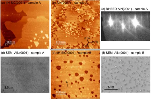
different reconstruction was identified on each terrace, thanks to atomic resolution studies. But if the Si beam flux is too high and the substrate temperature too low, the SiC(0001) surface is less homogeneous with the apparition of Si clusters and surface reconstruction domains of smaller area. In the NC-AFM of Fig.3(e)the dark holes have a height of around 1Å and the Si clusters appear as white dots pointed by the dark arrow. As shwon in the following, the homogeneity of the prepared SiC(0001) surfaces has a huge effect on the cristalline quality of the AlN layers.
AlN sample A (Fig. 3(b),3(c),3(d)) was grown on the SiC surface of Fig.3(a)and sample B (Fig.3(f)) on the SiC surface of Fig.3(e). The main difference compared to AlN layers grown on Si(111) is the absence of edge dislocations: only pairs of screw dislocations are visible on the NC-AFM images and hexagonal hillocks on the SEM images. The maximum dislocation density is ≃ 150/µm2, 2.5 times lower than for the best AlN layer grown on Si(111). The presence on
the SiC surfaces of Si clusters and of step edges has a direct influence on the hillocks density as observed on the SEM images: The less the surface is homogeneous, the more the hillocks density is raised. XRD measurements confirms this trend. For sample A the FWHM values for the (0002) and (10¯13) peaks are 370 and 610 arcsec, while they reach 1050 and 900 arcsec for sample B. By using an atomically flat (√3 ×√3 R30◦) reconstructed 4H-SiC(0001) surface, we succeeded
in reducing by a factor ≃2 the SD density (≃80/µm2) and to 0 the hillock density. In this case
the FWHM values for the (0002) and (10¯13) peaks decrease to 150 and 430 arcsec respectively. Compared to our best AlN layer grown on Si(111), these FWHM values are divided by a factor
FIG. 3. 200 nm thick AlN grown on 4H-SiC(0001): (a) - NC-AFM image of a 4H-SiC(0001) surface after 5 cycles of Si deposition. The steps are 1 Å high. (b) - NC-AFM image of a 200 nm AlN thick layer grown on the 4H-SiC(0001) sample shown in (a). (c) - RHEED pattern (15 KeV) of sample A along the [1010] axis after growth of the first 5 nm. (d): SEM image of the 200 nm AlN layer shown in (b). (e) - NC-AFM image of a 4H-SiC(0001) surface after 10 cycles of Si deposition. The dark arrow points on a Si cluster. (f) - SEM image of the AlN layer obtained on the 4H-SiC sample shown in (e). Image parameters : (a)-500×500 nm2, amplitude=5 nm, ∆f=-40 Hz; (b)-500×500 nm2, amplitude=5 nm, ∆f=-20 Hz; (d)-11×8 µm2;
067108-7 Chaumeton, Gauthier, and Martrou AIP Advances 5, 067108 (2015)
FIG. 4. 5 nm thick AlN grown on 4H-SiC(0001): NC-AFM image of the surface of 5 nm thick AlN(0001) layer grown on 4H-SiC(0001). The surface exhibits edge dislocations which are located at the interface between the crystalline domains A and B rotated by 180◦as shown by the triangular shape of the islands outlined with dashed lines. The dark lines indicate the
border between the domains. Image parameters: 500×500 nm2, amplitude=5 nm, ∆f=-5 Hz.
8 and 2 for the (0002) and (10¯13) peaks, confirming the better quality of the AlN layer grown on 4H-SiC(0001).
Thicknesses from 5 nm to 400 nm were studied. According to the RHEED pattern, the beginn-ing of the growth at 100 nm/h is 3D, and becomes 2D after the growth of 25 to 30 MLs. There is no significant reduction of the SD density between 200 nm and 400 nm grown in the same condition. However, for a very low growth rate (10 nm/h) of a 5 nm thin AlN layer, it is possible to reduce the SD density to ≃ 0/µm2. The sharp lines, the intensity and the Kikuchi lines of the RHEED pattern
displayed in the Fig.3(c) for such a layer indicate that the surface is extremely smooth and flat, which is confirmed by the NC-AFM image shown in Fig.4. This surface presents EDs visible on the NC-AFM images and also on the SEM images in Fig.5. Their origin will be discussed in the next section. Nevertheles, the areas between these EDs are atomically flat with a size that reaches (200 nm)2.
V. ORIGIN OF DEFECTS
Thanks to these two studies with high resolution NC-AFM images, it was possible to show that the first MLs of the growth have a direct influence on the hillock and the dislocation densities. For AlN grown on Si(111), the main origin of the dislocations is the in-plane lattice mismatch of 19 % between AlN(0001) and Si(111). This mismatch generates a high dislocation density located at the interface between the AlN layer and the Si substrate and may lead to an initial 3D growth. These dislocations propagate through the layer and terminate at the surface in the form of edge disloca-tions and pairs of screw dislocadisloca-tions. A thickness of about 50 nm is necessary to bury the initial 3D nucleation layer before reaching a 2D growth regime. After optimizing the growth parameters and the preparation of the Si(111)-(7 × 7) reconstructed surface, the minimum SD and ED densities induced by the lattice mismatch are about 200/µm2(2×1010/cm2).
For a 5 nm AlN layer grown on 4H-SiC(0001), the NC-AFM image of Fig. 4 shows that the EDs are mainly placed on the borders between crystallographic domains rotated by 180◦, as
shown by the orientation of the triangular islands on the same surface monolayer. These borders are usually called stacking mismatch boundaries (SMBs). They are induced by the polytype mismatch between 4H-SiC and 2H-AlN.4If the diffusion of species is efficient enough to allow the nucleation
FIG. 5. 5 nm thick AlN grown on 4H-SiC(0001): SEM images ((a) 32.5×24 µm2and (b) 3.2×2.4 µm2) of the AlN layer
shown in figure4. The white arrows point to EDs located along the nanometric steps of the 4H-SiC surface. The dark arrows point to the first stage of the formation of the hillocks shown in Fig.3(f).
SEM images of Fig. 5, lines of EDs pointed by white arrows are visible. Their orientation and their density are typical of the orientation and the step edge density of the initial 4H-SiC substrate. Besides these lines of EDs, there are aggregation of EDs pointed by dark arrows. We have observed after the growth of 200 nm of AlN a density of hillocks that is similar to the density of these ED aggregations, suggesting that the latter are the seeds for the former. Besides the presence of hillocks on the 200 nm thick AlN layer, no more EDs are observed on the NC-AFM images, but only pair of SDs. This indicates that the density of crystallographic domains growing up to the surface of the film is drastically reduced: locally, one domain expands at the expense of the other during the growth, leading to buried interfaces between the two types of domains, that are likely to generate threading dislocations appearing as pairs of SDs at the surface of the 200 nm thick layer. But compared to AlN layers grown on Si(111), the total SD density is always lower for 200 nm thick AlN layer, up to 10 times at ≃ 20/µm2(2×109/cm2).
VI. AlN(0001) GROWN AT 10 nm/h
The effect of a low growth rate of 10 nm/h on the surface roughness and on the dislocation density was studied by comparing two samples with thickness around 200 nm. For the first one the growth was realized with the usual protocol at 100 nm/h during 2 hours followed by 30 min at 10 nm/h. For the second one a starting layer was realized with a growth rate of 10 nm/h during 30 min and then the same growth sequence as for the first sample. As expected, the end of the growth at 10 nm/h reduces the overall roughness of the surface (fig6(b)and6(d)) with island and hole densities decreased by at least a factor of five compared to the surface obtained at 100 nm/h presented in figure3(b). Such smooth surfaces with atomically flat terraces of several hundred of
067108-9 Chaumeton, Gauthier, and Martrou AIP Advances 5, 067108 (2015)
FIG. 6. AlN grown on 4H-SiC(0001): RHEED pattern after the growth of 1 ML at 100 nm/h (a) and 10 nm/h (c) ; NC-AFM topography images of AlN(0001) layer after growth during 2 hours at 100 nm/h and 30 min at 10 nm/h (b) and with a starting growth layer at 10 nm/h during 30 min (d). Image parameters: (b) 500×500 nm2, amplitude=5 nm, f
0=285 kHz, ∆f=-15 Hz;
(d) 500×500 nm2, amplitude=5 nm, f
0=271 kHz, ∆f=-30 Hz.
square nanometers are suitable for the growth of thin quantum well and the formation of quantum dots induced by thickness fluctuations as already observed on Al1−xGaxAs/GaAs quantum wells.18
The main effect of a low growth rate is observed on the dislocation density, when the growth is started at 10 nm/h during 30 min. In these conditions, the SD density is around 20/µm2(fig6(d)),
five times lower than for films started at 100 nm/h (fig6(b)). This improvement of the layer quality can be explained by the diminution of the nucleation density during the first monolayer growth. This effect is observed on the RHEED patterns after the growth of 0.9 ML : While the pattern obtained for a growth rate of 100 nm/h (fig6(a)) shows a 3D behavior, the one at 10 nm/h (fig6(c)) shows a perfect 2D layer. The low growth rate of 10 nm/h allows to begin the 2D growth after the first ML while more than 25 MLs are necessary for that at 100 nm/h.
For 10 nm thick layers grown at 10 nm/h, the influence of RIII/V equal to 1/30 or to 1/10
was also studied by increasing or decreasing the NH3 pressure while the Al beam flux remained
constant. The SD density stayed between 0 and ≃ 10/µm2and the general aspect of the surface was
not significantly affected.
VII. SUMMARY
The use of NC-AFM coupled under UHV to a MBE chamber dedicated to the growth of AlN layers by ammonia molecular beam epitaxy has offered a unique way to characterize the surfaces of the Si(111) or the 4H-SiC(0001) substrates and the surfaces of the AlN layers grown on them in different conditions. The terminations of threading dislocations and their density can be rapidly determined and correlated to the surface conditions of the substrate and the growth parameters. Coupling these in-situ images to ex-situ SEM images allowed us to show the origin of threading dislocations in AlN(0001). For AlN layers grown on Si(111), the remaining nanodots on the Si(111) surface do not seem to have an impact on the dislocation density and therefore dislocations are mainly induced by the in-plane lattice mismatch of 19 % between AlN(0001) and Si(111). By optimizing the preparation of the Si(111) surface and the growth parameters we obtained AlN layers with a terminating dislocation density of 2×10¹⁰/cm2and FWHM values for the XRD (0002)
and (10¯13) peaks of 1250 and 970 arcsec respectively. For 200 nm thick AlN layers grown on 4H-SiC(0001), no edge dislocations (ED) are visible at the surface. The 4H-SiC surface conditions impact mainly the hillock density generated by the aggregation of edge dislocations that appear at the beginning of the growth (5 nm). Others EDs related to the stacking fault boundaries (SMBs)
are aligned mainly along the step edges of the 4H-SiC surface. They are burried after 200 nm growth where only SD dislocations are visible at the surface. By decreasing the growth speed from 100 nm/h to 10 nm/h at the beginning of the growth and continuing with the normal growth speed of 100 nm/h, the terminating dislocation density can be decreased to its lower value of 2×10⁹/cm2and
the FWHM values for the XRD (0002) and (10¯13) peaks are also decreased to 150 and 430 arcsec respectively.
ACKNOWLEDGMENTS
The authors thankfully acknowledge S. Vézian, F. Semond, B. Damilano, Y. Cordier and J. Massies from the CRHEA for their great help in transmitting us their AlN growth protocol. We also thank M. Portail for the SiC H2gas etching, Nicolas Ratel-Ramond from CEMES for X-ray
measurements, and engineers from the AIME for cutting Si and SiC wafers. This work is supported by the European Commission within the projects AtMol (contract N◦ ICT-270028) and PAMS
(contract N◦ICT-610446).
1S. Dasgupta, F. Wu, J. S. Speck, and U. K. Mishra,Applied Physics Letters94, 151906 (2009). 2J. C. Moreno, Thèse Ph.D. thesis, UNIVERSITE de Nice-Sophia Antipolis, 2009.
3H. Behmenburg, C. Giesen, R. Srnanek, J. Kovac, H. Kalisch, M. Heuken, and R. Jansen,Journal of Crystal Growth316,
42 (2011).
4H. Okumura, M. Horita, T. Kimoto, and J. Suda,Applied Surface Science254, 7858 (2008). 5X.-Q. Shen, M. Shimizu, and H. Okumura,Japanese Journal of Applied Physics42, L1293 (2003). 6A. Matsuse, N. Grandjean, B. Damilano, and J. Massies,Journal of Crystal Growth274, 387 (2005).
7Y. Lu, X. Liu, X. Wang, D.-C. Lu, D. Li, X. Han, G. Cong, and Z. Wang,Journal of Crystal Growth263, 4 (2004). 8G. Koblmueller, R. Averbeck, L. Geelhaar, H. Riechert, W. Hosler, and P. Pongratz,Journal of Applied Physics93, 9591
(2003).
9B. Zhang, M. Wu, X. Shen, J. Chen, J. Zhu, J. Liu, G. Feng, D. Zhao, Y. Wang, and H. Yang,Journal of Crystal Growth
258, 34 (2003).
10J. N. S. C. Jain, M. Willander, and R. V. Overstraeten,Journal of Applied Physics87, 965 (2000). 11S. Vézian, J. Massies, F. Semond, N. Grandjean, and P. Vennéguès,Physical Review B61, 7618 (2000). 12T. R. Albrecht, P. Grütter, D. Horne, and D. Rugar,Journal of Applied Physics668(1991).
13F. J. Giessibl,Science267, 68 (1995).
14W. Kern,J. Electrochem. Soc.137, 1887 (1990).
15A. Le Louarn, S. Vézian, F. Semond, and J. Massies,Journal of Crystal Growth311, 3278 (2009). 16S. Vézian, a. Le Louarn, and J. Massies,Journal of Crystal Growth303, 419 (2007).
17J. C. Moreno, “Etude de la croissance et des propriétés de films minces d’AlN épitaxiés par jets moléculaires sur substrat
silicium : application aux résonateurs acoustiques et perspectives d’hétérostructures intégrées sur silicium,” Ph.D. thesis (Université de Nice-Sophia Antipolis, 2009).

![FIG. 2. AlN(0001) grown on Si(111) : (a) - RHEED pattern (15 KeV) along the [1120] axis of a 10 nm thick AlN layer at the beginning of the growth](https://thumb-eu.123doks.com/thumbv2/123doknet/13707146.434069/6.891.313.580.130.742/fig-grown-rheed-pattern-thick-layer-beginning-growth.webp)