HAL Id: tel-02406272
https://tel.archives-ouvertes.fr/tel-02406272
Submitted on 12 Dec 2019
HAL is a multi-disciplinary open access archive for the deposit and dissemination of sci-entific research documents, whether they are pub-lished or not. The documents may come from teaching and research institutions in France or abroad, or from public or private research centers.
L’archive ouverte pluridisciplinaire HAL, est destinée au dépôt et à la diffusion de documents scientifiques de niveau recherche, publiés ou non, émanant des établissements d’enseignement et de recherche français ou étrangers, des laboratoires publics ou privés.
Fabrication and investigation of III-V quantum
structured solar cells with Fabry-Pérot cavity and
nanophotonics in order to explore high-efficiency
photovoltaic concepts : towards an intermediate band
assisted hot carrier solar cell
Benoît Behaghel
To cite this version:
Benoît Behaghel. Fabrication and investigation of III-V quantum structured solar cells with Fabry-Pérot cavity and nanophotonics in order to explore high-efficiency photovoltaic concepts : towards an intermediate band assisted hot carrier solar cell. Materials Science [cond-mat.mtrl-sci]. Université Pierre et Marie Curie - Paris VI, 2017. English. �NNT : 2017PA066729�. �tel-02406272�
Université Pierre et Marie Curie
Ecole doctorale de Physique et Chimie des Matériaux
Institut de Recherche et Développement sur l’Énergie Photovoltaïque (IRDEP, Chatou)
Centre de Nanosciences et de Nanotechnologies (C2N, Paris-Saclay)
Japanese-French Laboratory for Next generation Photovoltaic Cells (NextPV, Tokyo)
Fabrication and investigation of III-V quantum structured
solar cells with Fabry-Pérot cavity and nanophotonics
in order to explore high-efficiency photovoltaic concepts
Towards an intermediate band assisted hot carrier solar cell
Par Benoît Behaghel
Thèse de doctorat de Physique
Dirigée par Jean-François Guillemoles et Stéphane Collin
Présentée et soutenue publiquement le 18 décembre 2017
Devant un jury composé de :
Christian SEASSAL
Directeur de Recherche (INL, Lyon)
Rapporteur
Guilhem ALMUNEAU
Chargé de Recherche (LAAS, Toulouse)
Rapporteur
Christophe SAUVAN
Chargé de Recherche (LCF, Paris-Saclay)
Examinateur
Alexandra FRAGOLA
Maître de conférences (UPMC, Paris)
Examinateur
To Paker, Fr. Bernard and Léon, To all my family and friends, So that we can use our energy better.
Our duty as men is to act as though there were no limit to our power.
— Pierre Teilhard de Chardin s.j.
Acknowledgements
Acknowledgements
This manuscript present the work of a scientific collaboration between Japan and France. Behind all collab-orations there is the story of people interacting with each others. It is at the same time a challenge and a chance and I want to acknowledge all the people who helped to write this story.
First I want to thank my supervisors Stéphane Collin and Jean-François Guillemoles for their support and trust. They taught me that it is important to be rigorous and humble in your own work while being benevo-lent and patient towars others. Then I want to thank Professor Yoshitaka Okada who welcomed me very warmly in his lab and Pierre Destruel who triggered the creation of the Japanese-French laboratory “NextPV”. In Japan I discovered a different way of doing research however I felt the same core feeling of respect and dedication towards science. This experience would not have been possible without the support of the Monbukagakusho scholarship I received from the Japanese Ministry of Education, Culture, Sports, Science and Technology (MEXT). I want to thank all the people from the Japanese embassy in France, espe-cially Akiko Ishii-Foret for her kindness and all the staff from Tokyo University who made my stay conforta-ble. For the French side, I thank my doctoral school (ED 397) and UPMC administration for their under-standing of my specific situation between France and Japan. For the PhD defense, I want to thank Christian Seassal and Guilhem Almuneau for the reviewing of this work, the time they spent and their questions. I also thank the other jury members Alexandra Fragola and Christophe Sauvan for attending and judging my work. I am glad to have been accepted as a Doctor by the scientific community. I have learned to respect researchers and I think most of them have a good balance between their dreams, their science integrity and their duty towards our society. I thank them for giving me the opportunity to grow in this environment, learning and confronting ideas through conferences and publications.
I had the chance to work with three different laboratories. The first one was the C2N (ex-LPN). After all this time I realize how lucky I was to have been trained there. In term of clean room and nanofabrication it is a dream place. I want to thank Christophe Dupuis who is always ready to help anyone and does not hesitate to share his knowledge with a smile. He is (and will always be in my heart) a great soccer player. Throught soccer I met a lot of people and it was easier afterwards to interact because we shared playing under snow or heat waves. I want to thank Stéphane Guilet ninja and plasma warrior, Lorenzo Bernardi and Olivier Oria both being genius goal keepers and great support for IT. Kamel Merghem for his great audio sportcaster, dribbling and microbonding skills. Dominique Mailly as an endurant forward but also one of the coolest director I met. In the younger generation, Michaël Verdun, Juan Castro, Faycal Bai you were my greatest support on the soccer field and in the lab. Thanks for keeping up the positive attitude even under harsh situations that we all met at some point. In the PV team, I would like to thank first my sempai when I came in the group: Inès Massiot, Clément Colin and Nicolas Vandamme. I know I was sometime a bit annoying
Acknowledgements
iii
pan. She also taught me a lot about the art of capoeira and the difficulty of being a young mum. Talking about mum, I would like to thank Nathalie Bardou, Emilie Steveler and Cécile Joulaud who were always ready for advice and discussions fueling my motivation. About daddy advices, I will remember the discus-sions with Gregory Vincent, Fabrice Oehler, Andrea Scaccabarozzi and especially Andrea Cattoni who helped me to grow as a nanoimprinter but also gave me tips about many other things. I won’t forget also the BANG master Clément Tardieu and many participants like Christelle Tuambilangana, Ludivine Emeric, Jihene Zribi, Romaric de Lépinau, Louis Gouillart, Daniel Pelati, Ahmed Ben Slimane and Amadeo Michaud (also great soccer players). In the young generation, I want to thank particularly Hung-Ling Chen who helped a lot at C2N, IRDEP and with NextPV. I wish him good luck for his last year of PhD. I also wish the best to Thomas Bidaud who worked with NextPV and is now starting a PhD in C2N. The Japanese-French collaboration needs motivated students that can make the link between France and Japan. In this perspec-tive, I also want to thank Maxime Giteau who has been working at C2N and is now starting his PhD in Japan at NextPV. I also want to thank Fabrice Pardo and Jean-Luc Pelouard for some coffee discussions. I thank Xavier Lafosse and Alan Durnez for their help in teaching me about dielectric deposition, ellipsometry and reflectometry measurements. Laetitia Leroy and Laurent Couraud for metal depositions, Abdelmounaim Harouri for UV lithography and Jean-Claude Esnault for his dedication to the clean room. I thank Alain Péan for his tireless energy to fix many issues in the 2nd floor of our building not only computer stuff. Also I want
to thank Agnès Roux for helping me dealing with administrative papers. I don’t forget the adorable twin combo from Klearia: Anne-Claire Louër and Guillaume Da Rold who helped me and entertained me a lot in the clean room. Finally I cannot name all people of C2N but I want to give a general thank to this excep-tional research center and the great people I met there.
For my second year of PhD, I moved to Japan in NextPV on Komaba campus. There I found a new environ-ment and I can say here again that I was very lucky. The diversity of scientific topics on this campus is al-most unlimited. First I want to thank the Japanese professors who helped me get confortable in this new place: Masakazu Sugiyama, Yoshiaki Nakano and Takaya Kubo. In Okada lab, I was first welcomed by Hoshii-san. I thank him for always being keen to answer my numerous questions. Regarding the clean room envi-ronment and substrate removal, I want to thank Miyashita-san for Okada lab and Watanabe-san for Sugiyama lab. Both were patients and cautious with my training. In term of characterization, Tamaki-san introduced me to many setup. I want to thank him especially for his rigorous, tenacious and honest mind which was essential to improve my work and attitude towards science. I want to thank Shoji-san for his dedication in growing good samples for me and also for staying very late with me for discussion and some-times playing games after hard work to release the stress. I thank Sogabe-san and Yoshida-san for advising me on the modelisation and simulation. I thank Ahsan-san for introducing me to the photoreflectance set-up and for the good company everytime we had the chance to discuss. In Okada lab and Sugiyama lab, I also want to thank Ogura-san, Sodabanlu-san, Wang-san for the nice discussion and also the students Bern-san, Hung-Bern-san, Naito-Bern-san, Osawa-Bern-san, Shimomura-Bern-san, Mori-Bern-san, Yamashita-san and especially Inoue-san and Champ for their help in many aspects. I won’t forget also Fujiki-san and Hosaka-san for their kind help, I thank them for being such good Japanese mama for me. In NextPV, I also had the opportunity to work with people from the French part of the collaboration. First I would like to thank Ludmila Cojocaru for being such a great example for us. I thank Amaury Delamarre for helping me getting installed in Tokyo and also on many scientific aspects. I also want to thank Zacharie Jehl for sharing his experience in Japan and in many field of science, especially the science of boxing and hiking. Last but not least, I want to thank Lea Tatry and Anatole Julian who did long internship with us and produced great results for the collaboration but also participated to the good mood in the lab.
Acknowledgements
After I returned to France, I was given the opportunity to work more closely with IRDEP laboratory and especially the advanced characterization team. First I want to thank Laurent Lombez for always welcoming me in his team with a positive mood and sometime great jokes. Big up to Pierre Rale for the great work and many debates we had together. I thank Myriam Paire for her wise advices. François Gibelli and Dac-Trung Nguyen for great discussions on PL fitting and hot carriers. Florian Proise, Jean Rodière, Sébastien Jutteau and Gilbert El-Hajje as PhD comrades. I thank Enrique Leite for helping with many things in the characteri-zation room. I also thank Adrien Bercegol, Baptiste Bérenguier, Daniel Ory, Ombline Lafont and Jean Rous-set for the numerous coffee breaks and discussions after lunch. I hope IPVF will be a great success for French PV research and industry. Finally I want to thank Daniel Lincot for accepting me in his lab and Claire Vialette for her continuous support all along my PhD.
My last thanks are for my friends and family who shared my joys and sometimes my frustrations. I want to thank my two sisters: Solène and Anne-Colombe, my three brothers: Amaury, Ghislain and Louis-Marie, my in-laws: Bruno, Anne-Laure, Astrid and Théau and of course their children: Corentin, Alix, Aurore, Klervie, Xavier, Nour-Marie, Maxime, Aliénor, Augustin and Victoire. I want to thank my parents for their uncondi-tionnal support and my grandmother Magny for being an example of tenacity.
Abstract
Abstract
In the past decade, photovoltaics (PV) has become a key player for the future of worldwide energy genera-tion. Innovation in PV is likely to rely on high efficiency PV with flexible and lightweight thin films to enable PV deployement for mobile applications. In the framework of the Japanese-French laboratory “NextPV”, this thesis investigates the development of III-V quantum structured solar cells to explore high-efficiency photovoltaic concepts especially intermediate band solar cells (IBSC). Quantum structured IBSC have prov-en to be limited by thermal escape at room temperature and by low subbandgap light absorption. Follow-ing a consistent approach, we evaluate the topology, thermal escape mechanism, quantum structure and optical absorption of In(Ga)As quantum dots in a wide gap Al0.2GaAs host material. We also characterize
quantitatively the device operation and improve the optical design. For a high irradiation, we evidence a hot carrier population in the quantum dots. At the same time, sequential two-photon absorption (S-TPA) is demonstrated both optically and electrically. We also show that S-TPA for both subbandgap transitions can be enhanced by a factor x5-10 with light management techniques, for example by implementation of Fab-ry-Perot cavities with the different epitaxial transfer methods that we developed. More advanced periodi-cal nanostructures were also fabricated in the case of multi-quantum well solar cells using nanoimprint lithography techniques. Overall we discuss the possibility of realizing intermediate-band-assisted hot-carrier solar cells with light management to open the path for high-efficiency quantum structured IBSC.
Key words: photovoltaics, thin films, quantum structures, high efficiency, light management,
Résumé
Résumé
Le photovoltaïque (PV) s’est imposé comme un acteur majeur de l’énergie. L’innovation dans ce domaine passera sans doute par le PV à haut rendement sur des couches minces flexibles et légères permettant son déploiement dans les applications mobiles. Cette thèse étudie le dévelopement de cellules solaires III-V à structures quantiques visant des concepts PV hauts rendements tels les cellules solaires à bande intermé-diaire (IBSC). Ces IBSC se sont montrés limités du fait de l’échappement thermique des porteurs à tempéra-ture ambiante ainsi que la faible absorption optique sous le gap. Nous avons évalué la topologie, le méca-nisme d’échappement thermique, la structure quantique ainsi que l’absorption de boites quantiques en In(Ga)As dans un matériau hôte en Al0.2GaAs à grand gap. Nous avons aussi caractérisé de manière
quanti-tative comment opère ce système et avons amélioré son design optique. Sous une forte irradiation, nous avons mis en évidence l’apparition d’une population de porteurs chauds dans les boites quantiques. Par ailleurs, l’effet d’absorption sequentielle à deux photons (S-TPA) a été démontré. Nous avons observé une augmentation de ce S-TPA d’un facteur x5-10 grâce à du management de la lumière réalisé notamment avec des cavités de Fabry-Pérot. Des nanostructures périodiques ont aussi été fabriquées dans le cas de cellules solaires à multi-puits quantiques par l’utilisation de lithographie en nanoimpression. Dans l’ensemble cette étude vise à discuter la possibilité de réaliser des cellules solaires à porteurs chauds assis-tés d’une bande intermédiaire et améliorées par un management optique afin d’ouvrir la voie pour des cellules à hauts rendements.
Mots clés: photovoltaïque, couches minces, structures quantiques, haut rendement, management optique,
Résumé
ix
Dans ce travail de thèse nous explorons le domaine des nouveaux concepts pour le photovoltaïque, en par-ticulier, pour le dévelopement d’une nouvelle génération de cellule solaire à haut rendement. Pour cela nous avons participé à la fabrication et à l’étude des hétérostructures III-V semiconductrices contenant des structures quantiques. Ce travail de thèse s’est déroulé dans le cadre du laboratoire international associé (LIA) « NextPV » hébergé au « Research Center for Advanced Science and Technology » (RCAST) de l’Université de Tokyo, en collaboration avec deux laboratoires du CNRS : le Centre de Nanosciences et de Nanotechnologies (C2N) ainsi que l’institut de recherche et développement sur l’énergie photovoltaïque (IRDEP) faisant maintenant partie de l’Institut Photovoltaïque d'Ile-de-France (IPVF).
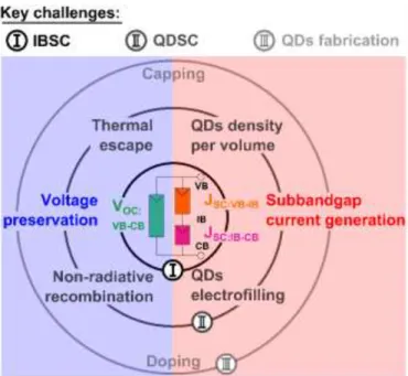
Le chapitre 1 constitue une introduction sur le sujet du photovoltaïque ainsi que les possibilités pour le haut rendement, en particulier pour le domaine spécifique des cellules solaires à bandes intermédiaires (IBSC). L’apport du management de la lumière est précisé essentiellement pour promouvoir l’absorption, naturellement faible dans les nanostructures quantiques. En illustration de ce chapitre, il peut être intéres-sant de commenter la Fig. i ci-dessous qui résume les challenges clés liés à la fabrication de ces cellules. Ces challenges peuvent être séparés en trois parties. En premier lieu, ceux qui sont directement relatifs au fonctionnement d’une IBSC. D’un côté la préservation d’un voltage au même niveau qu’une cellule clas-sique simple jonction doit être réalisée. Et de l’autre, un courant additionnel venant de l’absorption se-quentielle de deux photons sous le gap doit être assuré via l’introduction de la bande intermédiare. Dans le cadre spécifique des cellules solaires à boites quantiques (QDSC), plusieurs problèmes interviennent relati-vement à ces deux challenges. D’un côté, l’échapement thermique des porteurs venant des boites ainsi que le fort taux de recombinaisons non-radiatives pénalisent la préservation du voltage. De l’autre, la faible densité volumique des boites dans les couches quantiques ainsi que le faible niveau de remplissage de la bande intermédiaire ne permettent pas une absorption efficace de photons sous le gap. Enfin toutes ces problématiques sont intrinséquement liées aux conditions de fabrication de ces boites. Nous citons en exemple deux procédés permettant d’améliorer les proprités de nos IBSC, la technique du « capping » ou recouvrement et la technique de dopage des boites quantiques.
Fig. i: Schéma explicatif résumant les challenges clés liés à la fabrication de cellules solaires à bande intermédiaires fabriqués à l’aide de boites quantiques.
Résumé
Dans le chapitre 2, nous introduisons les principales étapes technologiques nécessaires à la réalisation de nos cellules. Nous expliquons notamment les technologies de report sur substrat hôte que nous avons utili-sé ainsi que les différentes étapes de nanostructuration. La Fig. ii, donne une vision d’ensemble du process flow.
Fig. ii: Schéma du process flow résumant les différentes étapes de fabrication menant à la realisation d’une cellule solaire à boites quantiques avec nanostructuration (ici en face avant).
Tout d’abord, (1) la jonction p-i-n avec les structures quantiques est crû sur un substrat en GaAs dopé n avec une couche « etch STOP layer » pour la phase de transfert de substrat. En (2), les contacts métalliques localisés en face arrière sont effectués par enrésinement, lithographie UV, dépôt de métal et lift-off et la couche de contact en GaAs dopé p est gravée. En (3), un dépôt de mirroir est effectué puis un collage sur un substrat de verre est fait à l’aide d’une résine photosensible. En (4), le substrat en GaAs est gravé
sélec-Résumé
xi
tuée de la même manière que pour les contacts arrière. En (6), l’étape de « mesa » est réalisée qui consiste à isoler les cellules solaires les unes des autres en les protégeant avec de la résine et en gravant entre. En (7), une couche de TiO2 est déposée. En (8), l’étape de nanostructuration en face avant est effectuée à
l’aide de plusieurs étapes décrites au chapitre 2. Enfin en (9), le reste du TiO2 déposé est retiré des contacts
pour pouvoir effectuer la caractérisation éléctrique des cellules.
Dans le chapitre 3, le design et le fonctionnement des IBSC à boites quantiques semiconductrices sont in-troduits en particulier avec les matériaux constitués de boites quantiques d’In(Ga)As avec matrice en Al0.2Ga0.8As. Nous signalons aussi l’influence de facteurs comme la concentration en boites quantiques sur
le mécanisme d’absorption séquentielle à deux photons et le rôle clé que peut jouer à cet égard la concen-tration du champ électromagnétique par piégeage optique. Les procédés de croissance épitaxiale sont briè-vement décrits, ainsi que la topographie des nanostructures obtenues. Une étude plus approfondie sur les mécanismes d’échappement et de collecte des porteurs est ensuite présentée. Les mesures de photolumi-nescence résolue en température, présentées dans la Fig. iii, permettent notamment de mettre en évi-dence un régime d’échappement et de transfert par saut et relaxation vers les boîtes quantiques les plus grandes.
Fig. iii: Mesure de photoluminescence en temperature mettant en évidence une transition dans les boites à partir de T > 100 K. L’on passe d’un régime où les porteurs sont « gelés » à un régime où ils peuvent « sauter » de boites en boites.
Des mesures électriques ont par ailleurs mis en évidence l’impact des défauts dans la matrice d’AlGaAs sur les mécanismes de transport et d’échappement des porteurs. Enfin nous avons essayé d’étudier de ma-nière précise l’absorption dans ces structures quantiques de plusieurs mama-nières, notamment de mama-nière expérimentale à l’aide d’une méthode interférentiel fondé sur l’utilisation de cavité de Fabry-Pérot à l’aide de différentes épaisseurs de diéléctriques positionnées en face avant comme réprésenté dans la Fig. iv. Des « marches » en diélectriques (SiNx) sont effectuées sur le dessus de la surface des couches reportées sur
miroir afin de créer des cavités de Fabry-Pérot d’épaisseur différentes comme cela est indiqué sur le sché-ma ainsi que la photo au microscope. Ces différentes épaisseurs de cavité induisent des résonances posi-tionnées à différents endroits spectralement, que l’on remarque sur les spectres de réflectométrie. En fit-tant ces courbes on est en mesure de remonter à la valeur de l’absorption sur la plage du spectre balayé par le décalage de ces pics de résonances.
Résumé
Fig. iv: Principe de l’interférométrie de Fabry-Pérot pour la caractérisation de l’absorption. Des « marches » en diélectriques (SiNx)
sont effectuées sur le dessus de la surface des couches reportées afin de créer différentes cavités de Fabry-Pérot d’épaisseur diffé-rentes comme cela est indiqué sur la photo au microscope. Ces diffédiffé-rentes épaisseurs de cavité induisent des résonances position-nées à différents endroits spectrallement, que l’on remarque sur les spectres de réflectométrie. En fittant ces courbes on est en mesure de remonter à la valeur de l’absorption sur la plage du spectre balayé par le décalage de ces pics de résonances.
Résumé
xiii
Le chapitre 4 présente une étude de la dynamique de la bande intermédiaire constitué par les états quan-tiques formés dans les boites. Un ensemble de caractérisations opquan-tiques est présenté, en vue d’évaluer les paramètres importants des cellules solaires à boites quantiques. Il s’agit notamment des facteurs d’idéalité, des effets de saturation des niveaux des boîtes, et de la mise en évidence de populations possiblement indépendantes entre boîtes et milieu hôte. Lorsque la concentration de porteurs dans les larges boites quantiques atteint le niveau de semiconducteurs dégénérés, un régime de porteurs chauds semble pouvoir apparaître. Cette population chaude semble avoir un effet thermoelectrique qui sépare le potentiel chi-mique dans le matériau hôte de celui dans les boites quantiques permettant ainsi d’isoler la bande inter-médiaire lorsque celle-ci se retrouve à moitié remplie. Cette interprétation s’appuie notamment sur l’analyse de la Fig. v. Ces graphes représentent l’évolution de la température d’une part (gauche) et celle de la séparation des quasi niveaux de Fermi (QFL) d’autre part (droite) en fonction de l’excitation laser pour la population de porteurs dans les boites quantiques et celle dans la wetting layer (WL) et le matériau hôte. L’augmentation en température des porteurs dans les boites semblent suivre une loi d’Arrhénius avec une énergie d’activation (Ea) d’envrion 250 meV tandis que la température dans le matériau hôte semble rester
à tempérautre ambiante. Cette différence en température semble conduire à la séparation des QFL jusqu’à une valeur de 140 meV.
Fig. v: Graphes représentant l’évolution de la température d’une part (gauche) et celle de la séparation des quasi niveaux de Fermi (QFL) d’autre part (droite) en fonction de l’excitation laser pour la population de porteurs dans les boites quantiques et celle dans la wetting layer (WL) et le matériau hôte. L’augmentation en température des porteurs dans les boites semblent suivre une loi d’Arrhénius avec une énergie d’activation (Ea) d’envrion 250 meV tandis que la température dans le matériau hôte semble rester à
tempérautre ambiante. Cette différence en température semble conduire à la séparation des QFL jusqu’à une valeur de 140 meV. Dans ce chapitre, nous étudions par ailleurs les propriétés relatives à l’absorption sequentielle de deux photons qui sont indispensables au fonctionnement des cellules solaires à bande intermédiaire. Ainsi nous démontrons la possibilité pour ces cellules de combiner à la fois le concept de bande intermédiaire et de porteurs chauds sous le nom de cellules solaires à porteurs chauds assistées d’une bande intermediaire (IB-HCSC). Nous évaluons les performances et perspectives de telles cellules qui pourraient fonctionner comme cellule à haut rendement à condition de disposer d’un matériau hôte de qualité optimisée et de pré-remplir les niveaux des boîtes (par capping ou dopage).
290
340
390
440
490
540
1E-4 1E-3 1E-2 1E-1 1E+0 1E+1
T
C(K)
Laser excitation (mW)
QDs
WL and host
Ea= 250 meV1.05
1.10
1.15
1.20
1.25
1.30
1.35
1.40
1E-4 1E-3 1E-2 1E-1 1E+0 1E+1
Dµ
(eV
)
Laser excitation (mW)
Résumé
Le cinquième et dernier chapitre concerne l’utilisation de résonances optiques, qu’elles soient simples comme dans le cas de Fabry-Pérot verticaux ou plus complexe comme avec des réseaux périodiques à deux dimensions réalisés à l’avant ou à l’arrière de la cellule. Ces effets sont étudiés dans le cas de matériaux à base de multi-puits quantiques et de matériaux à base de boites quantiques. On observe un effet de l’augmentation du courant de court-circuit, qui est reliée à l’absorption dans les structures quantiques. Les possibilités d'augmenter le rendement au-delà, au travers du positionnement optimal des structures quan-tiques est discuté pour la structure à puits et illustré dans la Fig. vi.
Fig. vi: Illustation de l’effet du positionnement des structures quantiques. Dans le cas (b), la zone des multi-puits est divisée en trois parties pour correspondre parfaitement aux maxima du champ éléctrique de la lumière incidente. Cela induit directement un gain dans l’absorption comme cela est illustré sur les spectres d’absorption.
Dans le cas des structures à boîtes quantiques, dont l’absorption initiale est très faible aux grandes lon-gueurs d’onde, une stratégie exploitant des structures métal-isolant-métal (MIM) est proposée. Cette struc-ture, présente une efficacité qui n’est pas suffisante au regard de l’augmentation nécessaire dans les pré-sentes structures. Cette augmentation ne peut être obtenue qu’au travers d’une grande densité de réso-nances à fort facteur de qualité.
Résumé
xv
En conclusion de ce manuscrit, nous établissons un certain nombre d’idées et de perspectives pour le futur des ces cellules. Tout d’abord, nous pensons que l’effort devrait être en priorité porté sur l’aspect fabrica-tion des boites quantiques notamment en essayant d’avoir un matériau hôte présentant moins de défauts afin d’avoir une efficacité radiative du même ordre qu’une cellule simple jonction III-V à l’état de l’art. En deuxième axe, l’étude du dopage des boites quantiques semblent être aussi important afin d’essayer de préremplir avec des porteurs dans l’optique d’avoir un niveau d’apparition des porteurs chauds pour des niveaux d’irradiation moins élevé. Il est aussi intéressant de noter qu’un fort dopage des boites pourrait peut-être conduire à réaliser des objets optiques exotiques intéressants de type « relai plasmonique » en utilisant des effets de couplage plasmonique dans le proche infrarouge. Enfin, niveau fabrication, il paraît essentiel de s’orienter vers des structures quantiques plus denses dans la direction de croissance afin de gagner sur le plan de l’absorption. En terme de dispositif optoéléctronique, l’idée d’aller vers une cellule sans jonction composée seulement de boites quantiques avec des contacts sélectifs couplé à une structure MIM paraît intéressante pour maximiser le ratio de structure quantique par rapport à l’épaisseur totale de la couche absorbante ainsi que dans l’idée d’avoir un photofilling pour le concept de cellules IBSC à por-teurs chauds. Enfin, toutes ces approches doivent être étudiées dans le cadre du développement de cel-lules solaires flexibles, légères et bas coût. Ainsi le dévelopement des techniques de transfert déjà com-mencé dans ce sens doit être prolongé. En suivant un certain nombre des pous pensons que pour les dix prochaines années, il pourrait y avoir une cellule IBSC à porteurs chauds à simple junction qui dépasse la barrière symbolique des 30% de rendement.
Contents
Contents
Acknowledgements ... iii Abstract ... vi Résumé ... viii General introduction ... 20Introduction to photovoltaics and light management ... 24
1.1 Photovoltaics: towards high-efficiency solar cells ... 24
1.1.1 Principle of photovoltaic conversion of solar energy ... 24
1.1.2 Novel concepts for high-efficiency PV conversion of solar energy ... 30
1.2 Light management for quantum-structured IBSCs ... 38
1.2.1 Lambertian scattering PV light trapping ... 38
1.2.2 Application to quantum-structured solar cells ... 40
Conclusion ... 48
Fabrication and nanofabrication for quantum structured solar cells ... 50
2.1 Sample fabrication ... 50
2.1.1 Stacking design and growth ... 50
2.1.2 Device fabrication ... 55
2.1.3 Additional processes ... 59
2.2 Epitaxial transfer processes ... 62
2.2.1 Etch stop layer technique ... 62
2.2.2 Sacrificial layer technique ... 65
2.3 Nanofabrication ... 68
Contents
xvii
QD-IBSC system: from ideal to experimental PV material ... 76
3.1 Description of QD-IBSCs system for light management implementation ... 76
3.1.1 Choice of material: In(Ga)As QDs in Al0.2GaAs host material ... 76
3.1.2 Position of QD layers ... 82
3.2 Fabrication of QDs absorber suitable for IBSCs ... 86
3.2.1 Growth of QDs by MBE ... 86
3.2.2 Control and improvement of QDs growth ... 92
3.3 Investigation and modeling of QDs properties ... 106
3.3.1 QDs interactions with host material: thermal and electrical properties ... 106
3.3.2 Simulation of different QDs: shape, aspect ratio, QWIs, WL, In content ... 122
3.4 QDs absorption: simulation and experimental determination ... 130
3.4.1 Absorption from k.p calculation ... 130
3.4.2 Absorption measurements ... 135
Conclusion ... 146
Intermediate band dynamic study to evidence novel PV concept ... 148
4.1 Calibrated photoluminescence ... 148
4.1.1 Characterization setup... 148
4.1.2 Balance of photons ... 150
4.1.3 Quasi-fermi level splitting ... 182
4.2 Two-color excitation photoluminescence ... 190
4.2.1 Characterization setup... 190
4.2.2 IR pump effect on photoluminescence ... 191
4.2.3 Steady-state rate equation model ... 199
4.3 Potential of a hot carrier thermally activated QD-IBSC or IB-HCSC ... 204
4.3.1 IB-CB QFL splittings ... 204
4.3.2 Fermi-Dirac distribution inside QDs... 205
4.3.3 Potential efficiency of a thermally activated QD-IBSC ... 206
Conclusion ... 210
Light management strategies applied to quantum-structured solar cells ... 214
5.1 Application to multi-quantum well solar cells ... 214
5.1.1 Fabry-Pérot cavity effect on MQW solar cells ... 214
Contents
5.2 Application to quantum dot solar cells ... 232 5.2.1 Fabry-Pérot effect on QDSCs ... 232 5.2.2 Nanopatterns strategy for QDSCs... 245 Conclusion ... 250 Conclusion and perspectives ... 252 Appendices ... 256 A. Fabrication protocols ... 256 B. InGaAs QD growth issues ... 260 C. Method to fit the PL from a QD ensemble ... 264 References ... 268
General introduction
General introduction
General introduction
In the past decade, growth of photovoltaics (PV) has followed an exponential curve making it a key player for the future of worldwide energy generation. PV manufacturing companies have been consolidating and more money is being invested in research and development (R&D). Innovation in PV is blooming in three directions: (i) the cost of the device, (ii) the energy efficiency gain and (iii) the ease of deployment via new PV architectures. On one hand, industrials compete and invest a lot of efforts to reduce the cost of PV modules, and at the same time, research on new materials like Perovskite seems to be promising to reduce production cost of a solar cell. On the other hand, research on high-efficiency PV is still in an exploratory phase and needs proof of concept in order to attract more attention. Finally, new PV architectures are be-ing developed thanks to flexible and lightweight thin-films. In the future, it is likely that high-efficiency PV with flexible and lightweight thin-films will become more conventional and unlock novel applications e.g. indoor PV, solar-powered vehicule, PV high altitude sky platforms, etc.
This thesis work is born thanks to the will of Japanese and French researchers to collaborate on PV up-stream concepts throught the creation of an international joint laboratory called “NextPV”. From the Japa-nese side, Okada and Sugiyama laboratories from the Research Center for Advanced Science and Technolo-gy (RCAST) of the University of Tokyo have brought their expertise in the realization of quantum-structured materials necessary to achieve promising high-efficiency PV concepts. On the other side, the French Na-tional Center for Scientific Research (CNRS) has contributed on the topic of nanophotonics and nanofabri-cation for thin-films via the Centre for Nanoscience and Nanotechnology (C2N). The CNRS Institute of Re-search and Development on Photovoltaic Energy (IRDEP) was also involved for advanced characterization. In the framework of this collaboration, my time was divided evenly between France and Japan, in particular thanks to the Monbukagakusho scholarship from the Japanese Ministry of Education, Culture, Sports, Sci-ence and Technology (MEXT) and the involvement of the Embassy of Japan in France.
In this thesis, we investigate III-V quantum-structured solar cells with light management strategies and nanofabrication for the realization of high-efficiency PV concepts. This solution has great potential to reach high-efficiency PV and has the advantage of having a less complex device structure compared to nowadays high-efficiency PV solutions. We believe that in the future it could become an economically viable light-weight, flexible and high-efficiency solution and we want to work towards a proof-of-concept solar cell to validate the theory and open the path for future investments.
General introduction
21
strategies in PV devices and especially we give examples of state-of-the-art investigations on quantum-structured solar cell.
In chapter 2, we describe the fabrication techniques that were involved all along our work. We cover the topic of the clean room microfabrication of PV devices and report on two epitaxial layer transfer methods that we developped and used in the framework of the “NextPV” collaboration. We also detail the technique that was used to implement nanophotonics at the C2N and we give a general process flow of a final solar cell fabricated during this thesis.
In chapter 3, we thoroughly investigate the physical properties of the main quantum-structured system that was used: the In(Ga)As / Al0.2Ga0.8As quantum dot (QD) system designed especially for high-efficiency
intermediate band solar cell (IBSC). We explain the target, design and material growth of such system that are being fabricated in Okada laboratory. We give details on basic characterization from a topological and morphological point of view. We also investigate thermal, electrical and optical properties by characteriza-tions and simulacharacteriza-tions.
In chapter 4, we demonstrate the potential of such systems for the realization of high-efficiency PV, espe-cially for the concept of intermediate band assisted hot carrier solar cells (IB-HCSCs). We use specific char-acterization techniques dedicated to the investigation of carrier and light dynamics and interactions in the In(Ga)As / Al0.2Ga0.8As QD system.
Finally, in chapter 5, we investigate the light management strategies that were implemented on quantum-structured solar cell. We optimize optical design by numerical calculations and fabricate nanopatterned structures at the back or the front to induce a multi-resonant photonic effect inside PV layers. Nanopat-terning was made only on multi-quantum well (MQW) solar cells fabricated in Sugiyama laboratory. Such quantum-structured solar cells are easier than QD solar cells in terms of growth control and physical inter-pretation. Fabrication, characterization, analysis and comparison of a simple Fabry-Pérot (FP) cavity effect is presented for QD solar cells.
This thesis presents results in many domains of experiments. Design and numerical simulations, material growth and fabrication in clean room, basic and advanced characterization and analytical or numerical fit-ting. I want to acknowledge here the different contributions to the work presented in this manuscript. The III-V quantum-structured layers were epitaxially grown at RCAST in Japan by Dr. Kentaroh Watanabe and Dr. Yasushi Shoji. Some of QDs AFM images were taken by Dr. Yasushi Shoji. PL at low temperature was done under the supervision of Dr. Ryo Tamaki. A special acknowledgment goes to Dr. Christophe Dupuis, Dr. Nicolas Vandamme and Dr. Naoya Miyashita, whose help and advice have been really appreciated along the different fabrication processes. I also had the pleasure to supervise and receive help from Lea Tatry during her 6-month Master’s internship on the development of epitaxial lift-off (ELO) transfer technique. All SEM images presented in this thesis have been taken at C2N by coworkers (Dr. Christophe Dupuis, Dr. Juan Castro, Dr. Alexandre Gaucher and Dr. Julie Goffard). The process of transfer using UV reticulation polymer glue was proposed by Dr. Andrea Cattoni. He also trained me to the nanoimprint lithography. The sol-gel TiO2 was provided by Dr. David Grosso and his team (LCMCP, Collège de France, Paris). The deposition of dielectric coatings on samples were supervised by Dr. Xavier Lafosse and Dr. Alan Durnez. Regarding char-acterization, the current-voltage (I-V) and external quantum efficiency (EQE) characterizations were made in RCAST, C2N or IRDEP. I-V at low temperature were done under the supervision of Dr. Zacharie Jehl. The calibrated PL and two-color excitation characterization presented in chapter 4 have been performed at
General introduction
IRDEP by Dr. Pierre Rale and Hung-Ling Chen. Data analysis, PL numerical fitting and interpretations have been done with the help of Dr. Pierre Rale, Hung-Ling Chen, Dr. Laurent Lombez, Dr. François Gibelli and Dr. Dac-Trung Nguyen. Optical numerical calculations have been performed using transfer matrix or Rouard’s method for simple FP cavity. In chapter 5, I used the Reticolo software provided by Dr. Philippe Lalanne and Dr. Christophe Sauvan (Institut d’Optique, Palaiseau) in order to investigate the effect of nanostructuration. Dr. Katsuhisa Yoshida and Dr. Tomah Sogabe helped me to better understand the 8-band k·p calculations made using nextnano software provided by Dr. Stefan Birner. I finally want to acknowledge the fruitful dis-cussions that we had with Dr. Amaury Delamarre, Dr. Nazmul Ahsan, Dr. Stéphane Guillet and Dr. Takuya Hoshii.
Introduction to Photovoltaics and light management
Introduction to Photovoltaics and light management
Introduction to photovoltaics and
light management
Photovoltaic technologies are becoming essential to the development of renewable energy pro-duction at world scale. Nowadays most of photovoltaics revolve around one economical and competitive solution, which has ensured a fast deployment of solar energy in the last decade. For many reasons, it is strategic and reasonable to keep pushing the research and development (R&D) towards other solutions that can offer more flexibility in the use of solar energy for the market. In this perspective, we propose to focus on the challenge of high-efficiency solar cells. In a first part, we describe the basic principle of photo-voltaics with the coming of novel concepts. We describe in particular the solution of an intermediate band solar cell (IBSC) based on III-V quantum-structured materials. All along the manuscript, we will see the many advantages and disadvantages of these materials. The development and emergence of new PV tech-nologies often necessitate the control of three phases: (1) control over the material fabrication and proper-ties, (2) control over the device fabrication and characterization, and finally (3) the control over optical or light management. For this reason, in a second part, we introduce and discuss the application of light man-agement for PV applications and especially for quantum-structured solar cells.
1.1
Photovoltaics: towards high-efficiency solar cells
In this first part, we introduce the origin and principle of PV in order to discuss the possibility of increasing its efficiency. We report on various innovative paths that are being investigated worldwide. In the frame-work of the French-Japanese International Joint Laboratory “NextPV”, we chose to focus on intermediate band solar cell (IBSC) concept based on III-V quantum-structured materials. We describe the core concept and underline the advantages and disadvantages of this approach.
1.1.1 Principle of photovoltaic conversion of solar energy
The photovoltaic effect has been first observed by French physicist Edmond Becquerel in 1839 throught his work on electrochemical cell [1]. It is defined as the creation of voltage or electric cur-rent in a material upon exposure to light. Later in 1940, with the advance of solid-state devices, semiconductor researchers at Bell Labs paved the route towards the nowadays-dominant silicon
p-n jup-nctiop-n techp-nology. Ip-n 1954, they demop-nstrated the first practical silicop-n solar cell with about 6%
efficiency at converting sunlight energy into electricity. In the sixties, Shockley and Queisser pro-posed a model to determine the theoretical efficiency limit [2]. At the same time as the rest of the scientific community, they evidenced the future routes towards higher efficiency [3].
Introduction to Photovoltaics and light management
25 1.1.1.1 Basic principle of PV conversion
i). Electron-hole pair generation in a two-level system
The photovoltaic effect is a fundamental effect that can be seen as the response of an ensemble of atoms under irradiation. As represented in Figure 1.1-1 (a), the representation of atoms by Bohr in-troduce the idea that positively charged atomic nucleus possess electrons jumping between orbits by emitting or absorbing electromagnetic energy: Δ𝐸 = ℎ𝜈 with ℎ the Planck constant and 𝜈 the ir-radiation frequency. More precisely, quantum mechanics band theory has been successfully used in solid-state physics to model the electronic structure of ensemble of atoms. It is especially true for periodic organization like crystals, which have specific electronic band structures.
Figure 1.1-1: (a) Bohr model of the hydrogen atom where the negatively charged electron confined to an atomic shell en-circles a small positively charged atomic nucleus. Electron jump between orbits is accompanied by an emitted or ab-sorbed amount of electromagnetic energy (hν). The orbits in which the electron may travel are shown as grey circles. (b) Filling of the electronic states in various types of materials at equilibrium. Here, height is energy while width is the density of available states for a certain energy in the material listed. The shade follows the Fermi-Dirac distribution (black = all states filled, white = no state filled). In metals, the Fermi level EF lies inside at least one band. In insulators and
semi-conductors, the Fermi level is inside a band gap between the valence and conduction bands. Adapted from Wikipedia. As represented in Figure 1.1-1 (b), in the case of semiconductor materials, a two-level system is usually used to model the electronic band structure with carrier filling of the electronic states fol-lowing a Fermi-Dirac distribution, represented with the shades (black = all states filled, white = no state filled). The bottom level is the valence band (VB) and is defined as the highest range of elec-tron energies in which elecelec-trons are normally present at absolute zero temperature. The upper lev-el is the conduction band (CB) and is defined as the lowest range of vacant lev-electronic states. In PV, the energy band gap between the two bands is used to absorb the electromagnetic energy irradia-tion to promote an electron from VB to CB. This phenomenon creates an electron-hole pair harvest-ing a potential energy correspondharvest-ing to the bandgap energy. The hole in the VB is seen as a positive charge like an electronic vacancy in chemistry. The PV conversion is successful if the electron in the CB becomes a free electron that can be extracted in the form of an electric power for the system: 𝑃𝑒𝑙𝑒𝑐 = 𝐼 × 𝑉 with 𝐼 the electric current and 𝑉 the electric potential.
The Fermi level can be considered to be a hypothetical energy level, such that at thermodynamic equilibrium this energy level would have a 50% probability of being occupied at any given time. Quasi-Fermi levels (QFLs) are used to describe electrons and holes populations respectively in the CB and VB when they are displaced from equilibrium and reach a quasi-equilibrium. For example in the case of photon flux generating continuous electron transitions from VB to CB, it is possible to describe the two populations of carriers using Fermi-dirac distribution. In this case, the difference
Introduction to Photovoltaics and light management
between the two QFLs is called QFL splitting (QFLS) expressed with notation 𝛥µ. It represents the electrochemical potential when a solar cell absorbs a photon flux.
Current extraction is favored by an efficient spatial charge separation of photogenerated carriers (electrons and holes) before they recombine. To optimize the separation of the generated free car-riers we differentiate electron and hole using various schemes. At least two types of strategies are often used and combined: implementation of a junction and implementation of selective contacts. Both techniques are used in our devices and will be described in chapter 2 when discussing the fab-rication of PV devices.
ii). Electric equivalent circuit and I-V characteristics
In order to characterize and compare solar cells, an electrically equivalent model is often used as shown in Figure 1.1-2 (a). The generated photocurrent IL for an applied voltage V is modeled as an
ideal current generator. PV conversion process is limited by several sources of losses that are taken into account by the following electric components. (1) Electron-hole recombination losses are rep-resented as a dark current ID modeled by a diode in parallel. (2) Leakage currents are modeled by a
shunt resistance RSH that is in parallel with the current generator. (3) The semiconductor resistance
and contact resistance are modeled by a serie resistance RS. Series resistance is particularly
im-portant in the case of high injection levels, as for concentrated light. For the study of our solar cells, to take into account different recombination mechanisms, we used a two-diode model fitting of dark I-V curves measured at forward bias using Equation 1.1-1 with q the electron charge, kB the
Boltzmann constant and T the temperature [4]. 𝐼 = 𝐼𝑑𝑎𝑟𝑘 (𝑛=2)exp ( 𝑞(𝑉 + 𝐼𝑅𝑆) 2𝑘𝐵𝑇 ) + 𝐼𝑑𝑎𝑟𝑘 (𝑛=1)exp ( 𝑞(𝑉 + 𝐼𝑅𝑆) 𝑘𝐵𝑇 ) +𝑉 + 𝐼𝑅𝑆 𝑅𝑆𝐻 Equation 1.1-1: Two-diode equation of a solar cell in dark condition (IL=0)
Figure 1.1-2: (a) Electric equivalent circuit (taken from Wikipedia) and (b) schematic of I-V curve characteristics.
A standard characterization often found is the current-voltage (I-V) curve as represented (green line) in Figure 1.1-2 (b). As the generated photocurrent depends on the irradiated area, it is com-mon to use the current density (J), usually expressed in mA/cm². JSC is the short-circuit current
Introduction to Photovoltaics and light management
27
Between these two points (JSC and VOC), there is a point where the solar cell can achieve a maximum
electrical power: 𝑃𝑚𝑎𝑥= 𝐽𝑚𝑝× 𝑉𝑚𝑝 (red square). The fill factor (FF), as defined in Figure 1.1-2 (b), gives a useful indication of the deviation between an ideal solar cell and the actual device.
1.1.1.2 Solar energy and Shockley-Queisser limit i). Solar spectral irradiance
In order to calculate the efficiency of a solar cell, the output maximum electrical power is divided by the incident light power. For PV application, the solar spectral irradiance is taken as a reference to calculate solar cell efficiencies. In Figure 1.1-3, we represent the solar spectral irradiance in pho-tons flux (mA/cm²) per photon energy in electron-volt (eV) unit. The solar spectral irradiance out-side the atmosphere, also called air mass zero (black line AM0), is very close to the one of a black body at 6000 K. The Sun behaves like a black body whose emission follows the Planck’s law. PV in-dustry uses American standards for solar spectral irradiance with a 1.5 atmosphere thickness due to the latitude of the USA (AM1.5G). The presence of absorption bands can be noticed, due to atmos-phere elements such as dioxygen, water vapor and carbon dioxyde. On Earth surface, the global ir-radiance integrated over all photon energies is close to 100 mW/cm², which is defined as the irradi-ance used in standard testing conditions (STC) and is often used to rescale power density in “suns” value for example in the case of concentration application.
In Figure 1.1-3, we indicate and represent the energy bandgap of Al0.2GaAs semiconductor material
that will be a reference material in this study. We see that in the case where the photon energy is lower than the bandgap energy, the photon can pass through the material without being absorbed. In other cases, the photon can be absorbed, promoting an electron to an excited state within the CB resulting in the creation of an electron-hole pair as discussed earlier.
Figure 1.1-3: Solar spectral irradiance in photons flux (mA/cm²) per photon energy in eV outside the atmosphere (black line AM0) and on earth surface (AM1.5G). Energy position of Al0.2GaAs bandgap is shown to indicate absorbed photons
with higher energies (on the right: UV and visible light) and non-absorbed photons with lower energies (on the left: IR light).
For electrons (or holes) in excited states with energy higher than the CB minimum (lower than the VB maximum) also called “hot carriers”, there is a relaxation of the excess energy so that both
car-Introduction to Photovoltaics and light management
rier populations reach a quasi-equilibrium at band edges. There are three mechanisms that can dis-sipate the excess energy: (1) carrier-carrier scattering (Auger effect, impact ionization), (2) phonon emission (thermalization) or (3) photon emission (intra-band emission of a thermal photon). These processes are competing with each other but thermalization is usually considered as the dominant mechanism for a bulk material. These dissipation mechanisms are limiting the PV efficiency of a so-lar cell based on a two-level material. In the case of a semiconductor with a low-energy bandgap, most photons will be absorbed but the extracted electrons will have a low energy due to thermali-zation. On the contrary for a semiconductor with a energy bandgap, electrons with high-energy will be extracted but a reduced ratio of solar spectrum will be absorbed. We see that a trade-off on the bandgap energy is needed in order to get a maximum output electrical power from the solar spectral irradiance.
ii). Shockley-Queisser limit for a single-junction solar cell
This trade-off has been investigated by Shockley and Queisser in 1961 [2]. They were the first to express the efficiency limit of a single-junction solar cell as a function of its bandgap. Shockley-Queisser (SQ) analysis was based on the following assumptions. (1) One electron-hole pair excited per incoming photon. (2) Thermal relaxation of the electron-hole pair energy in excess of the band gap. (3) QFLs are constant in the cell. (4) Perfect absorption of photons with energy higher than the bandgap. They considered a solar cell at 300 K under the AM1.5G illumination, only impacted by radiative recombination. Combining altogether the different loss contributions due to blackbody radiation, radiative recombination and spectral losses (hot carriers relaxation and non-absorbed be-low bandgap photons), they calculated the maximal conversion efficiency as a function of the mate-rial bandgap. In Figure 1.1-4, we represent a graph where the causes of the SQ limit are attributed to the different mechanisms. The black zone represents energy that can be extracted as useful elec-trical power. The pink and green zones represent different spectral losses, respectively the energy of non-absorbed below-bandgap photons and the “excess energy” lost by relaxation of hot carriers to band edges. The blue zone is the energy lost in the trade-off between low radiative recombina-tion versus high operating voltage. The SQ limit curve gives a maximal efficiency of 33.7% under 1 sun illumination for bandgaps close to 1.4 eV.
Introduction to Photovoltaics and light management
29
In Table 1.1-1, we summarize recent world record efficiencies for different PV devices compared with the SQ limit of single-junction with Silicon and GaAs semiconductor materials. Publications of efficiency results can be found on the websites of the different companies and are usually summa-rized by Professor Martin A. Green in its biannual Solar cell efficiency tables [5]. On one hand, we see that the world best single-junction solar cells are made of thin-film crystalline GaAs (bandgap energy of 1.42 eV) grown by metalorganic chemical vapor deposition (MOCVD) with record effi-ciency of 28.8% under 1 sun achieved in 2012 by Alta Devices in their lab and certified by the Na-tional Renewable Energy Laboratory (NREL). Flexible small size commercial solar cells (8.5 cm²) have an efficiency of about 26% using industrial processes and they advertise their PV modules to have 24.8% efficiency. On the other hand, Silicon (bandgap energy of 1.11 eV) solar cell industry has been dominating the market for the past sixty years. A highest efficiency record of 26.7% under 1 sun was achieved in 2017 by Kaneka in practical size (79 cm²) solar cells and 26.6% for large size (180 cm²). In 2016, Kaneka had already taken over the crown for module efficiency from SunPower builduing a PV module that was verified by the Japanese National Institute of Advanced Industrial Science and Technology (AIST) to be 24.4 percent efficient, the highest among manufacturers of sil-icon panels catching up with GaAs solar cell technology.
Table 1.1-1: Recent world record efficiency for different PV devices compared with SQ limit of single-junction with Silicon and GaAs semiconductor materials (updated in 2017).
PV devices / Efficiencies (%) Silicon – 1.11 eV GaAs – 1.42 eV
SQ limit 33 33
Solar cells (lab record) 26.7 (Kaneka) 28.8 (Alta Devices) Solar cells (industry size) 26.6 (Kaneka) ~26 (Alta Devices) Modules (commercial) 24.4 (Kaneka) 24.8 (Alta Devices) iii). Importance of the external radiative efficiency (ERE)
Three losses can be categorized as causes for the experimental performance to fall below the SQ limits [6]: (1) photon collection losses, (2) non-radiative recombination (𝑅𝑛𝑟) versus radiative (𝑅𝑟𝑎𝑑) represented by the external radiative efficiency (ERE) [7] and (3) electrical losses.
ERE, also called external luminescent efficiency (𝜂𝑒𝑥𝑡) represents the fraction of electron-hole pairs that recombine radiatively to yield a photon that ultimately escapes the cell [8]. It depends on both the quality of the material throught the internal radiative efficiency (IRE), as well as the optical de-sign, also called light management [9]. IRE, also called internal luminescent efficiency (𝜂𝑖𝑛𝑡) repre-sents the fraction of electron-hole pairs that recombine radiatively inside the material. On thermo-dynamic grounds [10], it has been shown that the VOC would be penalized by poor ERE [8], [9]. In
Equation 1.1-2, we summarize the different relations between the VOC, 𝜂𝑒𝑥𝑡 and 𝜂𝑖𝑛𝑡. 𝑉𝑂𝐶−𝑖𝑑𝑒𝑎𝑙 is
the value of VOC in the ideal, detailed-balance limit where there are no non-thermodynamic losses.
𝑃𝑒𝑠𝑐
̅̅̅̅̅ and 𝑃̅̅̅̅̅̅ are the energy-, solid-angle-, and volume-averaged probabilities that a photon emit-𝑎𝑏𝑠 ted either escapes directly or is reabsorbed. This expression of 𝜂𝑒𝑥𝑡 is only valid assuming 𝜂𝑖𝑛𝑡 is uniformly distributed over the cell volume, which is often the case for very high quality solar cells. For cells that are dominated by non-radiative recombination, whether in the bulk or in the deple-tion region, the influence of the optical design seems to be negligible [8].
Introduction to Photovoltaics and light management 𝑉𝑂𝐶= 𝑉𝑂𝐶−𝑖𝑑𝑒𝑎𝑙− 𝑘𝐵𝑇 𝑞 ln ( 1 𝜂𝑒𝑥𝑡 ) ; 𝜂𝑒𝑥𝑡 = 𝜂𝑖𝑛𝑡𝑃̅̅̅̅̅𝑒𝑠𝑐 1 − 𝜂𝑖𝑛𝑡𝑃̅̅̅̅̅̅𝑎𝑏𝑠 ; 𝜂𝑖𝑛𝑡 = 𝑅𝑟𝑎𝑑 𝑅𝑟𝑎𝑑+ 𝑅𝑛𝑟 Equation 1.1-2: Expression of VOC, 𝜂𝑒𝑥𝑡 and 𝜂𝑖𝑛𝑡 showing the importance of ERE over a solar cell efficiency
We notice that the three categorized losses respond to the three phases described in the introduc-tion. On one hand, control on the material is essential to have a high ERE by increasing the IRE. On the other hand, control over devices fabrication and light management can address losses (3) and (1). Finally, in the case when IRE is high enough, light management can also be used as a refinement to increase ERE for example using photon recycling (increasing 𝑃̅̅̅̅̅̅). 𝑎𝑏𝑠
Solar cells from laboratories have the best control over all losses especially for loss (1) and (3) com-pared with industrial cells or even commercial modules. Therefore, they show the best perfor-mances. SQ theory assumes 100% ERE, therefore the ERE ratio determines how we can get close to an ideal solar cell. We notice that laboratories’ Silicon solar cells have lower efficiencies than GaAs solar cells. For Silicon, ERE is lower (0.1-2.2%) and constrained to values well below 100%, as intrin-sic non-radiative Auger recombination is stronger than radiative recombination [7]. By considering this factor, a specific limit of 29.4% was predicted for Silicon solar cells by Glunz’s group from the Fraunhofer Institute for Solar Energy (ISE) systems [11]. For crystalline III-V materials, ERE can be higher. GaAs is an example of one of the very few material systems that can reach IRE close to 100% [12]. In the case of the record 28.8%-efficient GaAs cell, it is interesting to notice that not only high quality material but also light management was used to achieve 32.3% ERE.
Overall, we see that record single-junction solar cells are about 4% below their ideal limits. There-fore, PV R&D on single-junction technology will likely reach a maximum limit in the next five years. In Figure 1.1-4, we notice that for the maximum efficiency around 1.4 eV, losses are almost evenly splitted between the two spectral losses (non-absorbed and excess energy) with about 26% for each zones (respectively pink and green zones). Therefore, we see that actual PV solar cell might potentially increase their efficiency by a factor x3 if they can convert the spectral losses in usable electric power.
1.1.2 Novel concepts for high-efficiency PV conversion of solar energy
In the first part, we have seen the basic principle of PV conversion of solar energy using single-junction technologies and we have seen the potential efficiency gain by overcoming the SQ limit. In this second part, we show that various innovative paths are being investigated worldwide. We fo-cus on the intermediate band solar cell (IBSC) concept describing the theoretical limit and different methods to create an intermediate band (IB). Finally, we explain the main reasons for choosing a system based on III-V quantum-structured materials and the many challenges to fabricate proper high-efficiency IBSCs.
1.1.2.1 Overcoming SQ limit
In order to overcome the SQ limit, two options are considered: (i) the use of photonics application in order to concentrate sunlight or to restrict the cell acceptance angles and (ii) the development of
Introduction to Photovoltaics and light management
31
i). Photonics implementation: concentrated sunlight and restriction of cell acceptance angles One way to exceed the SQ limits by using photonics application is to focus sunlight from the outside using concentrator PV (CPV). The JSC increases linearly with photon flux, whereas VOC increases
loga-rithmically with concentration (C), thus giving a superlinear increase in power [6]. A maximum con-centration limit of 46,200 suns is determined by Sun’s acceptance half-angle with Earth’s surface [13] and a maximum efficiency around 45% is calculated for direct sunlight (AM1.5D) on single-junction solar cell material with energy bandgap close to 1.1 eV like Silicon [6]. Concentrators like Fresnel lens array need to be used with Sun trackers to optimize the concentrating system. For bad weather, the diffuse fraction of light becomes more important and CPV becomes less interesting. Additionally, optical and resistive losses are more significant under concentration. However, con-centration reduces the importance of cell costs by reducing cell area, which is an important factor for the large deployment of pricy materials for example like III-V semiconductors.
The other way around, it is also possible to overcome the SQ limit by restricting cell acceptance an-gles, by a an angular selectivity factor (s) [14], so that cells convert light only from a limited direc-tional range [6]. Recently, the impact of light management was thoroughly studied by Yablo-novitch’s group and NREL [15]. As an example of the importance of this technique, efficiencies above the SQ limit have been calculated by Polman and Atwater for Auger-limited Silicon (33.4%) and GaAs (35.4%) solar cells with maximum angle restriction of about 3°, a perfect back reflector and considering only the direct portion of the spectrum [16], [17].
If we compare the concentration (C) and angular selectivity (s) techniques, we see that in both case, the objective is to increase the density of photons inside the cell. In the first case, an increase of the density is achieved by reducing the absorber area with CPV. In the second case, the increase of the density is obtained throught the reduction of the photon losses betting on photon recycling in-crease by angular restriction. As explained earlier, in the case of photon recycling, the impact of non-radiative recombination is significant. The VOC gain (Δ𝑉𝑂𝐶) for both techniques is summarized in Equation 1.1-3 for a solar cell depending if the total electron-hole pair recombinations are domi-nated by radiative (𝑅𝑟𝑎𝑑: n=1) or non-radiative recombinations (𝑅𝑛𝑟: n=2).
𝑉𝑂𝐶−𝑟𝑎𝑑~ 𝑘𝐵𝑇 𝑞 ln ( 𝐽𝑆𝐶× 𝐶 𝐽𝑑𝑎𝑟𝑘−𝑟𝑎𝑑 𝑠 ) ⇒ Δ𝑉𝑂𝐶−𝑟𝑎𝑑 = 𝑘𝐵𝑇 𝑞 ln(𝐶) + 𝑘𝐵𝑇 𝑞 ln(𝑠) 𝑉𝑂𝐶−𝑛𝑟~ 2𝑘𝐵𝑇 𝑞 ln ( 𝐽𝑆𝐶× 𝐶 𝐽𝑑𝑎𝑟𝑘−𝑛𝑟 ) ⇒ Δ𝑉𝑂𝐶−𝑛𝑟 = 2𝑘𝐵𝑇 𝑞 ln(𝐶)
Equation 1.1-3: VOC gain (Δ𝑉𝑂𝐶) for concentration (C) and angular selectivity (s) techniques for radiatively (Δ𝑉𝑂𝐶−𝑟𝑎𝑑) or
non-radiatively (Δ𝑉𝑂𝐶−𝑛𝑟) dominated cases.
We see that in the radiatively dominated case (Δ𝑉𝑂𝐶−𝑟𝑎𝑑), both concentration and selectivity can contribute equally to the VOC gain. However, in the non-radiatively dominated case, only the
con-centration effect can contribute because the selectivity factor has a neglible impact on non-radiative dark current. Here again, we understand that for low internal non-radiative efficiency (IRE) ma-terials, the influence of optical design seems to be not so important to overcome SQ limit throught a VOC gain.
Introduction to Photovoltaics and light management
ii). Solar cell strategies to deal with the non-absorbed and excess energy
Many solutions have been suggested to convert the spectral losses in usable electric power. Figure 1.1-5 summarizes the different propositions [18]. First, we present two concepts using spectral splitting to cover different parts of the solar spectrum and then we discuss solutions that focus on using the “excess energy” for example when working from a low-energy bandgap material.
Multi-junction solar cells (MJSCs): It is the most used and steadiest solution, which consists in using numerous absorbers with different bandgaps. Nowadays the solar cell world record efficiency is held by MJSC technology for a four-junction solar cell [19] with 46% efficiency under concentration fabricated by the Fraunhofer ISE / Soitec French-German cooperation in 2014. They were also able to demonstrate a 43.4 % efficiency for mini-modules using the same technology. Under 1-sun illu-mination, the highest efficiency was achieved with a five-junction solar cell at 38.8% by Boeing-Spectrolab. However, the complicated multilayered structures needed for MJSCs is a big issue. In 2015, even with the best technology, Soitec had to give up on solar CPV because they could not compete on the PV market. Nevertheless, these solutions are usually considered economically prof-itable for space applications thanks to their high power-per-weight ratio.
Intermediate band solar cells (IBSCs): Another idea using spectral splitting is the intermediate band solar cell (IBSC) concept that uses an absorber with an intermediate band (IB) in its fundamental bandgap [20]–[23]. In an IBSC, photons of low energies excite electrons from the VB to the IB and then from the IB to the CB. In the literature, this effect is called the “two-step two-photon absorp-tion” (TSTPA), “resonant TPA”, "sequential TPA" (S-TPA), or "1+1 absorption". For S-TPA, the ab-sorption for each transition is a first order (linear) process. It should not be confused with “nonres-onant TPA” which is a third order (nonlinear) optical process occurring via a "virtual" state created by the interaction of multiple photons. The “nonresonant TPA” is several orders of magnitude weaker than linear absorption. This concept of two low-energy particles generating one high-energy particle follow the same principle as spectral up-conversion [24]. However, IBSCs involve various issues that will be detailed in the next part.