HAL Id: tel-02303053
https://pastel.archives-ouvertes.fr/tel-02303053
Submitted on 2 Oct 2019HAL is a multi-disciplinary open access archive for the deposit and dissemination of sci-entific research documents, whether they are pub-lished or not. The documents may come from teaching and research institutions in France or abroad, or from public or private research centers.
L’archive ouverte pluridisciplinaire HAL, est destinée au dépôt et à la diffusion de documents scientifiques de niveau recherche, publiés ou non, émanant des établissements d’enseignement et de recherche français ou étrangers, des laboratoires publics ou privés.
Physical modelling of bio sensors based on Organic
Electrochemical Transistors
Anna Shirinskaya
To cite this version:
Anna Shirinskaya. Physical modelling of bio sensors based on Organic Electrochemical Transistors. Chemical Physics [physics.chem-ph]. Université Paris-Saclay, 2017. English. �NNT : 2017SACLX055�. �tel-02303053�
NNT : 2017SACLX055
T
HESE DE DOCTORAT
DE
L’U
NIVERSITE
P
ARIS
-S
ACLAY
PREPAREE A
L’E
COLE
P
OLYTECHNIQUE
E
COLED
OCTORALE N°571
Sciences chimiques : molécules, matériaux, instrumentation et biosystèmes (2MIB)
Spécialité de doctorat : Chimie
Par
Mme. Anna Shirinskaya
PHYSICAL MODELING OF BIOSENSORS BASED ON ORGANIC
ELECTROCHEMICAL TRANSISTORS
Thèse présentée et soutenue à Palaiseau, le 7 septembre 2017 : Composition du Jury :
M. Benoit Piro Professeur, Université Paris Diderot Rapporteur
Mme Sabine Ludwigs Professeur, Université de Stuttgart Rapporteur
M. Igor Zozoulenko Professeur, Université de Linköping Examinateur
M. Olivier Simonetti Maitre de Conférences, Université de Reims Champagne-Ardenne Président du jury/ Examinateur
M. Yvan Bonnassieux Professeur, Ecole Polytechnique Examinateur
M. Gilles Horowitz Directeur de recherche Emérite, CNRS Examinateur
2
Abstract
Organic Electrochemical Transistors are widely used as transducers for sensors in bioelectronics devices. Although these devices have been extensively studied in the last years, there is a lack of fundamental understanding of their working mechanism, especially concerning the de-doping mechanism.
This thesis is dedicated to Organic Electrochemical Transistors modelling. First of all, a numerical steady state model was established. This model allows implementing the Poisson-Boltzmann, Nernst-Planck and Nernst equations to describe the de-doping process in the conductive PEDOT:PSS layer, and ions and holes distribution in the device. Two numerical models were proposed. In the first, Local Neutrality model, the assumption of electrolyte ions trapping in PEDOT:PSS layer was taken into consideration, thus the local neutrality was preserved. In the second model the ions were allowed to move freely under applied electric field inside conductive polymer layer, thus only global electroneutrality was kept. It was experimentally proven that the Global Neutrality numerical model is valid to explain the global physics of the device, the origin and the result of the de-doping process. The transition from totally numerical model to analytical model was performed by fitting the parametric analytical Boltzmann logistic function to numerically calculated conductivity profiles. As a result, an analytical equation for the Drain current dependence on applied voltage was derived. By fitting this equation to experimentally measured Drain current- applied voltage profiles, we could obtain the maximum conductivity of a fully doped PEDOT:PSS layer. The maximum conductivity is shown to be dependent not only on the material, but also on device channel size. Using the maximum conductivity value together with the Conventional Semiconductor model it is possible to extract the other parameters for the full description of the OECT: intrinsic charge carrier density, initial holes density, initial PSS -concentration and conductive polymer layer volumetric capacitance. Having a tool to make easy parameters extraction and characterization of any OECT, permits not only to increase the level of device description, but most importantly to highlight the correlation between external and internal device parameters.
Finally it is shown how to make the whole description of the real OECT device, all the models were validated by fitting the modelled and experimentally measured data profiles.
As a result, not only the purely theoretical model was presented in this thesis to describe the device physics, but also the prominent step was made on simple real device characterization.
Keywords: Organic electronics, bioelectronics, device physics, organic electrochemical transistor, de-doping, numerical modelling, analytical modelling
3
Résumé
Les Transistors Organiques Electrochimiques (OECT) sont largement utilisés comme les capteurs dans de nombreux appareils bioélectroniques. Bien qu’ils aient été largement étudiés au cours de ces dernières années, il n'y a pas encore de compréhension fondamentale et univoque principe de fonctionnement d'un OECT, notamment en ce qui concerne le mécanisme du dé-dopage et la distribution d’ions et de trous à l'intérieur de la couche électroniquement conductrice.
Cette thèse est consacrée à la modélisation des Transistors Organiques Electrochimiques. Tout d'abord, un modèle d'état stationnaire numérique a été établi. Ce modèle utilisant les équations de Poisson-Boltzmann, Nernst-Planck et Nernst, nous permet de décrire finement le processus du dé-dopage dans la couche de PEDOT: PSS ainsi que, la distribution des ions et trous dans le capteur. Trois modèles unidimensionnels de transistors électrochimiques organiques ont été réalisés: "sans pénétration d’ions", "neutralité locale" et "neutralité globale". Pour chaque modèle, l'ensemble des profils de concentration en ions, de concentration des trous et de répartition du potentiel ont été obtenu pour le cas en régime permanent. Pour mesurer la distribution du potentiel à l'intérieur de la couche de PEDOT: PSS, une configuration expérimentale a été faite. Avec cette configuration, il était possible non seulement de mesurer le profil de potentiel en régime permanent, mais aussi de voir l'évolution du «front mobile» dans le temps. Chacun des profils de potentiel calcules a été comparé au profil de potentiel mesuré expérimentalement dans deux dispositifs différents.
Il a été prouvé expérimentalement que le modèle numérique dit de « neutralité global » est valable pour expliciter le fonctionnement global du capteur, mais aussi, l'origine et le résultat du processus du dé-dopage. La transition d’un modèle totalement numérique à un modèle analytique a été réalisée en ajustant la fonction analytique paramétrique de Boltzmann au profil de conductivité calculé numériquement.
Nous avons pu ainsi extraire, la fonction analytique de la dépendance du courant de drain en Fonction du potentiel local. Cette fonction ajuster sur un profil de courant de drain mesuré expérimentalement en fonction du potentiel appliqué permet d'obtenir la conductivité maximale d'une couche de PEDOT: PSS entièrement dopée. La conductivité maximale est dépendante non seulement du matériau, mais aussi de la taille du canal. Il est possible d'extraire, en utilisant la valeur de conductivité maximale et un modèle de semi-conducteur conventionnel, les autres paramètres pour la description complète d’un OECT: densité intrinsèque de charge, densité de trous initiaux, concentration initiale de PSS- et capacité volumétrique de la couche polymère conductrice. Le fait d'avoir un outil permettant d'extraire et de caractériser facilement tous les OECT permet non seulement d'augmenter le niveau de description de compréhension du transistor, mais surtout de mieux maitriser la corrélation entre paramètres internes et externes.
L'analyse complète d'un seul OECT a également été effectuée. Cette analyse comprend le cycle complet de modélisation à partir de l'obtention de la conductivité maximale avec le modèle paramétrique analytique jusqu'à l'obtention de l'ensemble complet des courbes de sortie et de transfert pour le dispositif réel du transistor électrochimique organique. La comparaison de ces courbes avec celles mesurées expérimentalement a montré que la modélisation analytique-numérique mixte pouvait très bien prédire le comportement du dispositif pour un large éventail de potentiels drain-source et grille-source.
Finalement, l’approche que nous avons réalisée, couplant modélisation analytique et numérique, nous a permis de proposer une description complète du fonctionnement physique d’un OECT. En outre nous avons pu valider expérimentalement la pertinence de nos modèles en les comparants avec les caractéristiques obtenues via des mesures réelles.
4 Mots-clés: Électronique organique, bioélectronique, physique des appareils, transistor électrochimique organique, dopage, modélisation numérique, modélisation analytique
5
Acknowledgement
I am grateful for all the guidance and support that I received during all three years of my PhD in the Laboratory of Interfaces and Thin Films. Firstly, I would like to thank my advisor Abderrahim Yassar for his help and continuous support. I would like to express my sincere gratitude to Gilles Horowitz for the constant support of my PhD study and related research, for his patience, motivation, immense knowledge and encouragement. His guidance helped me to become an independent and creative researcher. I also wish to thank Yvan Bonnassieux for the fruitful discussions, ideas generation, help in every single stage of my thesis and patient answer to every single question that I had. His leadership and comprehension helped me not to give up and to achieve all the goals that I intended to.
I am truly thankful to George Malliaras, Rosin Owens and all members of BEL for collaboration and unstoppable support; their willing to help and share the knowledge opened for me an amazing world of Bioelectronics and brought me to the completely new level of science understanding. My special thanks for Jacob Friedlein and Jonathan Rivnay for the huge amount of experimental work that they have done and shared with me, without this my thesis wouldn’t be possible.
My sincere thanks also goes to Denis Tondelier and Bernard Geffroy who provided me an opportunity to join their team as intern, and who gave access to the laboratory and research facilities. Without they precious support, it would not be possible to conduct my PhD research.
I also wish to thank Pere Roca i Cabarrocas director of LPICM, for his leadership and encouragement. It is completely impossible not to mention the OLAE members: Gaël Zucchi, Jean-Charles Vanel, Sungyeop Jung, Chang-Hyun Kim, Salome Forel, Ileana Florea, Tatiana Novikova, Pavel Bulkin and all LPICM members who have administratively, technically or personally supported me.
I would like to thank my colleagues from the European Marie Curie OrgBIO project: Anna-Maria, Krisztina, Anna-Maria, Isabel, Quentin, Gaurav, Gerwin, Amber, Alexandru, Marcel, Alexander, Shokoufeh and Vijay for the amazing discussions, that make me take a look at my research from completely new points of view, open new perspectives and get the inspiration, and also for amazing time that we spend together during our meetings.
Last but not least I would like to thank the best officemates: Huda, Arthur and Leandro and my LPICM friends: Mariam, Fatima, Chiara, Elmar, Sanghyuk, Leandro, Boris, Dmitry and Jaime for supporting me and always giving me the chance to discuss work, life and to share their vision and experience.
Without funding, I wouldn’t have an opportunity to pursuit my dreams. I gratefully acknowledge funding from the European Community's Seventh Framework Program (Grant Agreement n° 607896).
It is not possible to underestimate the support of my family and friends. First of all, my mother Olga for her belief in me and continuous care, my father Viktor for his support and advices that lead me throughout my life. Finally, my friends in Russia: Svetlana, Anna, Elena and Ekaterina for always being there for me and giving me the inspiration to follow my dreams.
6
Contents
CHAPTER 1. INTRODUCTION ... 8
Organic electronics: definition, history, evolution... 8
Organic Sensors ... 9
Organic Electrochemical Transistor as a sensor ... 12
Motivation and thesis overview ... 14
CHAPTER 2. BACKGROUND INFORMATION ... 15
Ionically conductive materials ... 15
Ion-Solvent interactions in electrolyte solution ... 15
Ion-Ion interactions in electrolyte solution ... 16
Ionic transport in a solution ... 19
Ion-Electrode interaction in electrolyte solution ... 21
Organic electronically conductive materials ... 23
Structure and conductivity of organic conductors ... 24
Doping of conductive materials ... 26
Charge carrier transport in conductive polymers ... 27
PEDOT:PSS as an electronic conductor ... 27
Conclusion ... 35
CHAPTER 3. STEADY STATE NUMERICAL MODELING ... 36
One-dimensional modeling ... 37
Electrolyte layer modeling ... 38
Electronically conductive polymer layer modeling ... 40
No ion penetration (EGOFET-like) model ... 42
Local neutrality model ... 45
Global neutrality model ... 48
Current calculation from one-dimensional model ... 52
Two-dimensional modeling ... 54
From numerical simulation to analytical modeling ... 59
Conclusion ... 63
CHAPTER 4. ANALITYCAL MODELING ... 64
Boltzmann Logistic Parametric analytical function ... 64
Analytical function fitting ... 65
Other parameters extraction and analysis ... 69
7
Conventional Semiconductor analytical function ... 75
Analytical fitting, parameters extraction and analysis ... 77
Conclusion ... 79
CHAPTER 5. OECT UNIQUE DEVICE FULL MODEL ... 81
Structure and characteristics of the transistor used for modelling ... 82
Analytical modelling ... 83
Parametric Boltzmann Logistic function ... 83
Conventional Semiconductor Model ... 84
Numerical modelling... 85
Channel conductivity and Drain current calculation... 88
Conclusion ... 91
CHAPTER 6. EXPERIMENTAL VALIDATION ... 92
Fabrication of the Organic Electrochemical Transistor ... 92
Moving Front Experiment ... 92
Experimental setup ... 92
Device fabrication and measurements ... 93
Theoretical potential profiles ... 94
Experimental results and discussion ... 95
Conclusion ... 101
CHAPTER 7 CONCLUSION AND OUTLOOK ... 102
List of publications... 105
8
CHAPTER 1. INTRODUCTION
Organic electronics: definition, history, evolution
In the past five decades inorganic materials, such as metals, metal oxides, silicon and gallium semiconductors were playing the major role in the field of electronics. Only these types of materials were assumed to be suitable as conductive and semiconductive layers for microelectronics. But in 1954 first organic conductor perylene-bromine complex was discovered.[1] Conductivity of this material was not very high in comparison to inorganic semiconductors, only about 1·10-3 S·cm-3, but this discovery laid the foundation of intensive research in the field of organic electronics. Since that time a lot of effort was made to discover and improve conductive, semiconductive and lightemitting properties of organic and organic-inorganic (hybrid) composite materials. There was given a Nobel Prize in Chemistry in a domain of organic electronics to Alan J. Heeger, Alan J. MacDarmit and Hideki Shirakawa for a discovery and development of oxidized, iodine doped polyacetylene. Fabrication of organic electronics components with performance comparable to inorganic leaded to massive enhancement of organic conductive materials since 1990s (Figure 1.1)[2]. In several years organic and hybrid materials might reach silicon wafers performance.
Figure 1.1 – Organic conductors’ mobility enhancement[2]
Among the other key advantages of organic conductive materials are: possibility to tune their electronic properties depending on conditions of chemical synthesis[3]; low cost manufacturing by flexographic, offset and inkjet printing techniques; flexibility. Due to these advantages organic conductive materials found their application in different areas. Organic conductors are used in fabrication of electronics devices such as: Organic Light-Emitting Diodes (OLED), Organic Photovoltaic Cells, Organic Transistors and Organic Sensors.
9
Organic Sensors
Organic electronic devices are also found their application as organic sensors and in particular biosensors. According to the definition: biosensor is a device which uses specific biochemical reactions mediated by isolated enzymes, immunosystems, tissues, organelles, or whole cells to detect chemical compounds, usually by use of electrical, thermal or optical signals.[4] First biosensor was developed in 1962 for glucose blood monitoring.[5] Biosensors could be used as cheap, rapid and simple alternative to already existing testing platforms for emergency tests and diagnostics. With biosensors it is possible to detect different types of analytes, such as different types of ions, glucose, cholesterol, lactate, blood gases, hemoglobin as well as DNA and presence of living cells. [6, 7] Different types of transistors are suitable for biosensing applications, because they could be easily miniaturized and integrated into a portable electronic device. They are able to amplify and control the input signal depending on applied electric field, which is in its turn, influenced by the processes occurred inside in the presence or in the absence of reactions with analyte.
There exist several types of transistors, most wide-spread type is Organic Thin-Film Transistor (OTFT) (Figure 1.2) also known as Organic Field Effect Transistor (OFET), it also includes ion-sensitive OFET (ISOFET), metal-oxide-semiconductor FET (MOSFET), electrolyte-gated OFET (EGOFET) and its subtype Organic Electrochemical Transistor (OECT).[8, 9]
Figure 1.2 – Architecture of OFET and OECT transistors. Sensing part, that could be also functionalized, is marked by red[8]
Modification or functionalization of different active sites of biosensors is often used to make a biocompatible device with high selectivity to different analytes. In Figure 1.2 active sites, marked as a red circles, are shown, each of these active sites could be also functionalized. An example of two different types of bio functionalized label-free EGOFET immunosensor for C-reactive protein (CRP) detection is represented at the Figure 1.3. In the first case, the functionalization of organic
10 semiconductor with anti-CRP antibody coating was made. In the second case anti-CRP antibodies are forming self-assembled monolayer, which is covalently anchored on the golden Gate electrode. Both configurations are allowing an ultrasensitive detection of CRP in phosphate buffered saline and in human serum samples.
a. b.
Figure 1.3 – Schematic representation of bio functionalized EGOFET biosensor structure with Anty - CRP antibodies: a) anchored of organic semiconductor interface; b) covalently attached to the gold electrode[10]
Different types of OTFTs are used for biosensing application (Table 1.1), the type of sensor used depends on sensor possibility to transform a chemical signal to an electrical signal for the specific type of analyte and on required analyte detection limit.
OECT Glucose [11-13] Lactate [14] Liposome [15] Dopamine [16] DNA [17]
Another type of OFET
Lactic acid [18] Biotin [19] Streptavidin [20] DNA [21, 22] Glucose[23] pH[24] Trimethylamine[25]
Another type of OTFT
Glucose [26]
Glial fibrillary acidic protein [27] BSA [28]
Anti-BSA [29] pH [30]
DNA [31, 32]
11 Nowadays OFET transistors are the most extensively studied and used as chemical sensors and biosensors due to unique combination of high sensitivity, electronic output and possibility of an entire low-cost fabrication from natural biodegradable materials.[34] In the most of the cases π-conjugated organic semiconductors are use as conductive material in OFET sensor due to their biocompatibility, bio-functionalization and bio-integration possibilities. The classical structure of OFET is represented at the Figure 1.2. Gate is separated from a conductive channel by an insulating layer. Source and Drain are connected by a conductive layer, conductivity of which is dependent on applied Gate-Source potential. Upon the application of a positive Gate-Source voltage in n-channel device, free electrons, drawn to compensate the charge at semiconductor-insulator interface, are forming a conductive channel (and visa-versa for p-channel device). A positive (negative) potential is applied between Drain and Source, electrons (or holes for p-channel device) are injected from the Source and current flows through the channel.
Classical OFET could operate in a dry or wet state (aqueous medium) (Figure 1.2). The type of sensor is chosen depending on analyte that needs to be detected, for example dry state OFETs are used for DNA[35] or protein[36] detection. Wet state OFETs are often used for biological applications, for example to detect glucose or lactic acid [37]. Even thought that simple wet state OFETs have found their application in biosensing, there several other types of OFET that are commonly used as biosensors in aqueous media: ISFET, EGOFET and OECT.
An ISOFET is one of the most common OFETs used as a biosensor (Figure 1.2).[38] In this sensor Gate is immersed in electrolyte layer, which is separated from a conductive channel by an insulating layer. In this case Drain current is controlled by the potential at the electrolyte-insulator interface. This type of sensor is used for different analyte sensing, such as pH[24], glucose[23] and trimethylamine[25].
Insulating layer could be suppressed, in case of using an electronically conductive layer, which is highly stabile in aqueous media. In case of EGOFET sensors (Figure 1.4a), applied Gate-Source potential causes the formation of two double layers: at the interface of the Gate electrode and at the interface between an electrolyte layer and an electronically conductive layer. In this type of devices gating is achieved due to formation of these double layers. In case of EGOFET ions are not penetrating inside the electronically conductive layer. One of the biggest advantages of EGOFETs is the possibility of low voltage operation, which makes them suitable for biological application: sensing of huge variety of many biologically relevant analytes such as penicillin, lactose, maltose, glucose, urea, etc. [39]
a. b.
Figure 1.4 – Schematic representation of different types of OFET transistors: a) Typical EGOFET biosensor; d) Typical OECT biosensor (modified from [38])
12 The next important type of OFET biosensors is an OECT. In this transistor, ions from electrolyte are penetrating inside an electronically conductive layer, changing the local potential and provoking decreasing of charge carrier concentration. The difference between OECT and EGOFET is clearly represented on the Figure 1.4. An investigation of an OECT is the main goal of the current thesis.
Organic Electrochemical Transistor as a sensor
Organic Electrochemical Transistors have several significant advantages among the other types of organic transistors such as:
1) The absence of gate dielectric, which leads to a decrease of trapping instabilities and as a result to better performance.
2) The ability to operate at very low voltage (lower than 1 V).[9] 3) A very simple design that leads to an easy printing process. [40]
4) The ability to conduct electronic as well as ionic charge carriers, so they could be used as a perfect platform for electronic and biological system integration. [41]
Typical OECTs consist of three electrodes (Source, Drain and Gate) and two conducting layers: electrolyte and conductive polymer.[42, 43] The gate electrode is immersed into the electrolyte, while source and drain electrodes are located at the sides of the conductive polymer layer, which forms a conductive channel. (Figure 1.5)
Figure 1.5 – Structure of typical OECT
The Source electrode is grounded; the voltage applied between the Gate and the Source is generally greater than that applied between Source and Drain. The current modulation is generated by a de-doping effect induced by a reduction of the conductive polymer to its neutral (non-conducting state). Since the amount of charge carriers in the conductive polymer is decreased, current between source and drain electrodes also decreases (Figure 1.6).[44] This kind of current variations is dependent on the electrolyte composition, gate voltage and device geometry.[40, 44]
13 Figure 1.6 – Schematic representation of dedopind process in OECT
The main working principle of an OECT as a sensor is the charge transfer between analyte and Gate electrode. In case of the charge transfer the potential of electrolyte changes and the value of this change (Vanalyte) is described by the Nernst equation. Since the Gate stays at a constant voltage,
in case of potential drop change at gate/electrolyte interface potential drop at electrolyte/channel interface also takes place. This kind of changes are dependent on analyte concentration, therefore the drain current is influenced by analyte concentration. Main requirements of effective OECT sensors are:
1) Gate electrode should be smaller than channel
2) The charge carrier mobility should be as high as possible 3) Capacitance per unit area of polymer should be high 4) Ion to polymer penetration possibility should be high 5) Channel width should be high and length should be low
In case of satisfying such requirements the OECT would be sensitive enough to be used as an electrochemical sensor. [45]
An OECT could also be successfully used as ion-to-electron converter. In this case transient ionic current in electrolyte is induced by application of a positive gate voltage. Conducting polymer film is reduced and cations are penetrating from electrolyte, therefor the drain current is decreasing. So an OECT works as a converter of transient electronic current to the change of drain electronic current.
The main characteristics of effective OECT ion-to electron converter are: 1) Gate electrode should be much larger then channel
2) Gate electrode should be non-polarizable 3) Polymer should be highly conductive 4) Channel width and thickness should be high 5) Channel length should be low
In case of following this structural rules the response of OECT ion-to electron converter is high. As a result Organic Electrochemical Transistor is a normally on-transistor, in which the channel is initially conductive, that represents a very efficient device to be used as an ion-to-electron converter or a sensor that could successfully detect different types of analytes in different types of media. It has a simple three electrode structure coupled with ionically and electronically conductive layers that could be fabricated in a micro scale and operates under very low voltages. Thus OECT is a perfect device to be used not only in-vitro, but also in-vivo to detect chemical or electric field change in a media.
14
Motivation and thesis overview
Several analytical models have been recently developed to describe the operation principle of OECT, predict the device response and analyze experimental observations of the device. [45-47] However these models do not present an equal degree of precision in case of different OECT geometries and applied potential. To fully understand the working mechanism of OECTs and predict the device behavior it is absolutely necessary to establish more precise models.
In every good model consider the combination of three processes:
1) Movement of ions in, out and inside polymer layer (electrochemical process)
2) Recombination of the electronic and ionic charge carriers in the polymer
3) Transport of the charge carriers (holes) inside polymer
This is why the goal of this thesis is to develop a model which will describe precisely the processes that happened inside Organic Electrochemical transistor after application of source-drain and source-gate potentials. This thesis is dedicated to development of two models: simple analytical model that suits well for parameters extraction and description of an OECT; numerical model that allows describing the processes that occur inside OECT and especially inside a conductive polymer layer, special attention is paid to dedoping process.
Chapter 1 Introduction is outlines the history and the field of Organic Electronics and
especially Organic Sensing Devices, among which the role of Organic Electrochemical Transistor is important. In this chapter the outline and motivation of the thesis is also highlighted.
Chapter 2 Background information begins by investigating the question of conductivity of
ionically conductive layer, processes of ions interaction with the media and electrode surface. The next part of this chapter gives an explanation of the nature of conductivity and transport properties of organic conductive materials. The last part of this chapter describes current state of the art of Organic Electrochemical Transistors including description of already existing models.
Chapter 3 Numerical model of an OECT describes several numerical models made in
COMSOL Multiphysics program, how these models are explaining the de-doping effect upon gate voltage application, how they fit to experimental results and how they could be used to describe and improve already existing devices. The link between the numerical and analytical models is also established in this chapter.
Chapter 4 Analytical model of an OECT is dedicated to the analytical modeling explanation
and results, and importance of the information that could be extracted from the models.
Chapter 5 OECT device full model shows how all the models could be implemented
practically for any single device characterization and description.
Chapter 6 Experimental validation describes the experimental work that has been done on
Organic Electrochemical Transistors fabrication. The second part of this chapter is dedicated to the fabrication of the device to prove the validity of the numerical model and to the results of the Moving front experiment and local potential measurements.
15
CHAPTER 2. BACKGROUND INFORMATION
Any Organic Electrochemical Transistor consists of three electrodes [47]: Source, Drain and Gate; a conductive polymer, which is placed between Source and Drain electrodes; an ionically conductive material, which is located in contact with the conductive polymer and the Gate electrode. To understand the working principle of this transistor as a whole, it is important to describe the source of conductivity in each active part of the device and an origin of dedoping process occurs inside the device. In this chapter an explanation of the nature of an electronic conductivity of conductive polymer layer and an ionic conductivity of ionically conductive layer will be given. An explanation of the de-doping process which is in charge of current modulation will take place within the Chapters 3. and 4.
Ionically conductive materials
First important conductive layer in an Organic Electrochemical Transistor is an ionically conductive layer. Different types of ionically conductive materials are used in OECT: ionic liquids[48], ionogels[49], electrolyte solutions[9, 45, 47] and biological analytes[41]. The letter type of an organic conductor is the widely used because it allows OECTs implementation as a biosensor for different type of sensing applications, for example in-vitro for cell grows detection[50, 51] or in vivo for brain activity recording[52]. Never the less the most used and studied ionically conductive layer of an OECT is an electrolyte layer. This is why it is very important to give a brief description of physics and chemistry of electrolyte solution.
Ion-Solvent interactions in electrolyte solution
Electrolyte is an electrically neutral solution of positive ions (cations) and negative ions (anions) in a polar solvent, such as water. According to ion-solvent interaction electrolytes could be divided on true and potential electrolytes. True electrolyte is ionically conductive in a pure liquid form (all salts, such as NaCl, KCl are belonging to this type). Potential electrolyte (or ionogels) is non-ionically conductive in its liquid form, but in contact with solvent chemical reaction takes place and ions are produced, so electrolyte solution becomes ionically conductive. Examples of this type of electrolyte are acetic acid and oxalic acid. So in ionically conductive solution not only weak interactions are possible but also ion-forming chemical reactions.
Common electrolyte solutions that are used in Organic Electrochemical Transistors are solutions of true electrolytes, such as NaCl and KCl in water. When salt is placed in water dissociation takes place and two ions are formed:
NaCl(s) → Na(aq)+ + Cl−(aq) (2.1)
Where (s) is a solid form of NaCl and (aq) indicates hydrated ions of Na+ and Cl-.
Due to collisions of solvent and crystal walls, ions in lattice are going into the water phase obtaining more energetically favorable state. This ion-solvent interaction causes formation of conducting ionic solution (Figure 2.1a).[53]
Water in its liquid form has a dipole structure; its molecule contains two hydrogens bonded with oxygen. Hydrogens have slightly positive charge and oxygen slightly negative. This makes water to
16 be a polar solvent and allows it to form hydrogen bonds (H-bonds) with nearby water molecules and ions. Spherically symmetric electric field of ion tears water dipoles, which becoming trapped and oriented near the ion (Figure 2.1b). These water molecules are immobilized near the ion, so they are moving with the ion.
a. b.
Figure 2.1 – Solvation process in aqueous electrolyte solution: a) Water molecule interaction with NaCl salt crystal; b) Formation ion of surrounding hydration shells [54]
The closest layer of completely orientated water molecules near the ion forms an inner hydration shell. The next layer of water molecule is still experience an influence of ion electric field, but simultaneously it has ah influence of bulk water network, which also tries to orientate water dipoles. So this in-between partially-orientated water adopts a compromise structure and form outer hydrated shell. Hence in each ionic solution there is an interaction between solvent and ion due to single ion electric field.
Ion-Ion interactions in electrolyte solution
It is important to mention that ion-solvent interactions are not the only ones that take place in the solution. The other key process is an interaction between ions itself in the solution. Due to its electric field an ion sees not only water dipoles, but also the other charged particles, such as the other ions. These interactions are particularly important, because they affect equilibrium properties of the solution. The degree of interactions depends on ionic charges and density in electrolyte, so on its nature and concentration.
True electrolytes when placed in water are totally dissociated in ions; to fully understand properties of true electrolyte solution it is necessary to fully understand ion-ion interactions. Ion-ion interactions are assumed to have an electrostatic origin. The theory proposed by Peter Debye and Erich Hückel lead to formulation of simplified, but never the less powerful model, of ion-ion interaction and time-averaged ions spatial distribution in electrolyte solution.[55] To understand the whole system it is important to look firstly on reference (central) ion with discrete charge selected electrolytic solution consisted of solvated ions and water. Water molecules around this ion are orientating and behaving as dielectric medium with dielectric constant equal to bulk water dielectric constant (ε=80.1 at 293 K). The other ions around are treated in the medium in a form of an excess
17 charge density ρ (Figure 2.2). Central ion has an effect on this medium and excess of charge density ρ varies with the distance from reference ion. In the same time net charge density is equal to 0, so globally electrolyte is electroneutral.
Figure 2.2 – Graphic representation of Debye–Hückel model[56]
Reference ion attracts the neighborhood ions of an opposite sign so near the ion ρ≠0, this attraction takes place due to electrostatic attraction forces between oppositely charged ions. Together with electrostatic forces there are thermal forces that are knocking ions around and affect on smoothening charge density to ρ=0 everywhere. So balance of these two forces leads local excess for negative charge near the positive ion and positive charge near negative ion, with simultaneous keeping global electrolyte electroneutrality.
Relation between excess charge density ρ and local potential φ are described by the Poisson’s equation:
∇2𝜑 = − 𝜌
𝜀𝜀0 (2.2)
where ∇2
- Laplacian operator considered to be:
∇2= ∂ 2 𝜕𝑥2+ ∂ 2 𝜕𝑦2+ ∂ 2 𝜕𝑧2 (2.3)
Freedom of ionic movement and charge distribution could be described by the Boltzmann statistics:
𝑐𝑖= 𝑐𝑖0𝑒−𝑧𝑘𝐵𝑖𝑇𝑈 (2.4)
Where T is the temperature, kB - Boltzmann constant, zi is the charge of an ion and ci is a local
concentration of ion type (i=1, 2…), U- change in a potential energy of i particles when their concentration is changed from bulk ci0 to local ci in the volume element dV. In case of no ion-ion
interaction local ci equals to bulk ci0, so U=0, in case of repulsion for two ions with the same sign ci
< ci0 , so potential energy is positive. In case of two oppositely charge ions, attraction takes place,
18 positive ion and Unegative=- ziφq for negatively charged ion, where q is the charge of an electron
and φ is the potential. Using the Boltzmann statistics for of monovalent ion one obtains equations for positive and negative ions concentrations[56]:
𝑐+= 𝑐 𝑖0𝑒 qφ 𝑘𝐵𝑇 (2.5) 𝑐−= 𝑐 𝑖0𝑒 −𝑞φ 𝑘𝐵𝑇 (2.6)
In the presence of several ions charge density would be:
𝜌 = 𝐹 ∑ 𝑧𝑖𝑐𝑖
𝑖
𝑞 (2.7)
Where F is a Faraday constant. Taking in account Boltzmann statistics:
𝜌 = 𝐹 ∑ 𝑧𝑖𝑞𝑐𝑖0𝑒 −𝑧𝑖qφ
𝑘𝐵𝑇
𝑖
(2.8)
Poisson-Boltzmann equation is obtained by bringing together Boltzmann statistics with Poisson equation: ∇2𝜑 = − 𝐹 𝜀𝜀0∑ 𝑧𝑖𝑞𝑐𝑖0𝑒 −𝑧𝑖qφ 𝑘𝐵𝑇 𝑖 (2.9)
This equation could be linearized and solved analytically for diluted solution of an electrolyte with the valence of ions zi=1 or zi=2. The result of the linearization has a Helmholtz equation
form[58]:
∇2𝜑
𝑖(𝑟) = 𝐾2𝜑𝑖(𝑟) (2.10)
Where r is the distance from the reference charge and K is the Debye screening length denoted as:
𝐾2= 2𝑞2
𝑘𝐵𝑇𝜀𝜀0∑ 𝑐𝑖 𝑖𝑧𝑖
2 (2.11)
This linearized analytic solution is represented at the Figure 2.3.
19 Figure 2.3 – Analytic solution of linearized Poisson-Boltzmann equation. Electric potential dependence from the distance from atom[53]
It is not possible to solve the Poisson-Boltzmann equation analytically for electrolytes with high concentrations of higher valence of ions, the only possible way to obtain the solution is a numerical modelling.
Ionic transport in a solution
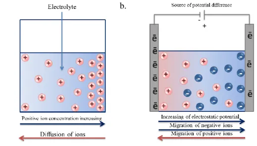
In a solution ions are moving under different applied forces to compensate their influence. This movement has two aspects: an individual aspect and a group aspect. The individual aspect takes in account an individual motion of every ion present in the solution; this ions movement is usually random in direction and speed. The group aspect is more significant because it account on the group ions movement in a certain direction producing the flux (or drift) of ions, this results not only directed transport of charges, but also transport of mass.
Ionic flux could have three different origins:
1) The difference in the concentration in different regions of electrolyte would result a concentration gradient, which produces a flow of ions to compensate the concentration difference. This type of flux is called diffusion (Figure 2.4a).
2) The difference in electrostatic potentials in different electrolyte regions would lead to flow of electric charges under the applied electric field - drift of charges (Figure 2.4b).
3) The gradient of temperature or pressure that gives rise to a flow of charges is called convection.
Despite of the origin, any flux is a result of the reaction of a system, that is distorted, that leads to an equilibrium maintaining.
20
a. b.
Figure 2.4 – Origins of ionic flux in electrolyte: a) Diffusion due to gradient of concentration; b) Migration due to gradient of potential
Diffusion is a movement of molecules to the region of lower concentration from the region of higher concentration. The diffusion in the steady state is proportional to the gradient of concentration. The diffusive flux relation with concentration is described by Fick’s law (here it is presented in one spatial dimension):
𝐽𝑑𝑖𝑓= −𝐷𝑑𝑐𝑖 𝑑𝑥
(2.12)
Where D is the diffusion coefficient.
The diffusion coefficient or diffusivity could be calculated using the Einstein–Smoluchowski relation[59]:
𝐷 =𝜇𝑖𝑘𝐵𝑇 𝑞
(2.13)
Where µi - the electrical mobility of charged particle; q - electrical charge of the particle
As soon as equilibrium is reached and there is no more gradient of concentration only process of self-diffusion, which originates from the random molecular motion, takes place in the solution. So-called dynamic equilibrium is established. The diffusion process and an absence of the other external forces will cause a complete and uniform mixing in the solution.
Under applied potential and created electric field ions are starting to compensate an electric field to restore equilibrium of the system. So negatively charged ions are starting to drift towards the higher potential (or more positive electrode immersed into solution); positively charged ions are moving towards an area with lowest potential (or negatively charged electrode). As a result the spatial separation of charges is produced, but electroneutrality of electrolyte is never the less preserved. The drift flux of ions could be described with the following formula (here in one spatial dimension):
𝐽𝑑𝑟𝑖𝑓𝑡= −𝜇𝑖𝑧𝑖𝑞𝑐𝑖
𝑑𝜑 𝑑𝑥
21 Since the drift of ions takes place due to the fact that they are charged, the flux of negative and positive ions could be separately presented as:
𝐽+ 𝑑𝑟𝑖𝑓𝑡= −𝜇𝑖+𝑧𝑖+𝑐𝑖+𝑞 𝑑𝜑 𝑑𝑥 (2.15) 𝐽− 𝑑𝑟𝑖𝑓𝑡= 𝜇𝑗−𝑧𝑗−𝑐𝑗−𝑞 𝑑𝜑 𝑑𝑥 (2.16)
The convective term is used to describe excitant gradient temperature or pressure in the solution. Combined together with the drift and diffusion terms the total ionic flux in electrolyte solution could be described. So the Nernst-Planck equation is obtained. Here this equation is represented in one-dimensional mass transfer form:
(2.17)
In general, in three-dimensions, the Nernst-Plank equation takes the following form:
𝐽𝑖 = −𝐷𝑖∇𝑐𝑖−𝑧𝑖𝐹𝑞
𝑅𝑇 𝐷𝑖𝑐𝑖∇𝜑 + 𝑐𝑖𝒗
(2.18)
In case of an unstirred or stagnant solution with no gradients of density last, convective term is suppressed:
𝐽𝑖= −𝐷𝑖∇𝑐𝑖−𝑧𝑖𝐹𝑞
𝑅𝑇 𝐷𝑖𝑐𝑖∇𝜑
(2.19)
In case of charged species, such as ions in electrolyte flux Ji, is equivalent to the current density.
This is how an ionic current in electrolyte is established.[60]
Ion-Electrode interaction in electrolyte solution
In an Organic Electrochemical Transistor the Gate electrode is put in contact, or immersed into an ionically conductive solution. Understanding of the processes that takes place at this interface is essential for understanding of the whole transistor working principle [13, 47, 61].
Electrode kinetics depends on electrode surface structure, purity and chemical reactions occur there. It is possible to classify all electrodes according to chemical process that happen in their interface in polarizable and non-polarizable electrodes[56].
Ideally polarizable electrode is characterized by absence of net reaction on its surface. That means that only transient (displacement) current could flow through its interface due to non-faradaic process. When potential is applied, charges will move towards an interface and accumulate there. Charging (displacement) current will flow to compensate for an excess (or deficiency) of the electrons in the interfacial electrode layer. Amount of this current will depend on the resistance in
22 the circuit. Basically, if there is no electrochemical reaction at the electrode it is possible to consider the electrode-solution interface as analogous to a capacitor, which capacitance C is proportional to stored charge q per applied potential E:
𝐶 = 𝑞 𝐸
(2.20)
The amount of charge at the metal electrode is equal to amount of charge in the solution. All the stored charges form electrical double layer which composed of different sub-layers:
1) Inner layer (Helmholtz layer or Stern layer) where stay molecules which are specifically absorbed (inner Helmholtz layer) and nearest approached solvated ions (outer Helmholtz layer) that are non-specifically absorbed due to electrostatic interaction with an electrode. 2) Outer layer (Diffuse layer) is composed of the rest of redistributed non-specifically adsorbed
ions. It is located between the Outer Helmholtz Plane and the bulk of electrolyte. Thickness of a diffuse layer is dependent on electrolyte concentration, for the small concentration it is about 100 Ǻ.
Figure 2.5 – The schematic representation of an electrolyte structure near an ideally polarizable electrode[62]
The presence of a diffuse double layer leads to the drop of potential near the electrode surface, so existence of a double layer mustn’t be neglected for an accurate description of processes in any electrochemical system.
An ideally non-polarizable electrode shows exactly the opposite type of behavior. Current is passing freely through a perfectly non-polarizable electrode, so this electrode is characterized by an interfacial reaction due to the presence of a faradaic process. If there is a more negative potential applied on the electrode, electrons are gaining higher energy that could be sufficient enough for an electron transfer from an electrode to ionic species adsorbed on the electrode. That means a reduction reaction takes place on the surface and reduction current flows through the electrode-electrolyte interface. An opposite - oxidation process could take place if an electrode potential is high enough, so for electrons of ionic species there is more favorable to flow from an electrolyte to an electrode, creating oxidation current. A critical potential at which these processes take place is related to the standard electrochemical potential E0[56]. The current is proportional to stoichiometric
23 process is proportional to amount of charge that passes through the electrode’s interface. The relationship between current (or charge that passes) and amount of product formed as a result of an electrochemical reaction could be calculated by using the Faraday’s law:
𝑚 =𝑄𝑀 𝐹𝑧
(2.21)
Where m - mass of the product as a result of an electrode reaction; M - molar mass of the product; Q - electric charge passes the boundary; F - Faraday constant
Even though the potential of an electrode is not enough to perform an electrochemical reaction other processes will, never the less, occur independently from the faradaic process at the interface. The processes called non-faradaic, such as an adsorption and desorption would influence on a solution-electrode interface. When potential is applied ions are migrating from the bulk to electrode surface region, where the chemical reactions could take place, then they are adsorbed on the electrode surface, where an electrochemical reaction with an electron transfer happens. External current could flow due to the adsorption - desorption process, even if there is no electrochemical reaction in the interface. Product desorbed after an electron transfer diffuses from an electrode surface to the bulk of the electrolyte under the gradient of concentration and the gradient of an electric field (in case if the product is charged). There are also possibilities of chemical reactions between the product and the other species in the electrolyte in the bulk or in the near-electrode region. (Figure 2.6)
Figure 2.6 – Schematic representation of the process near the non-polarizable electrode under applied potential[56]
As a result when there is a reaction at the electrode: both faradaic and non-faradaic processes take place; only non-faradaic process is possible in case of an absence of the reaction, but the transient current could still flow due to adsorption-desorption process. Charging current could be very significant in case of low concentration of an electrolyte. In some cases it could be even larger than faradaic current. To conclude: both faradaic and non-faradaic processes must be taking in account for the proper explanation of the reaction and charge transfer in a system.
Organic electronically conductive materials
Even though organic conductive materials in general have lower conductivity than inorganic semiconductors or conductors they have a lot of advantages in comparison with inorganic materials,
24 such as: low cost, easy properties tuning by chemical modification and a lot of fabrication possibilities by different techniques. Conductivity of organic conductors highly varies in the range 10-2 - 105 ohm-1cm-1, and depends on the type of organic conductor itself and also on its dopant.[63] Organic conductors could be categorized into conductive small molecules and conductive polymers. Small molecules are conductive materials that have the weight less than 1000 daltons, par contrary conductive polymers are defined by mass bigger than 1000 daltons. According to IUPAC definition polymer is a substance composed of macromolecules. Macromolecule is a molecule of high relative molecular mass, the structure of which essentially comprises the multiple repetitions of units derived, actually or conceptually, from molecules of low relative molecular mass.[64] In general small molecules are more soluble in organic solvents, but polymers have better mechanical properties and in general higher conductivity due to doping possibility.
Structure and conductivity of organic conductors
Even though the structure of conductive polymers and conductive small molecules is different, the source of conductivity has the same chemical and physical nature. To understand the nature of organic material conductance it is necessary to look precisely at the chemical structure and bonds’ configuration of these molecules.
The core element of an organic conductive material is carbon which has a 1s22s22p2 electron configuration. Core orbital electrons are not participating in a chemical bonding, so in covalent bond formation only four electrons from 2s22p2 take part. While bonding with other atoms depending on the number of combined orbitals, formation of orbitals with different type of hybridization: sp1, sp2, sp3 is also possible. (Figure 2.7) As a result single, double or triple bonds are formed.
methane CH4 ethylene (ethane) C2H4 acetylene (ethyne) C2H2
Figure 2.7 – Different types of carbon bond hybridizations and example of organic molecules with this hybridization type[65]
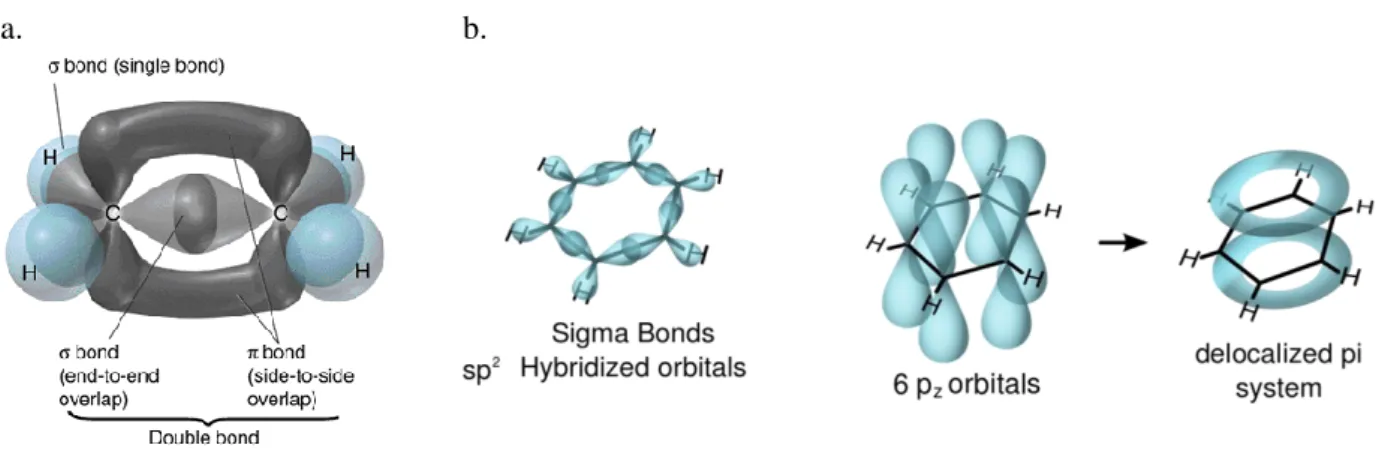
Conducting properties of a polymer is closely related to its chains and bonds configurations. To be conductive, organic material should have a chain with sp22pz hybridization. In conductive
materials one 2s orbital pairs with two 2p orbitals of a carbon atom to form 3 sp2 orbitals. Two out of three sp2 orbitals form covalent bonds with neighboring carbon atoms and the last sp2 orbital forms a covalent bond with the side group, or with a hydrogen atom. This type of bond is the
25 strongest type of a covalent bond which is formed by head-on overlapping of the atomic orbital (Figure 2.8), it is called σ-bond.[66, 67] The left pz orbital of a carbon atom overlaps with pz orbital
of a neighbored carbon atom and forms π bond. This type of bond is weaker than σ-bond, so it has much less energy and less stability due to smaller overlap between two pz orbitals.
a. b.
Figure 2.8 – Formation of σ and π bonds in: a) ethylene molecule; b) benzene molecule
Bonding weakly, the electrons of a π bond are easily delocalized. Split of π bond on π bonding and π*
anti-bonding band leads to the energy-gap (Eg) formation. Conjugated molecules are the
molecules that have single and double bonds alternation. The increase of the number of double bonds in a conjugated molecule leads to an energy-gap decrease. In case of large number of interacting pz orbitals – fully occupied π-valence bond and empty π*-valence bond are formed. In
this case energy gap is determined as the difference between lowest unoccupied molecular orbital (in conduction band)-LUMO and highest occupied molecular orbital (in valence band) - HOMO (Figure 2.9).[68]
Figure 2.9 – Energy band formation in conjugated polymer materials[69]
The Band gap determines conductive properties of the material; it depends on molecule structure and the number of repeating units, so this property could be tuned on molecular level by changing the molecular structure of a material.
Conductive properties of organic materials are in a lot of cases highly dependent on additives that could tune conductive properties towards much higher or lower values.
26
Doping of conductive materials
The most widely used class of organic conducting materials is conductive polymers. Piscine π-conjugated polymers don’t have very high conductivity; this characteristic could be increased trough the doping process. There exist n-type and p-type dopants. The conductivity of a material is proportional to a doping concentration up to some extent, but even a small amount of dopant (several ppm) could increase sufficiently the conductivity of a conjugated polymer. Dopant is charge-transfer agent used to generate, by oxidation or reduction, positive or negative charges in an intrinsically conducting polymer[4]. In conductive polymers dopant molecules are placed between conjugated polymeric chains, it doesn’t form with them covalent bonds, but attached to them by Coulomb force (Figure 2.10) [70]. Addition of a dopant forms an ionic complex with a conjugated polymer by an electron exchange and provokes a charge separation near the polymer molecule keeping, never the less, the global electroneutrality.
Figure 2.10 – Process of n-type doping of polymer molecule[71]
Chains of the conjugated polymer are starting to deform immediately after doping. The charge is delocalized along several units of the polymeric chain, the difference between single and double bonds decreases gradually, it causes a polaron creation. There are two types of polarons: P+ (hole) polaron - electron from lower polaron level leaves and going to an accepter; P- (electron) polaron- electron is leaving donor and goes to the accepter higher level. In terms of chemistry polaron is lattice distortion associated radical ion.[72] Formation of polaron and bi-polarons (lattice distortion associated union of two like charges) is possible in doped conjugated polymers. Polarons are formed in case of low doping level and bi-polarons are formed in case of higher doping level.
Charge transport in conductive polymers is a multi-scale process. In an intra-molecular level under applied potential bi-polaron or polaron travels along the chain causing charge propagation with continuous polymer conformational changes[63]. Electron or hole current could be defined depends on polaron origin. Charge hopping process occurs between two macromolecular chains in the inter-molecular level. In supra-molecular level charge travels by a percolation between amorphous and crystalline domains (Figure 2.11).
27 Figure 2.11 – Schematic representation of multi-scale transport in conductive polymers[73]
All three scales of charge transport are affecting the total charge transport process, so parameters such as molecular chain flexibility and structure, packaging and aggregation should be considered during synthesis and processing of the material[73].
Charge carrier transport in conductive polymers
Conductive polymers could be doped by one of two different types of dopant: n or p-type. As a result depending on dopant type one of two polarons is created: p+- polaron and n-- type polaron. So the main charge carriers in conductive polymers are electrons and holes. The set of equations governing electrons and holes transport in conductive polymers is very similar to those one that is used for positive and negative ions transport description in electrolyte. So holes and electrons density distribution and movement is described by the set of Drift-Diffusion and Poisson-Boltzmann equations:
∇ ∙ 𝜀∇𝜑 = −𝑒(𝑝 − 𝑛) (2.22)
𝑱𝑝= 𝑒𝜇𝑝𝑝𝑬 + 𝑞𝐷𝑝∇𝑝 (2.23)
𝑱𝑛= 𝑒𝜇𝑛𝑛𝑬 + 𝑞𝐷𝑛∇𝑛 (2.24)
Where p and n – holes’ and electrons’ concentrations, µp and µn -holes’ and electrons’ mobility,
Dp and Dn -holes’ and electrons’ diffusion constant.
Similar to an ionic case, this set of equations has an analytical solution only in limited amount of very particular cases, so the proper solution could be obtained only in case of a numerical model building.
PEDOT:PSS as an electronic conductor
The main interest of this thesis is an Organic Electrochemical Transistor, in particular OECT with poly(3,4-ethylenedioxythiophene) polystyrene sulfonate (PEDOT:PSS) as electron-conductive layer. PEDOT:PSS has a good biocompatibility, thermal, electrical and electrochemical stability.[74] A relatively high conductivity, about 1000 S·cm-1
allows to fabricate not only conductive channel, but also Source, Drain and Gate electrodes from PEDOT:PSS[75].
From a chemical structure point of view, PEDOT:PSS is a mixture of polytheophene polymer (PEDOT) doped by polystyrene sulfonate (PSS) polyanion (Figure 2.12). PEDOT:PSS is a heavily
28 doped p-type conductive polymer, in which PSS- compensates a positive charge from PEDOT backbone that creates a positive polaron redistributed through several polymeric units and forms a poly-ion complex[76].
Figure 2.12 – Chemical structure of PEDOT :PSS p-type conductive polymer (modified from[77])
PEDOT:PSS complex exists in water in a form of colloidal gel particle, which could be processed into a fiber, thin or thick film by the variety of techniques, such as spin-coating, inkjet printing, flexography, lithography[76].
PEDOT:PSS is usually synthesized from EDOT monomer and PSS in water phase with an oxidizing agent – sodium peroxodisulfate. PEDOT itself is not soluble in any solvent, but PEDOT in oligomeric form (about 20 units) in ionic complex with PSS is dispersed in an aqueous medium. The ratio of PEDOT:PSS which is normally used for organic electrochemical transistors fabrication is 1:2.5 with amount of water equal to 2%. A dispersion contains 1-2.5% PEDOT:PSS in water has an optimal viscosity to be used by main deposition techniques[76]. Different dispersions of PEDOT:PSS are commercially available by Clevios and Sigma Aldrich. To better crosslink PEDOT:PSS film, for more stable operation in an aqueous environment, (3-glycidyloxypropyl) trimethoxysilane (GOPS) is often added[78]. It is possible to enhance the conductivity of a PEDOT:PSS layer by different additives integration during film formation. For example, ethylene glycol (EG) addition increases both an inter- and intraparticle charge carrier transport.[79] The addition of 3% EG would lead to an increase of PEDOT:PSS conductivity up to two orders of magnitude (from 3 S cm-1 to 175 S cm-1), but further increase of ethylene glycol concentration would lead to conductivity decrease. The possible explanation of this effect could be that in a pristine film PEDOT:PSS has the structure of aggregates of an amorphous PEDOT surrounded by an insulating PSS (Figure 2.12d) where the transport is unfavorable due to relatively high activation
29 energy (about 20 meV). An addition of a small amount of EG would promote the PEDOT phase crystallization and the insulating PSS shell thickness decrease, which lowers an activation barrier to 5.1 meV and promotes a charge-carrier hopping. Further increase of EG concentration would lead to increase of conductive domains size and defects formation[77]. Further enhancement of conductivity is also possible by different methods, for example by a solvent addition[80, 81] or a thermal treatment [82].
One of important and remarkable properties of PEDOT:PSS is it’s electrochromic behavior. Electrochromism is a property of a material to reversibly change the color as a result of changing the state due to redox reaction[83]. In case of PEDOT:PSS the color is switching from light-violet (near-infrared) to deep blue (visible). Figure 2.13 represents an absorption spectrum of PEDOT:PSS. It could be seen that upon application of the potential the absorption spectrum has been shifted towards lower waive-length.
Figure 2.13 – Absorption spectrum of PEDOT:PSS in OECT at 0V and 1V of applied Gate potential[84]
This kind of behavior could be explained as a result of following redox reaction[85]:
𝑃𝐸𝐷𝑂𝑇++ 𝑒−↔ 𝑃𝐸𝐷𝑂𝑇0 (2.25)
The potential difference change of the system leads to a change of the system’s free energy. Thus this potential change is linked with all sorts of electrochemical change, such as electrochemical reactions that take place in the system.
If the reversible redox reaction takes place in the system (such as it is PEDOT+↔ PEDOT0), than the Nernst equation is used to describe the dependence of the reagent-product concentration from electrochemical potential[86]. It is worth mentioning that the Nernst equation is only used to treat a thermodynamically and electrochemically reversible system in the equilibrium state, which means when rates of a reduction reaction and an oxidation reaction are equal.
If the reaction in the system could be described by the following equation:
𝑂𝑥++ 𝑒−↔ 𝑅𝑒𝑑0 (2.26)
Where Ox+ is the concentration of oxidized (reagent) species; Red0 – concentration of reduced (product) species, then the concentration-potential dependence could be calculated from the following Nernst equation of half-reaction:
30 𝐸 = 𝐸0+𝑅𝑇 𝑛𝐹𝑙𝑛 𝑎𝑂𝑥 𝑎𝑅𝑒𝑑 (2.27)
Where αOx and αRed are activities of oxidized and reduced species.
For low concentrations it is possible to use the concentrations of reduced and oxidized species instead of activities: 𝐸 = 𝐸0+𝑅𝑇 𝑛𝐹𝑙𝑛 𝐶𝑂𝑥 𝐶𝑅𝑒𝑑 (2.28)
Where COx and CRed are the concentrations of an oxidized and a reduced species; R - standard gas
constant; T - temperature; n - number of transferred electrons; E0-standard potential of the reaction.
Using this equation it is possible to calculate the concentration of a reagent:
𝐶𝑂𝑥= 𝐶𝑅𝑒𝑑 𝑒𝑛𝐹(𝐸−𝐸 0) 𝑅𝑇 (2.29) 𝐶𝑂𝑥= 𝐶𝑅𝑒𝑑𝑒𝑛𝐹(𝐸 0−𝐸) 𝑅𝑇 (2.30)
From this representation of the Nernst equation it could be easily seen that under equilibrium, concentration of the reactant (COx) is proportional to concentration of the product and reversely
proportional to the temperature of the system and highly dependent on applied potential: if applied potential is higher than standard potential of reaction, then equilibrium is shifted towards the higher concentration of the product and vice-versa[56].
According to the Figures 2.14a and 2.14c, the reduction potential for PEDOT:PSS molecules from three different producers is from 0V to -0.1V and oxidation potential is about 0.1-0.2 V[83]. As soon as the applied potential is greater than reduction potential of PEDOT+, the reduction reaction takes place and PEDOT+ is transferred to PEDOT0. The result of a redox reaction of the real PEDOT:PSS is shown on Figure 2.14b.
31
a. b.
c.
Figure 2.14 – Redox behavior of PEDOT:PSS: a) Theoretical cyclic voltammogram; b) Electrochromic PEDOT:PSS behavior as a result of redox reaction[87] ;c) Cyclic voltammogram of PEDOT:PSS [88]
An electrochromic behavior of PEDOT:PSS is interesting not only from its application point of view. Being a wonderful tool to track ions, PEDOT+ distribution and device conductivity profile it also helps to understand the dedoping process that happens upon the application of certain gate potential in Organic Electrochemical Transistors.
OECT modeling
There are two different approaches to a device modeling: numerical and analytical. The purpose of both types of models is a correct description and prediction of the main characteristics of a modeled object and processes occurring inside modeled object under known applied conditions. An analytical model normally allows calculating precisely the main characteristics of an investigated object and obtaining the exact solution. A numerical modeling is used when parameters and all device characteristics couldn’t be calculated analytically. Numerical models do not give an exact solution of solved equations; instead, the solution with a certain degree of approximation is the result of numerical calculations. Never the less, both types of models are important for understanding the device physics and chemistry. To build up a working model it is useful to study precisely the already excising state of the art.
There exist several analytical models of an OECT that could give, up to some extent, an explanation and prediction of the device properties. Most of the models are considering depletion mode of an OECT operation. Different behavior of Organic Electrochemical Transistors is well defined for transient and steady-state. These models could be differentiated one from another taking in account to which state of operation a model is dedicated. A lot of models are looking at an
![Figure 1.2 – Architecture of OFET and OECT transistors. Sensing part, that could be also functionalized, is marked by red[8]](https://thumb-eu.123doks.com/thumbv2/123doknet/2969238.82385/11.892.190.731.552.933/figure-architecture-ofet-oect-transistors-sensing-functionalized-marked.webp)
![Table 1.1- Bio-analytes that could be detected by different biosensors (modified from [33])](https://thumb-eu.123doks.com/thumbv2/123doknet/2969238.82385/12.892.223.666.700.1081/table-bio-analytes-detected-different-biosensors-modified.webp)
![Figure 1.4 – Schematic representation of different types of OFET transistors: a) Typical EGOFET biosensor; d) Typical OECT biosensor (modified from [38])](https://thumb-eu.123doks.com/thumbv2/123doknet/2969238.82385/13.892.124.768.847.1033/schematic-representation-different-transistors-typical-biosensor-typical-biosensor.webp)
![Figure 2.1 – Solvation process in aqueous electrolyte solution: a) Water molecule interaction with NaCl salt crystal; b) Formation ion of surrounding hydration shells [54]](https://thumb-eu.123doks.com/thumbv2/123doknet/2969238.82385/18.892.104.780.181.473/solvation-electrolyte-solution-molecule-interaction-formation-surrounding-hydration.webp)
![Figure 2.5 – The schematic representation of an electrolyte structure near an ideally polarizable electrode[62]](https://thumb-eu.123doks.com/thumbv2/123doknet/2969238.82385/24.892.271.638.458.731/figure-schematic-representation-electrolyte-structure-ideally-polarizable-electrode.webp)
![Figure 2.6 – Schematic representation of the process near the non-polarizable electrode under applied potential[56]](https://thumb-eu.123doks.com/thumbv2/123doknet/2969238.82385/25.892.211.707.580.811/figure-schematic-representation-process-polarizable-electrode-applied-potential.webp)
![Figure 2.7 – Different types of carbon bond hybridizations and example of organic molecules with this hybridization type[65]](https://thumb-eu.123doks.com/thumbv2/123doknet/2969238.82385/26.892.105.773.676.944/figure-different-carbon-hybridizations-example-organic-molecules-hybridization.webp)
![Figure 2.13 – Absorption spectrum of PEDOT:PSS in OECT at 0V and 1V of applied Gate potential[84]](https://thumb-eu.123doks.com/thumbv2/123doknet/2969238.82385/31.892.239.671.370.635/figure-absorption-spectrum-pedot-oect-applied-gate-potential.webp)