UNIVERSITE DE SHERBROOKE
Faculte des sciences appliqueesDepartement de genie electrique et de genie informatique
LINEARISATION NUMERIQUE ET ANNULATION DU
COUPLAGE CAPACITIF POUR
UN MICROSCOPE A EFFET TUNNEL
par
RAN TANG
Memoire de maTtrise
Octobre 1997
Linearisation Numerique et Annulation du Couplage Capacitif
pour un Microscope a Effet Tunnel
RESUME
Cette these decrit Ie developpement et Ie test d'un systeme de controle numerique, controlant la distance pointe-echantillon (largeur de gap) pour un microscope a effet
tunnel.
D y a deux difficultes normalement associees avec les controleurs analogiques traditionnels dans de tels microscopes. La premiere est la relation exponentielle entre la largeur de gap et Ie courant tunnel. La deuxieme est Ie bmit introduit dans la boucle de contr61e, et sur 1'image balayee, par Ie couplage capacitif entre la pointe et les electrodes des piezo-moteurs qui la deplacent.
Le controleur numerique con^u resoud chacun de ces problemes. D produit une linearisation du comportement de la jonction tunnel independante de la frequence en introduisant une fonction logarithmique dans la boucle de controle numerique. De plus, la fonction de transfert des effets du couplage capacitif de 1'axe vertical est modelisee gr^ce a un filtre adaptatif utilisant 1'algorithme LMS (Least Mean Square). Ce modele est alors reutilise dans Ie domaine numerique pour annuler les effets du couplage capacitif.
Les benefices supplementaires d'un systeme de controle entierement numerique sont:
• Un ajustement facile, de grande precision, et pouvant etre effectue en simulation, des parametres de controle.
• Une plus grande stabilite thermique et dans Ie temps des parametres de controle qu'avec un systeme analogique.
• Une calibration dynamique facile de la tension continue de decalage du
courant detecte.
• Une automatisation facile de 1'instmment.
• Puisque la boucle de controle opere deja entierement dans Ie domaine numerique, aucune autre conversion n'est requise, eliminant ainsi la necessite de plusieurs circuits de conversion analogique/numerique.
Dans Ie systeme decrit, la boucle de controle est realisee sur une carte de traitement de signal numerique (DSP) point fixe TMS320C50 peu couteuse. Le taux d'echantillonnage est de 25 KHz. Les simulations et les resultats pratiques sont presentes.
Digital Linearization and Capacitive Coupling Cancellation for
a Scanning Tunneling Microscope
ABSTRACT
The development and test of a DSP-based digital control loop to control the tip-to-specimen distance in a Scanning Tunneling Microscope are described in this thesis.
There are two difficulties normally associated with traditional analog controllers: One is the exponential relationship between the tip-to-specimen distance and the tunnel current, the other is the capacitive coupling between the electrodes of the scan tube and the input of the current-to-voltage converter, which induces noise in the control loop as well as in the scanning image.
The digital controller we designed tackles both problems. It provides a
frequency-independent linearization of the tunnel junction by inserting a digital logarithm function
in the control loop; A precise cancellation of the capacitive coupling in the Z direction is also achieved by first identifying its transfer function using a LMS adaptive filter, then compensating its effect in the digital domain using the identified model.
Added benefits of the completely digital control system are:
• Easy adjustment of the control parameters through simulation with great precision, decreasing the possibility of crashing the tip to the specimen.
• Stable control parameters not likely to drift with time or temperature. • Easy on-line calibration of the current detection offset bias.
• Easy automation of the instrument.
• No need of additional digitizing electronics, since the control loop already does the digitization, and operates in the digital domain.
In the described system, the control loop is implemented on an inexpensive fixed-point
DSP TMS320C50 board. The sampling rate could reach 25 KHz. Simulations and
ACKNOWLEDGEMENT
I wish to express my sincere gratitude to all those who advised and helped me throughout this research, especially to Professor Bruno Paillard, my research supervisor, who, despite his numerous tasks, not only has constantly found time to provide his valuable guidance and encouragement during the time I carried out this research, but also has spent a great deal of time and energy to test the control system in the real STM and offered me all the practical results, which makes the content of this thesis much more significant and substantial. His generous help always makes me feel confident in overcoming the difficulties in both research and personal life.
Also, I gratefully acknowledge the help of Professor Paul Rowntree, who has directed the experiment and let us play with his delicate equipment STM with precious confidence. Without his support, the whole research work couldn't have progressed so smoothly and successfully.
Many others have assisted in different ways in the completion of this thesis. I would like to thank all the faculty members in Departement de genie electrique et de genie Informatique, Universite de Sherbrooke, for their kindness and helpful encouragement.
Finally, thanks to my husband, Runbo Fu, for his limitless concern and support in the last
two years.
CONTENT
RESUME ...i
ABSTRACT ...iii
ACKNOWLEGEMENT ...v
CONTENT ...vi
LIST OF FIGURES ...viii
INTRODUCTION ...1
STATE OF THE ART ...5
2.1 Principle of STM ...5
2.2 History of STM Development ...6
SYSTEM DESCRIPTION ...11
3.1 Hardware ...13
3.1.1 Digital Control Board...13
3.1.2 STM Emulation ...18
3.2 Software ...20
LOGARITHM CONTROL...24
4.1 Linearization of the Tunnel Junction ...25
4.1.1 Digital Implementation of the Logarithm Function ...26
4.1.2 Problems Due to the Input Offset Bias ...30
4.1.3 Problems Due to the Rectifier...31
4.2 PICorrector ...32
CAPACITIVE COUPLING COMPENSATION ...35
5.1 Problem and Symptoms ...37
5.3 Compensation Procedure and Results.. ...43
6 PARAMETER ADJUSTMENT ...49
6.1 Open Loop Identification ...50
6.2 Closed Loop Prediction ...53
6.3 Complete Adjustment Procedure ...54
7 RESULTS ...56
7.1 Adjustment Strategy ... ..56
7.1.1 STM Emulator ...56
7.1.2 Real STM ...58
7.2 Effect of the Logarithm Function ...60
7.3 Effect of the Capacitive Coupling Compensation ...62
7.4 Scanning Lnage ...63
8 CONCLUSION ...65
APPENDICES ...66
A: List of Symbols and Abbreviations ...66
B: Code of the logarithm function ...68
REFERENCES ...69
LIST OF FIGURES
Figure 1.1 Block diagram of the STM and its control loop ...2
Figure 3.1 STM and the digital control loop ...12
Figure 3.2 Block diagram of the DSKX board architecture ...14
Figure 3.3 Block diagram of the electronic emulator ...18
Figure 3.4 Impulse response of the z capacitive coupling of the emulator ...19
Figure 3.5 Transfer function of the z capacitive coupling of the emulator ... 19
Figure 3.6 Exponential input/output relationship of the emulator ...20
Figure 3.7 Architecture of the software running on the PC ...21
Figure 3.8 STM main control panel designed using Lab VIEW ...22
Figure 3.9 Architecture of the code running on the DSK board ...23
Figure 4.1 Block diagram of the STM digital control loop ... ..24
Figure 4.2 Digital logarithm function result ...28
Figure 4.3 Computation error of the digital logarithm function ... ..28
Figure 4.4 Exponential function of the STM emulator linearized by a computed logarithm function ...29
Figure 5.1 Block diagram of the capacitive coupling between the electrodes of the piezo-actuators and the input of the current-to-voltage converter .. ...36
Figure 5.2 System identification based on FIR model and LMS algorithm .... ...40
Figure.5.3 Compensation of the capacitive coupling from the Z piezo-motor ... ....44
Figure 5.4 Prediction error and desired output signal of LMS adaptive filter ... ....45
Figure 5.5 Zoom of the error signal in the above graph ... ....45
Figure 5.6 64-sample identified impulse response of the Z capacitive coupling for the real STM ...46
Figure 5.7 Transfer function of the Z capacitive coupling for the real STM ... ....46
Figure 5.8 Detection of the compensation result with a white noise to the capacitive coupling emulator ...47
Figure 5.9 Zoom of figure 5.8 ...47
Figure 6.2 Simulation of the open loop STM from the closed loop identified
response ...51
Figure 6.3 Perturbation closed loop response ...53
Figure 7.1 Closed loop step response of the STM emulator with a very small
integral gain ...57 Figure 7.2 Open loop impulse response of the STM emulator, derived from
the closed loop step response ...57
Figure 7.3 Perturbation step response of the STM emulator, with optimized
coefficients ...58 Figure 7.4 Zoom on figure 7.3 ...58
Figure 7.5 Closed loop step response of the real STM with very small integral
and proportional gains ...59
Figure 7.6 Open loop impulse response of the real STM derived from the closed
loop step response ...59
Figure 7.7 Perturbation step response of the STM with optimized coefficients ...60
Figure 7.8 Zoom on figure 7.7 ...60
Figure 7.9 Closed loop Perturbation Step Response for three values
of the set-point ...61 Figure 7.10 Zoom on figure 7.9 ...61
Figure.7.11 Perturbation Step Response with the proper capacitive coupling
compensation ...62 Figure 7.12 Zoom on figure 7.11 ...63
Figure 7.13 Perturbation Step Response with no capacitive coupling compensation. The simulated response assumes a proper compensation and is
equivalent to figure 7.11 ...63
Figure 7.14 Topography image obtained using our STM control system ...64
Chapter 1. INTRODUCTION
The Scanning Tunneling Microscope (STM) invented by Binning and Rohrer in 1982 has
become an important instmment in surface science laboratories due to its capability to obtain atomic resolution.[1] The STM utilizes the high sensitivity of tunnel current flowing through the gap fanned between the tip and the sample. By controlling this current and scanning the tip over the surface of the sample, the topography of the surface or measurement of some electronic properties of the sample is obtained with atomic
resolution.
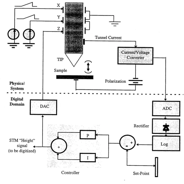
During STM operation, a sharp tip is scanned over the sample. The displacement of the tip is controlled by piezo-electric actuators in three directions, X, Y, and Z. While the tip is maintained very close to the sample, a tunnel current can be detected between them. The current depends exponentially on the tip-to-specimen distance. A feedback control loop is applied to maintain a constant current, i.e. constant tip-to-specimen distance. Thus, by scanning the tip in raster manner and mapping the correction voltage required for the Z piezo-motor to maintain the current constant at each X-Y raster point, a "picture" of the atomic topography may be obtained.
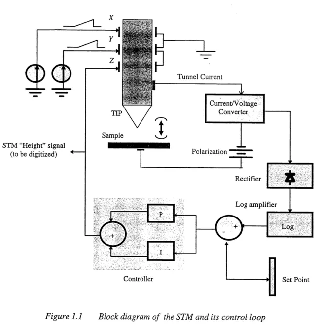
Figure 1.1 shows the block diagram of a typical analog control loop.
The design of the control loop presents two difficulties:
• The relationship between the tip-to-specimen distance and the tunnel current is exponential, while the actuation function, i.e. the relationship between the voltage on the Z piezo-mbtor and the distance between the tip and the specimen, is linear. This requires the control loop to be linearized, or to be operated in a small range around a well controlled operating point.
STM "Height" signal (to be digitized) Sample
t
Cun-enfc^Voltage Converter Polarization .X:P.:'\, .,,J.:. ••\';'\Controller Set Point
Figure 1.1 Block diagram of the STM and its control loop
The tunnel current detected is very small. Capacitive coupling between the electrodes of the piezo-motors and the stylus induces stray current into the input of the current-to-voltage converter. Even if the value of the stray capacitance is only a few fractions of pF, this current can be on the same scale as the tunnel current being detected. This affects the performance of the control loop and introduces noise in the image.
The work described here tackles both problems by a DSP (digital signal processor) based digital control approach. For the first problem, we insert a digital logarithm function in the feedback loop to linearize the exponential function between the tip-to-specimen distance and the tunnel current. As for the second problem, we first identify the transfer function of the capacitive coupling by using a LMS ( least mean square) adaptive filter, then model it in the digital domain to cancel its effect with high precision. Also, we will describe the optimization procedure for the parameters of the control loop which takes advantage of the fact that the controller is digital.
The objective of this work was only to design a feasible digital feedback control loop to control the tip displacement in the Z direction, and not to build a complete STM. So all the other important functions of a STM, such as scanning signals generation, data acquisition and display, image processing, etc., were kept as they were with the already existing analog control loop. The current microscope that we use as a testbed for our control strategy has been built by Professor Paul Rowntree. It features an analog control loop, a digital user interface, and the raster signals generation through the use of a PC and analog I/O boards.
Notice that in our digital control loop, we only considered the capacitive coupling compensation existing in the Z direction, instead of considering all the three directions, which always exist in practice.
The next step of the project is to design a more advanced digital control loop, with the necessary hardware and software support; it would not only consider all the capacitive coupling effects in three directions, but also enable us to achieve a complete automation of calibration and measurement procedure.
The next chapter of this thesis is devoted to the principle of STM and its evolution. Chapter 3 describes the basic hardware and software used in our system for STM control. Chapter 4 presents the achievement of the logarithm control, including the digital log
function and PI controller. The capacitive coupling identification and compensation will be presented in chapter 5. We will discuss a fine and precise control parameter optimization strategy in chapter 6. Finally, computer simulations and some practical results obtained with our system are going to be presented in chapter 7.
Chapter 2. STATE OF THE ART
2.1 Principle of STM
The operation of a STM requires a fine stylus to be kept at a small distance (5 to 10 A)
above the surface of a specimen to be imaged. As the atomically sharp conducting tip of the stylus reaches the electron cloud of the specimen, a small quantum tunnel current (~ 1 nA) is detected between the tip and the specimen. The tunnel current increases exponendally as the distance between stylus and specimen is decreased.
The 'position of the stylus is controlled by piezo-electric actuators in three axes. For our STM, the actuators take the form of a "scan tube", made with 4 sections of piezo-electric
ceramic (PZT), at the tip of which resides the stylus. By applying voltages to the
electrodes to selectively contract or expand each of these sections, a displacement in the X, Y or Z direction can be achieved.
To record an image of M. x M points, the tip position must be stepped across the surface in a raster pattern. For example, the tip is stepped from left to right M. times. At each step, the tunnel current must be read, and the tip height is adjusted to achieve the desired tunnel current. When the left-to-right scan is finished, the tip is returned to the left side of the scan area. The position of the tip is then moved one step in the Y direction, and the raster from left to right is repeated. This is done M times. When this is finished, an M x M array of Z positions has been recorded and this array is a surface image of the sample.
In the constant-current mode of operation, a control loop is used to keep the tunnel current at a constant value. As shown in figure 1.1, when the distance between the tip and the sample surface varies due to any system perturbation, the tunnel current also changes. Then the feedback control system compares a setup reference with a value given by the real system. The error value between them, which is a signal proportional to the tunnel
current, is used to generate a control signal to be applied to the Z piezo-actuator. By constantly adjusting the height of the stylus above the surface of the specimen, the tunnel current is kept at a constant value. By keeping the current constant, the controller keeps the gap between the stylus and the specimen constant. As the stylus scans the specimen along the X and Y axes, the output of the control loop is recorded. This yields an image of the height of the specimen.
As it is shown in the figure 1.1, since the tunnel current has an exponential dependence on the tip-to-specimen distance, to linearize the tunnel junction, it is common to use a logarithmic amplifier so as to avoid the difficulties associated with achieving stability in nonlinear systems, as well as to make the open loop gain independent of the steady state tunnel current. Due to the demand of choosing a positive or negative polarization of the specimen in most STM implementations, a rectifier is inserted just before the logarithmic amplifier to provide its required positive input. The tunnel current is detected in the tunnel junction by using a current-to-voltage converter and its output is sent to the logarithmic amplifier for linearization.
The controller for this application is usually a simple Proportional (P) Integral (I)
corrector. The Derivative (D) corrector is rarely used because of its noisy characteristics. By comparing the output of the Log amplifier with the desired set-point, the error signal is obtained as the input of the controller. The controller has a zero steady state error due to the presence of the integrator in the loop. It must be adjusted to give a stable closed loop behaviour, as well as a fast transient behaviour.
2.2 History of STM Development
Scanning Tunneling Microscopy (STM) has experienced a short but rapid development since the 1980s. It is based on the tunneling of electrons between a sharp tip and a conducting surface.1101 The concept of the electron tunneling is simple, but the
construction of a practical scanning tunneling microscope proved to be difficult because of the problems associated with maintaining the gap between the tip and the specimen. These problems were overcome by Binnig et al. at IBM Zurich in the early 1980s and led
to the rapid development of the STM and the award of the 1986 Nobel prize in physics.[ ]
In recent years, STM instmmentation has been refined to the stage where systems are essentially automatic and are increasingly "user-friendly". The control electronics can be considered as two logically discrete units: the feedback unit and the scanner unit. The feedback unit controls the Z movement of the tip, and the scanner unit controls its X - Y motion. The key component of controlling any STM is the computer system.[3][ ]
In the first generation of the STM control systems, both units were independent and "free-running",[ ] i.e. after initially selecting the scan parameters, the user had no control over them. They used little or no computer control, displaying raw STM data on storage oscilloscopes or chart recorders. Even if computers were used,[] they just functioned simply as chart recorder replacements. The tunneling tip was rastered parallel to the plane of the sample surface, in the X and Y directions, using piezoelectric scanners driven by voltages derived from a triangle-wave generator. Control of the distance between the tip and the specimen, in the Z direction, was performed by an analog feedback circuit.
In the second generation systems, the scanning was effected by a controlling computer while the feedback unit was still free-mnning and implemented by analog electronics.[] As better and faster computer systems were implemented, it became possible to replace the triangle-wave generators with digital-to-analog converters (DAC). Thus, a computer was able to control the raster motion in the X and Y directions. One example is a computer automation system for STM developed by Schroer et al. in 1986,[4] They designed a comprehensive data acquisition and image processing IBM PC/AT workstation to complement the STM. The computer was used to control the raster scans, to acquire multi-channel analog data, and to store data for later analysis both at the workstation and on a host computer. However, In most STM systems of the second
generation, control of the position of the tunneling tip in the Z direction was still largely accomplished with an analog circuit.
Modem, commercially available STM data acquisition and control systems are entirely computer controlled, and contain sophisticated image processing and display capability.[7] This is the third generation of STM control systems. Developing the feedback loop in software to replace the digital electronics allows the user greater control over the whole system. In particular, the feedback loop parameters are easily controllable by the host computer either from the keyboard or automatically by the STM control program. Furthermore, feedback functions implemented in software are inherently more flexible than hardware circuits. Feedback response functions more sophisticated than simple integration can be readily synthesized.
Computer control also allows greater flexibility in experiments done with a STM. For example, the measurement of the tunnel current as a function of distance between sample and tip can be easily performed if the Z position is under software control. Another example is the measurement of current as a function of tip voltage. In general, an analog feedback circuit will prove cumbersome for any STM application where either the tunnel current or the tip-to-specimen distance does not remain fixed during an experiment. In order to perform such experiments with analog circuits, the circuit must be especially designed to implement the experiment. For instance, either of the two examples mentioned above would require modifications, such as the introduction of sample-and-hold circuits to a standard analog Z feedback loop. Such modifications can be extensive and further increase the complexity of the Z feedback circuit.
A digital feedback loop system has already been reported by Finer et al.[} Their computer system controlled directly the tunnel barrier width, allowed STM scans to be performed at a speed which was automatically determined by the roughness of the surface under study. The system was based on a Motorola 68020 with a 68881 coprocessor. However, since the 68020 is a general purpose central processor unit (CPU), it is not
designed for high speed data processing and there is a "bottle-neck" in the data bus stmcture. Furthermore, the speed of the CPU is not fast enough to allow sophisticated scanning and feedback algorithms to be implemented.
Recently, increased DSP computing power has enabled us to build more straightforward digital control algorithms with far less cost. The major advantages offered by DSP-based control systems include greater flexibility in the choice of the signal processing algorithm, improved performance (decreased scan time, increased noise immunity, etc.), and greater ease of adjustment of loop parameters by the host computer. The tremendous flexibility of a DSP-based system arises from the generic nature of the analog I/O electronics combined with the ability to modify the control software. This allows the implementation of the novel imaging modes or the adaptation of the system to control different devices with a minimum of hardware development thus saving both time and expense. Another advantage lies in the capabilities of the DSP itself. Because DSPs typically contain features such as single machine cycle multiplication and matrix manipulation facilities, they are particularly well suited to real-time computation and signal processing. They are much faster for these tasks than micro-controllers or other
microprocessors.
An application example of DSP technology for the implementation of the feedback control loop of a STM was discussed by Morgan et al.w The system utilized a commercially available PC AT-compatible plug-in card based on the Texas Instruments TMS320 series of digital processing chip to implement a loop controller of PED type. Because of the exponential dependence of tunneling current on tip-to-specimen distance, they also employed a look-up table to emulate the logarithmic amplifier in the STM feedback loop. However, they only provided a general guidance in the construction of digital loop filters for STM application, no practical results were presented.
Another more detailed STM digital feedback control system using TMS320C30 floating
developed algorithm for self-optimizing PID feedback, raster generation (with hysteresis
correction, sample tilt compensation, and scan rotation), lock-in detection, and automatic tip-sample approach, etc. And some practical automatic optimization results were presented. But it seemed that with their system, STM generally produced poor step response curves for optimization, this is because the log amplifier which is used to linearize the current was not included in the design.
Notice that neither of the previous two system examples considered the noise induced by the capacitive coupling between the electrodes of the piezo-motors and the stylus. It always affects the control loop behaviour and the quality of the image obtained.
In our system, the control loop is implemented on an inexpensive fixed point
TMS320C50 DSKX board. Besides the usual benefits of the DSP-based control systems,
such as easy adjustment of the control parameters, easy on-line calibration of the current detection offset bias, no need of additional digitizing electronics, etc., it not only allows
for a PI type controller combined with a digital logarifhm linearization of the tunnel
junction, but also compensates the effect of the capacitive coupling between the electrodes of the scan tube and the input of the current-to-voltage converter with precision. All the advantages of our control system will be described in more detail with corresponding simulation and practical results later on in this thesis.
Chapter 3. SYSTEM DESCRIPTION
As mentioned in the last chapter, the STM control system based on DSP processors has the following advantages:
• Great flexibility in the choice of the signal processing algorithm
• Great ease of the control loop parameter adjustment • High speed real time control
• Increased noise immunity
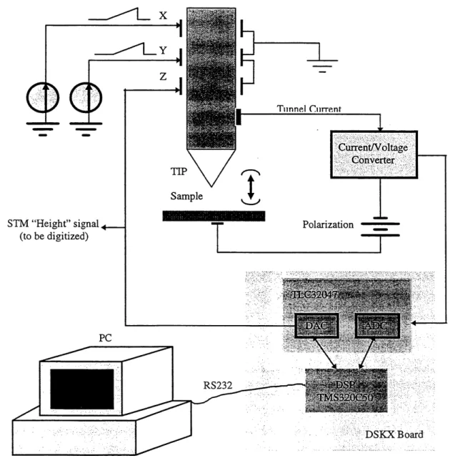
Our STM control system shown in figure 3.1 is based on the TMS320C50 DSP
processor. Compared to the analog control system described in figure 1.1, the new control board replaces the rectifier, the log amplifier, the set-point control, which is set through an appropriate user interface on the PC, and the Proportional Integral controller.
Since the purpose of this work was to evaluate the performance of the digital control loop, only this part is performed by the DSP board. The remainder of the STM functions, e.g. scanning signals generation, image acquisition, etc., are kept as they were with the existing analog control loop. Eventually, a complete digital control board, capable of scanning, digitizing the image, auto-calibration, etc. will be designed.
As shown in figure 3.1, the hardware of the STM digital control system mainly includes a PC, a control board DSKX, and RS232 interface between the PC and the DSKX. Through a dedicated application program written in the Lab View ™ development environment, the PC downloads the executable code onto the C50, launches execution, and communicates with the board.
The code running in real time on the C50 DSK board performs calibrations, implements the real time control loop, and tests dynamic characteristics (step test), etc.
The code running on the PC enables the user to interface with the control loop, to modify its configuration or its gains, to change the set-point, to launch a step test, to display the
data, etc. STM "Height" signal. (to be digitized)
t
l^uirent/^oltage^ NII^IG!cm^eTtCT^I%i Polarization DSKX BoardFigure 3.1 STM and the digital control loop
3.1 Hardware
3.1.1 Digital Control Board
The control loop is implemented and tested on a digital control board designed at the Universite de Sherbrooke.
This low cost DSP board, called DSKX, is built around, and adds functionality to, a Texas Instruments TMS320C50 DSK board. The total cost of the hardware, including the cost of Texas Instruments C50 DSK, is below 250.00 $. However, the performance of the system, in terms of analog signal integrity and quality, as well as digital processing power, is exceptional. The board has a small 4"x 4" footprint, and is connected to a PC via a RS232 serial link. Its small size, and the fact that it does not reside inside the PC, allow it to be conveniendy placed near the STM probe, thereby insuring low noise level for the acquisition electronics.
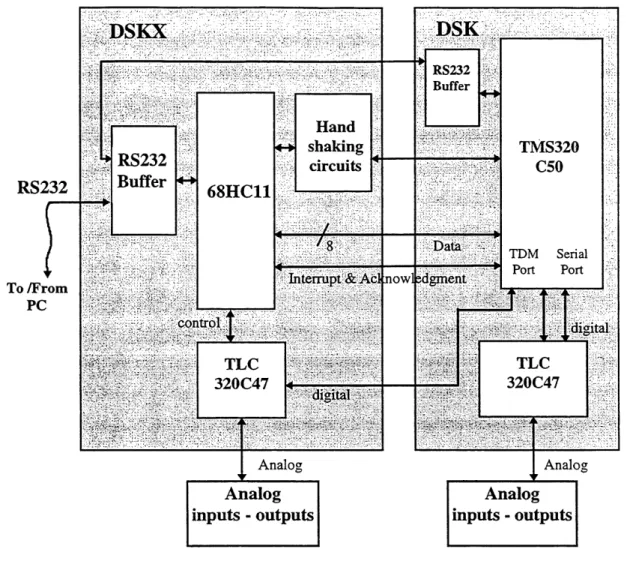
Figure 3.2 shows the block diagram of the DSKX board. The board mainly consists of a
MOTOROLA 68HC11 micro-controller, a TMS320C50 DSK board, and a high speed
A/D and D/A converter TLC320C47, which features switched-capacitor antialiasing input and output reconstruction filters.
The DSKX board contains all the necessary hardware to work stand alone for an autonomous application without the support from the host computer. However, in our application, we augment its functionality by connecting it to a PC or a Macintosh, which is the more usual way the board is used.
The 68HC11 and its surrounding circuits acts as the controller of the board. When the DSKX board is used as a stand alone processor or controller, the 68HC11 first downloads the application program to the DSK board, then launches the DSP execution. When the DSKX board is used as an attached processor or controller, the 68HC11 just acts as a communication controller between the PC and the DSK board.
RS232
To /FromPC
DSKX
68HC11
:ll^:?;S:/:iiH!]^£?i^;m^^rn^,
i[nteirai||^^j^^
S^i;^?^SIi^l<^tol;,:|isi^giiill
i|^^^i|||||||||j|||§|j|jji|iFI§;l||^^
DSK
iCData^|sdgmentjg|
—<1TMS320
C50
TDM Serial Port Port ^SS^SK vysl?i ftysB.|i||;ggj;||^||jjai|gital|
^^;?* ^ ^'::I •? ^<'^: ;•TLC
320C47
i^^§Slljl%S<8118^fcl^'s811^^^^ Analog AnalogAnalog
inputs - outputsAnalog
inputs - outputsFigure 3.2 Block diagram of the DSKX board architecture
The DSKX board has two modes of operation:
• Transparent mode
In transparent mode, the 68HC11 micro-controller is idle, permits the bi-direction communications between the DSK board and the PC directly. In general, this mode is used for the PC to download code to the C50 and launch an execution. Once the download has been done, the DSKX board will be set by the C50 to the second mode, C50-assistant mode, and all the functionalities of the 68HC11 are resumed.
C50-assistant mode
In the C50-assistant mode, the 68HC11 is mapped as a peripheral of the
TMS320C50, its I/O address is 0050h. The C50 can access the 68HC11
through reading and writing this I/O address. In this mode, all the functionalities of the board are administered by the 68HC11, and these
functionalities are controlled by the C50 by reading and writing 8 bits
commands and data to the address 0050h.
When the DSKX board is in C50-assistant mode, it works either in command mode or transmission mode. During the command mode, the 68HC11 expects one or more 8 bits commands coming from the C50. If data exchanges between the C50 and the DSKX board are required, the DSKX board changes to transmission mode after the 68HC11 finishes receiving commands from the C50, it expects the C50 to read or write a certain number of words from or to the memory 0050h, depending on what kind of command the C50 sends. There are 53 commands in all to administer the board functionalities, such as change the DSKX board mode, read or write registers, support the communication between the C50 and the PC, set the clock of the
TLC3204C47, etc.
When the DSKX board is in C50-assistant mode, it can also allow us to manage the bi-directional communication between the C50 and the PC. In each direction, there is a 128 bytes buffer. The FIFO of the 68HC11 functions as the "inter-station" between the PC and the C50, storing the data going to be read or written by the PC. The communication speed between the 68HC11 and
the PC is controlled by the C50 through writing the BAUD register of the
68HC11, the Baud rate could be 9600,19200,38400, 57600, etc.
The key features of this DSKX board are:
• TMS320C50, 40 Mips fixed point DSP with 10K words of RAM.
The TMS320 family processors are inexpensive alternatives to custom-fabricated VLSI and multi-chip bit-slice processors. Their valuable qualities, such as very flexible instruction set, inherent operational flexibility, high-speed performance, innovative, parallel architectural design and cost effectiveness, make this family the ideal choice for a wide range of processing applications.
The TMS320C50 DSP provides the following features:
1. 50ns single-cycle flxed-point instmction execution time
2. bit arithmetic logic unit (ALU), bit accumulator (ACC), and
32-bit accumulator buffer (ACCB)
3. 16-bit parallel logic unit (PLU)
4. 16x16-bit parallel multiplier with a 32-bit product capability
5. Single-cycle multiply/accumulate instructions
6. Full-duplex synchronous serial port for direct communication between the C50 and another serial device
7. Time-division multiple-access (TDM) serial port
With all these unique features and real-time performance, a C50 processor offers better, more adaptable approaches to traditional signal processing problems such as vocoding and filtering. Furthermore, the C50 supports complex applications that often require several operations to be performed simultaneously.
• High speed (up to 57600 Bauds ) bi-directional RS232 link with a PC.
This link has a 128 bytes buffer in each direction, and relieves the C50 from the task of managing communications with the PC. Therefore, the C50 can exchange data with the PC, while a control algorithm is running in real time on the C50.
• A TLC32047 high speed Analog to Digital and Digital to Analog Converter.
This economic, wide-band analog interface circuit (AIC) component is a complete interface system for advanced digital signal processors. It offers a powerful combination of options under DSP control: three operating modes combined with two word formats and synchronous or asynchronous operation. It provides a high level of flexibility in the conversion, sampling rates, filter bandwidths, input circuitry, receive and transmit gains, and multiplexed analog inputs under processor control.
The key features of the AIC are listed below: 1. 14-bit dynamic range ADC and DAC
2. 16-bit dynamic range input with programmable gain
3. Synchronous or asynchronous ADC and DAC sampling rates up to
25kHz
4. Programmable incremental ADC and DAC conversion timing adjustment
5. Switched capacitor anti-aliasing input filter and output reconstruction filter
6. Three fundamental modes of operation: Dual-word, word, and byte 7. Digital output in two's complement format
With all these advantages, it can be widely used in the fields of speech synthesis, process control, acoustical signal processing, spectral analysis, data
In STM control systems, the 14 bits digital interface can give us a 350(J.V resolution and noise for a 6V dynamic range. With the scan tube which is used, the 350pV resolution translated into a 0.035 A spatial resolution at the output, which is precise enough for the control loop.
3.1.2 STM Emulation
To facilitate the development of the algorithm, and the evaluation of the performance of the digital control loop, an emulator of the STM has been designed. This analog electronic circuit emulates the exponential behaviour of the tunnel junction, as well as the capacitive coupling between the piezo-electric drive signal and the input of the
current-to-voltage converter. Capacitive Coupling Input Exponential Amplifier Output ->
Figure 3.3 Block diagram of the electronic emulator
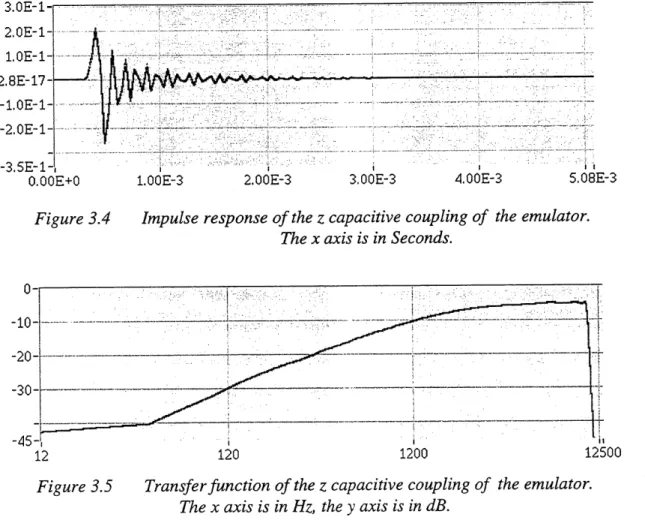
Figure 3.3 shows the block diagram of the STM emulator. The capacitive coupling is emulated using a simple analog differentiator, to which higher frequency poles are added to represent the cutoff frequency of the current-to-voltage converter, around 10 kHz.
Figures 3.4 and 3.5 show the impulse response and transfer function of the emulated capacitive coupling. In figure 3.5, the +20 dB/decade slope (around 1 kHz) is typical of a differentiator. Around 10 kHz, the higher frequency poles representing the cutoff of the current-to-voltage converter take effect. At 12 kHz, the sharp cutoff of the anti-aliasing filters used for the measurement is observed. With a -10 dB attenuation at 1200 Hz, this transfer function is representative of a 40 fF (femto-Farad) capacitive coupling, assuming an IV/nA current-to-voltage converter ratio, which is typical.
3. OE-1-] 2.0E-1-] l.OE-1-1 2.8E-17-] -l.OE-1-1 -2. OE-1-1 -3.5E-1-1.
O.OOE+0 l.OOE-3 2.00E-3 3.00E-3 400E-3 5.08E-3
Figure 3.4 Impulse response of the z capacitive coupling of the emulator. The x axis is in Seconds.
120
1200
12500
Figure 3.5 Transfer function of the z capacitive coupling of the emulator. The x axis is in Hz, the y axis is in dB.
The exponential function is implemented using a PN junction in the direct loop of an operational amplifier, which is in inverter configuration. Figure 3.6 shows the input/output relationship of the exponential part of the STM emulator. The gains of the
emulator have been adjusted so that the dynamic range is 3V both at the input and the output.
3.0-r-2.5-fc
2,0-1-1.5-E; 1.0-1- 0.5-1-0.0-II
':^^M^%li
SwSS SSSSi SSSiSigfi
®A i?u
31
<?%;11'1.-&1'.s
a
81
te; iyi3Sf' 0.0 0.2 0.4 0.6 0.8 1.0 1.2 1.4 1.6 1.8 2.0 2.2 2.4 2.6 2.8 3.0 Figure 3.6 Exponential input/output relationship of the emulator.The unit of x and y is Volt.
3.2 Software
As shown in figure 3.1, the DSP-based control loop leads itself to a division of tasks in which the DSK handles the STM control functions and the PC handles the user interface
and high level control. The code running on the DSK board is written in TMS320C50
assembly language and the code running on the PC is written in LabVEEW.
Lab VIEW is ideally suited for creating instrument drivers because it is a graphic language. We can model the panel of the instmment on a VI front panel and use the block diagram to send the necessary control commands to the instrument. It is very simple for the user to control the instrument by operating on the VI front panel. Furthermore, it has the outstanding advantage that we can use the instrument driver as a sub VI in conjunction with other sub Vis in a larger VI to control an entire system.
Figure 3.7 shows the structure of the program running on the PC. After the PC downloads the executable code to the DSK board, the code running on the PC first makes a simple
calibration to compensate the offset of the input channel of the ADC, then identifies the transfer function of the capacitive coupling with an adaptive LMS filter. Both the result of the calibration and identification will be applied to the real control loop on the C50. The control panel on the PC, as shown in figure 3.8, enables the user to interact with the control loop. It not only has a set of command buttons used to modify the configuration of
Reset
Modify PI
configuration and its gains
T
1
Download Executable Code to C50 and Launch the Execution
RS232 -^ DSK
Calibration
I
RS232^ DSK
Capacitive Coupling Identification
RS232
RS232 •^ DSK^ DSK
Change set-pointT
Open loop identificationT
Step perturbation testT
RS232 I RS232 I RS232 I RS232
DSK DSK DSK DSK
Figure 3.7 Architecture of the software running on the PC
the control loop, the gains of the PI controller, to change the set-point, to identify the open loop impulse response and store the coefflcients, to launch a step perturbation test, to display data, to stop the control loop, etc., but also enables the user to make a prediction of the open loop step response in simulation. The simulation result both in
polar and time plane are shown in the top-right and bottom graph in the control panel separately. This prediction can offer the user a rough idea of the optimized parameters, making the parameter adjustment process much easier and simpler.
setpoint -10000-ia -9000- -8000- -7000- -6000- -5000- -4000- -3000- -2000-
-1000-illlSiiiilHi"
?
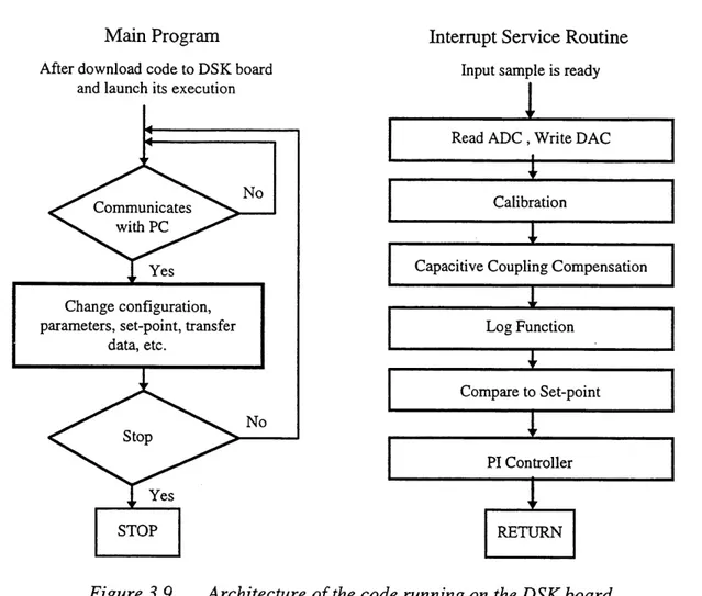
-?.o^%-4ap-fiai0|^ii sSSSSSS 2.0- 1.0- 0.0- -1.0--zo-'i -2.0 -1.0 05~i— :!25QOQ:',;1£y',,,.. Offset Frequence 0.0 2E+0-r 1E+0-5E-1-I OE+0-| -5E-1 -I -lE+O-'i -^ 6 1.0 2.0I I opeitobp.p3^ Y ' '.. t ^iimi ^^•^•"'^ WWSS^M 10 20 30 40 50 60 70 80 90 100 110 120 128 Figure 3.8 STM main control panel designed using LabVIEWFigure 3.9 shows the structure of the code running on the DSK board, including the main program and the interrupt service routine. As soon as the executable code is downloaded to the DSK board, it begins its execution by always checking the communication signal from the PC. A real time control interrupt service is triggered whenever a sample signal from the ADC is ready. In this subroutine, using the results coming from the calibration and capacitive coupling identification, the output signal of the ADC is adjusted to represent exactly the tunnel current, then a log function is applied to this signal to linearize the tunnel junction. By comparing the log result with the digital set-point, the input signal of the PI controller is obtained. Through the DAC, the output of the PI controller is applied to the piezo-actuator to adjust the Z position.
Main Program
After download code to DSK board and launch its execution
Change configuration,
parameters, set-point, transfer
data, etc.
No
Intermpt Service Routine
Input sample is ready
z
Read ADC , Write DAC
±
Calibration
I
Capacitive Coupling Compensation
I
Log FunctionI.
Compare to Set-point PI ControllerRETURN
Figure 3.9 Architecture of the code running on the DSK board
Note that since our DSKX board has a full duplex (bi-directional) on board serial ADC
and DAC, each time a sample signal is read from the ADC, at the same time, a control signal is written to the DAC. The control signal calculated in this interrupt routine will not be used until the next sample signal is ready.
Chapter 4. LOGARITHM CONTROL
The central part of a STM feedback control system is the PI corrector. Considering the exponential behaviour between the tunnel current and the tip-to-specimen distance, a logarithm function is inserted in the feedback loop. As a counterpart of the analog control loop shown in figure 1.1, figure 4.1 shows the block diagram of a digital tip-control loop.
^uH^tj^iytage:'! ^•!I^GoiiveEter^:<;;:':' STM "Height" signal <. (to be digitized) Controller Set-Point
Figure 4.1 Block diagram of the STM digital control loop
4.1 Linearization of the Tunnel Junction
Traditionally, two solutions are adopted to solve the problem of the non-linear relationship between the tip-to-specimen gap and the tunnel current:
• The first approach is to use the control loop in a small range around a fixed, and well known operating point. In this small range, the exponential behaviour of the gap-to-current relationship can be approximated by a linear function. Around this operating point, it is fairly straightforward to find fixed control parameters which yield a fast, stable closed loop system behaviour.
One problem of this approach is that the control parameters are only good around the considered operation point. If the actual tunnel current departs much from this operating range, the closed loop behaviour can become either over-damped, yielding a slow behaviour, or even worse, unstable. Typically, the system becomes more and more unstable as the gap is decreasing and the tunnel current is increasing, because the dynamic gain of the tunnel junction
becomes larger.
Another problem is that if the excursion of the system from its operation point is large, the response of the system becomes noticeably asymmetric.[71 In this case, the tracking of the surface is not as good when following an downward slope as when following an upward slope because of the exponential dependence of the tunnel current on the tip-to-specimen distance. This is especially true when the scanning speed is large.
• The second approach is to use a logarithmic amplifier to linearize the gap-to-current relationship, and obtain a perfectly linear, closed loop behaviour.
For this approach, there is a problem when the tunnel current is small. The analog logarithmic amplifiers are usually implemented with operational
amplifiers in an inverter configuration. It uses an exponential function (generally a PN junction) in its feedback loop. In such a configuration, the circuit has a static gain inversely proportional to the operating point, and a bandwidth inversely proportional to the static gain. With a large input, the gain of the log amplifier is small, and the bandwidth is large, therefore the time constant of the amplifier is short. However, with a small input, the gain is large, and the bandwidth is narrow, therefore the time response of the amplifier is long.
For example, for the model 755 from Analog Devices, the input can vary over 6 decades, from InA to 1mA. Correspondingly, the bandwidth varies from 80Hz (for a small current input) to 100kHz (for a large current input).
As the input becomes small, these systems will have the annoying tendency to become sluggish. For a STM, this happens when the tunnel current becomes small, i.e. when the microscope is operating with a large gap.
4.1.1 Digital Implementation of the Logarithm Function
For a digital control loop, the log function can be easily calculated for each incoming sample. It gives the following advantages:
• Since a log function is applied to the detected tunnel current, the system is linearized. Therefore, the closed loop behaviour of the control loop is independent of the operating point.
• Obviously, since the logarithm is computed numerically, its transient behaviour is independent of the value of the detected current.
A polynomial approximation is used to calculate the logarithm function. The advantage of this polynomial approximation over the more traditional lookup table131 is its precision. For an input with dynamic range of 16 bits, the log function has an output with dynamic range of 13 bits, precise to 1 LSB (least significant bit). To implement the same function with the same precision by a lookup table would have taken a 64Kwords-long table. The disadvantage of this solution is that it is a little more computationally expensive than a lookup table.
In the polynomial approximation, let 0<X<1 represents the 16 bit number we are going to calculate the log of. To guarantee the high precision with a flxed-point DSP processor, we need first to normalize the input X. Normalizing this fixed-point number means to represent it by two parts, a mantissa and an exponent. This is done by finding the magnitude of the sign-extended number.
Let
Shift = number of left shift(s) needed to normalize X (4-1)
Y=2shiftX (4-2) The normalized result of X is to make Y in the range of [0.5, I], and the value of Shift is in the range of [0, 16].
Then
log,oX=log,oY-log,o2shl(t
=logio(2Y)-K(Shift+l)
= a, (Y-0.5)+a2 (Y-0.5)2 +a^ (Y-0.5)3 +84 (Y-0.5)4 (4-3)
+as(Y-0.5)5-K(Shift+l)
Where
a^ = 0.8678284, a^=-0.8511354, 83 =0.9925536, a^=-0.9245608,
as = 0.4360352, K = 0.301029995
Let
A = ((((a^ (Y-0.5)+ a, )(Y-0.5)+ a, )(Y-0.5)+ a^ )(Y-0.5)+ a, )(Y-0.5) (4-4)
Where A is in the range of [0, 0.3010], B is in the range of [0.3010, 5.117].
Then
log 10 X = A-B is in the range of [-5.117, 0] Therefore
log^X should be in the dynamic range of 15-bits.
(4-6)
Appendix B is the code used to calculate the polynomial approximation of the log function. It costs 22 additions/subtractions, 6 divisions and 12 multiplications. On a DSP
like TMS320C50, this can be easily done between 2 incoming samples at 25 kHz
sampling rate.
-6000-
-8000--10000-L. - i_- "_J::"; ;':T;! :':r:l:u''ifJ_^''l'_l_ J__ J__ J_. __" 0.000 0.100 0.200 0.300 0.400 0.500 0.600 0.700 0.800 0.900 0.999
Figure 4.2 Digital logarithm function result. The y axis is in numerical
representation
0.0-
-0.2-0.000 0.100 0.200 0.300 0.400 0.500 0.600 0.700 0.800 0.900 0.999
Figure 4.3 Computation error of the digital logarithm function The y axis
is in numerical representation.
Figure 4.2 shows the result of the digital log function in the range of (0, 1). Notice that the y axis is in numerical representation with the dynamic range of 15 bits. The actual log
result can be obtained by dividing the value of y axis by 2048. The computation error is shown in figure 4.3. We can see that the approximation of the log function is in high precision, the computation error is within 1 bit.
For a particular implementation, if the necessary computation power is not available, either because the processor chosen does not have as much computational power as TMS320C50, or because the processor is also busy on doing other real-time tasks, a lookup table with less precision than what we used may probably give the same overall performance. Actually, the log function is only needed to linearize the exponential behaviour of the junction, so as to keep the closed loop transient behaviour of the STM relatively insensitive to the operating point. Since the system is a closed loop, and it incorporates an integrator in the feedback loop, the steady state error will go to zero eventually regardless of the precision of the logarithm.
-1000
2.0 2.2 2.4 2.6 2.8 3.0 -10000-1,
0.0 0.2 0.4 0.6 0.8 1.0 1.2 1.4 1.6 1.
Figure 4.4 Exponential function of the STM emulator, linearized by a computed logarithm function. The x scale is in Volts, the y scale represents the output of the log
function, and is in arbitrary fixed point representation
Figure 4.4 shows the static input/output relationship of the exponential emulator followed by the log function. This figure was obtained by following procedure:
• Sending a ramp on the DAC, to the input of the exponential function of the
• Digitizing the output of the exponential function using the ADC • Applying the numerical logarithm to the sampled values.
Notice that the quantization of the signal is very apparent and coarse in the lower left comer of the graph, where the input signal of the ADC (the output of the exponential function) is small. This is a normal behaviour, due to the high dynamic gain of the log function near a zero input. Notice also that the combined transfer characteristic, including the analog exponential function followed by the numerical logarithm, is very linear, which is very important to the STM control loop.
4.1.2 Problems Due to the Input Offset Bias
When the control loop is operated with a small set-point, which means that a large gap would lead to a small tunnel current, the offset bias of the input channel should be kept at a very small value. When the tunnel current is small, the log function has a high dynamic gain. Therefore, in this case, a small static offset error on the input signal can lead to a large difference on the value of the log, making the combined behaviour of the exponential and log function very non-linear around this operating point.
For traditional instmments, to keep the offset of the analog input chain to a small value, requires the use of expensive precision operational amplifiers, or the use of noisy chopper stabilized ones, and even then, the offset (and its temperature drift) is still not negligible. On the other hand, for a completely digital control loop, a very simple offset calibration procedure can be implemented by software as follows:
• Just before scanning a new image, retract the tip as far as possible (far enough so that the tunnel junction is broken).
• At this point measure the voltage at the input channel. Since the tunnel current is zero, this represents the offset of the input channel.
• Keep this value in memory, and from that point on, subtract it from any input value acquired during the operation of the control loop.
• Lower the tip, to create the tunnel junction again, and re-engage the control
loop.
• Acquire the image fast enough so that the offset does not have time to drift noticeably.
Based on this calibration procedure, the input offset bias problem can be solved very well and without time or temperature drift.
4.1.3 Problems Due to the Rectifier
On most STM implementations, the need to operate with a choice of positive or negative polarization of the specimen leads to the use of a precision rectifier. This rectifier, which is usually installed in the path of the input channel just before the log function, keeps the sign of the detected current positive, no matter what the sign of the specimen polarization is. The input of the log function is therefore always positive. It is directly proportional to the absolute value of the detected current.
In our digital control loop, we first implemented this precise rectifier by software. A simple absolute value operator is applied directly to the output of the ADC. However, the problem of this solution is that any high frequency noise present on this input is rectified by the absolute value operator, and it is seen at the input of the log function as a static bias (or offset). This bias limits the operability of the control loop at small tunnel currents, since it makes the behaviour of the control loop non linear around this operating point (problem discussed earlier).
Instead of implementing an absolute value at the input of the log function, we opted for a fixed sign, adjusted in conjunction to the sign of the polarization. The automation of the
adjustment of this sign only requires that the specimen polarization voltage be under the control of DSP. Under this solution, high frequency noise on the input channel will not act as a bias on the detected input voltage. It will still, however, degrade the quality of the acquisition, but not that much, since the integrator part of the controller will tend to average it out. We obtained a much better result with this solution than the fomier one.
4.2 PI Corrector
After the Unearization of the exponential dependence between the tunnel current and the tip-to-specimen distance, a simple PI corrector is employed to control the voltage applied to the Z actuator.
In control theory, a typical PID feedback controller implements the equation:
dY.
V.« = KpV,.(t)+K,J V,.(t)dt+Kt>^—^ (4-7)
Where Kp, K| and Kp are the gains of P, I and D correctors separately. In our system, V is the logarithmic error signal after compared to the set-point, and Vo^ is the control voltage after DAC and further amplification, which adjusts the tip-to-specimen distance. This expression is slightly more general than the integral filter usually used in STM control systems. "Hardware" PED process controllers can, of course, be constmcted, but it has much less flexibility than by DSP. In our digital feedback control system, the coefflcients Kp, K| and Kp can be adjusted at any time during operation, providing real time control over the feedback loop.
Considering the effect of P, I and D separately, proportional feedback responds quickly to small features but cannot maintain a zero DC error. Integral feedback maintains a zero DC error but cannot respond to small features without oscillating. Derivative feedback
reduces overshoot and oscillation, but at the same time, it will amplify high frequency noise in the STM current measurements, that makes the use of the derivative feedback impractical. In our system, another reason to remove the D corrector is to reduce the computation time for the interrupt service routine on the C50, so that we can run the real time control loop with the highest possible frequency.
To implement the PI controller in the digital domain, suppose the input signal is sampled at a frequency f g , giving a sample interval T = 1/f g . A discrete representation of the controller can be written as:
Y(n)=P(n)+I(n) (4-8)
P(n) = KpX(n) (4-9)
I(n)=K/T^X(k) (4-10)
X(n)=C(n)-S (4-11)
Where n represents the time index nT, X(n), Y(n) are the discrete input and output of the PI controller, P(n), I(n) are the outputs of P , I correctors separately. C(n) is the logarithmic value of ADC reading (after further adjustment), S is the set-point.
For the I controller, Eq. (4-10) can be rewritten explicitly in the form of an Infinite
Impulse Response (HR) filter as:
I(n) = K/TX(n) +I(n - 1) (4-12)
In our digital controller, Kp, K| and S are all in the format of 16 bits fixed-point number representation. The adjustable range of Kp and K, is [6.25E-4, 6.25], and S can be adjusted in the range of (-10000, 0) (arbitrary fixed point representation), corresponding to the output range of the log function, which is (-9248, 0). For a DSP
capability, the digital PI controller can be implemented simply and precisely. It only requires a couple of buffers to store the last output of the I controller I(n-l), which is 32 bits fixed point number. For an input with 16 bits dynamic range, all of the intermediate PI controller computation result is in 32 bits, so the output of the controller has a relatively high precision, which makes the control behaviour very smoothly.
During scanning process, Kp, K| and S can be set at any time by the user. The feedback gain controls the response rate of the feedback: when it is too low, the feedback responds slowly and features wash out; when it is too high, the feedback overshoots and oscillates.
To optimize Kp and K, , we use a simple and precise procedure to predict the control loop behaviour by deriving the open loop impulse response from the closed loop step response, which will be described in detail later. Once the feedback coefficients are optimized, we can fix them and apply them to the real time control loop.
Chapter 5. CAPACITIVE COUPLING COMPENSATION
During scanning and acquisition of the image, it is normally assumed that the current detected in the microscope stylus is only the tunnel current. However, in practice, the detected current contains not only the tunnel current, but also the current which comes from the capacitive couplings between the electrodes of the piezo-actuators and the input of the current-to-voltage converter. The capacitively coupled current is often considered as noise to the input channel. However, it has an impact on both the quality of the image and the stability of the control loop.
Figure 5.1 shows the block diagram of the real system, in which the capacitive couplings between the electrodes and the input of the current-to-voltage converter are illustrated.
Even if great attention is paid to the shielding of the stylus from the electrodes and the geometric arrangement of the piezo-actuators and the stylus, it is still very difficult to reduce this stray current to a relatively negligible range. To have an idea about the range of the phenomenon, let's consider a stray capacitance of no more than 0.1 pF. With a control voltage of IV peak on the electrodes of the piezo motors, at a frequency of 1 kHz (which correspond to normal practical conditions), this capacitance will inject a current of 0.6 nA peak into the stylus. This stray current is well within the normal detection range of
the tunnel current.
Inspired by the active noise cancellation techniques, we use a similar solution to solve this problem in our digital control system. If the signals applied to the different electrodes of the piezo motors are generated by the control system, they are perfectly known and controlled. The transfer functions and the impulse responses of the 3 capacitive couplings between the X, Y and Z signals and the input of the current-to-voltage converter can be identified before the control is engaged. From these identified models and the knowledge of the actuation signals, the stray currents from the capacitive couplings can be
determined perfectly by the controller in the digital domain, and can be subtracted from
the measured tunnel current.
Digital Domain STM "Height" signal <• (to be digitized) Rectifier
)_
<"ADC.W
dfc ,^,-'':L6g^l::^''-1^^ Controller Set-PointFigure 5.1 Block diagram of the capacitive coupling between the electrodes of the
piezo-actuators and the input of the current-to-voltage converter.
In this chapter, we will first describe the problem and symptoms coming from the capacitive coupling , then introduce the normalized LMS (least mean square) algorithm to identify its transfer function, finally the compensation procedure and results are discussed.
5.1 Problem and Symptoms
It is well known that the transfer function of the capacitive coupling is mainly a differentiator, with its effect being more obvious at higher frequencies. In STM control system, the capacitive coupling comes from two sources:
• The coupling from the scanning voltages (X and Y signals).
The scanning voltages are essentially ramps, with a fast ramp on X, and a slow ramp on Y. Since the X ramp is much faster than the Y ramp, the corresponding stray current in the X direction is much more important than in the Y direction. In this case, since the disturbance voltage is a ramp, the stray current, which sign depends on the scanning direction, is close to a constant bias (except at the edges of the image). In other words, the scanned profile of the specimen appears to be raised when scanned from left to right and lowered when scanned from right to left. Since the scanning voltages are independent of the scanned profile, so is the coupled current. This component of the stray current is actually equivalent to an added noise on the tunnel current and has an impact only on the quality of the image.
• The coupling from the Z voltage (Z control loop).
The Z voltage is the output of the PI controller. Therefore, this capacitive coupling has an impact on the closed loop behaviour of the system. In fact,
this capacitive coupling comes in parallel to the tunnel junction. Since the coupling is a linear transfer function, and its output is added to the tunnel current which is fed to the log function, the component of the input of the PI controller, which comes from the capacitive coupling, is non linearly related to the voltage at the Z actuator.
The net effect of the capacitive coupling is to make the open loop transfer function of the controlled system (from the voltage at the Z actuator to the output of the log function) non linear. This can lead to variable behaviours at different operating points, with a potendal for instability. This is exactly what the log function is supposed to avoid in the first place.
Also, when the control algorithm reacts to push the tip towards the surface, possibly in response to a widening of the gap, the resulting stray current is mixed to the tunnel current. Depending on the sign of the polarization of the specimen, this stray current can be added or subtracted from the tunnel current. In case it is subtracted, this can confuse the control algorithm into "thinking" that it is farther away from the surface than it really is. In this case, the control algorithm will overshoot, and possibly hit the surface.
The component of the capacitive coupling in Z direction is obviously problematic. Not only does it degrades the quality of the image, as does the capacitive coupling from the scanning voltages (X and Y signals), but also it can result in instabilities, or dangerous overshoots in the behaviour of the closed loop system.
Since the purpose of this work was only to evaluate the performance of a digital control loop, only the Z capacitive coupling was identified and compensated. In a real instrument, all three X, Y and Z channels should be properly compensated, which multiplies the computational complexity by three.
To be able to compensate properly the capacitive couplings on the X and Y axes in the digital domain, the scanning voltages should be generated by the same control system (DSP) which processes the tunnel current input, and by DACs operated at the same sampling frequency and synchronously to the ADC of the input channel. Only in this case will the transfer functions of the capacitive couplings be identifiable and be usable in the digital domain.
5.2 Capacitive Coupling Identification with the LMS Algorithm
Since the transfer function of the capacitive coupling is mainly a different! ator, we can model it with a FIR filter. Figure 5.2 shows its adaptive FIR modeling. The optimization algorithm we use in our system is a normalized LMS algorithm,1 1[] which is an important member of the family of stochastic gradient algorithms. The practical importance of the LMS algorithm is basically due to its two unique attributes:
• Simplicity of implementation. Its light computational load make it easy to be implemented in real time on the DSP.
• Model-independent and therefore robust performance.
The process of the LMS algorithm consists of two basic parts:
• A filtering process, which involves computing the output of a transversal filter produced by a set of tap inputs, and generating an estimation error by comparing this output to a desired response.
• An adaptive process, which involves the automatic adjustment of the tap weights of the filter in accordance with the estimation error.
x(n) Input System to be identified ^systen/model +
y(n)
Q
e(n)^~
f"y(")
LMS
ive weight-control :„ : ;? ;:: mechanismFigure 5.2 System identification based on FIR model and LMS algorithm
As illustrated in figure 5.2, we supply the system to be identified with a input sequence x(n) and observe its output sequence y(n), which is the desired response that provides a reference for the optimum filtering action. At time n, the estimate of the desired response
y( n), which is modeled by an HR filter, can be computed as :
L-l
y(n)=I>(k)x(n-k) n=l,2,..,N (5-1)
k=0
where N » L - 1. h(0), h(l),...h(L-l) are the corresponding L coefficients of the FIR to be adjusted.
Equation (5-1) can be rewritten as the inner product of the weight vector H and the input vector X(n).
y(n)=X(n)TH
(5-2)
where
HT =[h(0),h(l),H(2),...h(L-l)] (5-3)
X(n)T=[x(n),x(n-l),x(n-2),...x(n-L+l)] (5-4)
By comparing the estimate with the desired response, we produce an estimation error denoted by e(n). We may thus write
e(n)=y(n)-y(n)
i.e.
(5-5)
(5-6)
e(n)=y(n)-X(n)TH
Let the mean square value of the error signal be denoted by
J=E[e2(n)] (5-7)
This mean square value is a real and positive scalar quantity, representing the average power of the error signal e(n). It is a function of the coefficient vector H. The gradient vector VJ can be attained as
,. 3E[e2(n)]
3H
3E[e2(n)] 3E[e2(n)] 3E[e2(n)]
3h(0) 3h(l) 3h(L-l)
Equation (5-8) can be simplified as
3e(n)~
V;J = 2E
=2e(n)
e(n)
3H
3e(n)
' 3h(0)
From equation (5-6), the gradient
e(n)
3e(n)
3H
3e(n)
3h(l)
e(n)
3h(L-l)
3e(n)
can be simply expressed as
3e(n)
3H
=-X(n) thenV;J=-2E[e(n)X(n)]
(5-8)
(5-9)
(5-10)
(5-11)
According to the method of steepest descent, the updated value of the coefficient vector is computed by using the simple recursive relation
H(i +1) = H(i) - HVj(i) = H(i) + 2jiE[e(n)X(n)] (5-12)
where i indicates the optimization iteration, in general, we make an iteration of optimization for each new sample signal, so n and i will be equal. The parameter ji controls the behaviour (speed and stability) of the optimization. Briefly, if p. is too small,