HAL Id: hal-02085776
https://hal.archives-ouvertes.fr/hal-02085776
Submitted on 12 Apr 2019
HAL is a multi-disciplinary open access
archive for the deposit and dissemination of
sci-entific research documents, whether they are
pub-lished or not. The documents may come from
teaching and research institutions in France or
abroad, or from public or private research centers.
L’archive ouverte pluridisciplinaire HAL, est
destinée au dépôt et à la diffusion de documents
scientifiques de niveau recherche, publiés ou non,
émanant des établissements d’enseignement et de
recherche français ou étrangers, des laboratoires
publics ou privés.
Parameterization Models for Traceable Characterization
of Planar CPW SOL Calibration Standards
F. Mubarak, V. Mascolo, G. Rietveld, M. Spirito, K. Daffe, K. Haddadi
To cite this version:
F. Mubarak, V. Mascolo, G. Rietveld, M. Spirito, K. Daffe, et al..
Parameterization
Mod-els for Traceable Characterization of Planar CPW SOL Calibration Standards.
2018
Confer-ence on Precision Electromagnetic Measurements (CPEM 2018), Jul 2018, Paris, France. pp.1-2,
�10.1109/CPEM.2018.8500810�. �hal-02085776�
Parameterization Models for Traceable Characterization of Planar CPW
SOL Calibration Standards
F. Mubarak
1, V. Mascolo
1, G. Rietveld
1, M. Spirito
2, K. Daffe
3and K. Haddadi
3 1VSL, Van Swinden Laboratorium, Delft, The Netherlands, E-mail:
[email protected]
2Delft University of Technology, Electronic Research Laboratory (ERL), Delft, The Netherlands
3Université Lille 1, Institut d'Electronique, de Microelectronique et de Nanotechnologie (IEMN), France
Abstract — Methods for traceable characterization and uncer-tainty evaluation of planar 1-port CPW short-open-load (SOL) devices are developed. The agreement of modelling and verifica-tion measurement results greatly supports the applicaverifica-tion of the proposed parameterization models and used FEM-based EM modelling of CPW structures for traceable characterization of planar CPW-based SOL devices in the frequency range between a few kHz up to 50 GHz.
Index Terms — nanostructures, co-planar waveguide, on-wafer calibration, EM simulation, VNA, measurement uncertainty, precision measurements, traceability.
I. INTRODUCTION
For the high-frequency characterization of nanostructures and nanoscale devices, accurate vector determination of measurement system errors of probing stations is crucial to achieve reliable results. Unlike for coaxial and waveguide interfaces, traceability is not well-established for S-parameter measurements in a planar environment. Here, accuracy is hampered by the wide range of substrate materials, with non-identical electrical and mechanical parameters, and different RF probe topologies and pitches.
In [1], the probe-to-substrate interaction is identified as the dominant uncertainty source in transfer of traceability between different substrate materials. Furthermore, accurate definition of the measurement reference plane position is critical for probe-independent characterization of device S-parameters [2]. In [3], the use of method-of-moments based EM modelling of short-open-load (SOL) standard definitions resulted in a signifi-cant enhancement of calibration accuracy in comparison to the classical lumped model. Recently, [4] reported progress towards establishing traceability for a planar environment together with detailed uncertainty budgets.
In this paper, we report our progress towards traceable characterization of nanoscale devices, via parametrization of planar SOL devices that can be used to calibrate RF measure-ment heads of probing stations. First, a model parametrization is carried out to identify the critical parameters for subsequent FEM-based EM modelling of the SOL structures. Then, the uncertainties of the various device parameters are propagated through EM simulations to obtain the complex reflection coefficient Г with corresponding uncertainty u. A dedicated measurement experiment is outlined for validation of the proposed modelling approach.
II.PROPOSED CPWMODELS
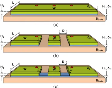
Measurement models suitable for characterization of planar SOL calibration standards have been developed. Each model identifies critical parameters necessary for traceable characteri-zation of the input reflection-coefficient (Г) parameter. Fig. 1 gives a cross-sectional overview of CPW-based SOL cali-bration standards together with the dimensional parameters necessary for characterization of Г.
(a)
(b)
(c)
Fig. 1 Cross section of a CPW-based (a) short device, (b) open device and (c) nominal 50 Ω load device.
The SOL structures consist of a thin layer of resistive material located below metallic contacting pads to form the desirable impedance for the load device. The reference plane of each device is fixed on top of Co-Planar Waveguide (CPW) contact pads, depicted with red dots in Fig. 1. These are the positions where the probe tips are expected to contact the CPW device. Hence, the pitch size of the probe is a crucial parameter for characterization of a CPW device.
III. Traceable Parameterization Techniques
In order to determine the critical parameters of the planar SOL calibration standards, an optical microscope is used for measurement of the majority of the critical dimensional para-meters of the CPW structures. For the height parapara-meters Ht and
Hg, a white-light interferometer is used. The sheet resistance is
measured using a standard 4-point measurement technique. In
W L Hg δGaAs Ht , δTi δg Hg W L D Wi δGaAs Ht , δTi δg Hg W L D Ht , δTi Wi Lt δGaAs δg
Table I, the resulting device parameters with corresponding uncertainties are shown.
TABLE I
PARAMETER MEASUREMENT VALUES FOR CPW SOL DEVICES
Parameter Short Meas. [nom] Open Meas. [nom] Load Meas. [nom] Uncertainty (k=2) Hg (nm) [500] [500] [500] na L (μm) 92 [92.5] 91 [92.5] 91 [92.5] 2 W (μm) 825 [830] 301 [300] 300 [300] 2 Wi (μm) na 100 [100] 101 [100] 2 D (μm) na 61 [60] 61 [60] 2 Ht (nm) 23 [23] 23 [23] 23 [23] 1 Lt (μm) 92 [90] 91 [92.5] 91 [92.5] 2 ꝽRes. (Ω) na na ~50 [49.1] 5%
The parameterized model is subsequently designed in CST Microwave Studio (CST) software for FEM-based EM simulation of the planar SOL structures. The model parameter uncertainties are propagated through EM simulations to acquire consistent device Г-values with corresponding uncertainty u. The structure excitation is based on lumped ports with distances corresponding to actual probe-pitch sizes, with an infinitely-expanded dielectric substrate. A point voltage source with 50 source impedance is applied to a perfect electrical conductor bridge to achieve a transition identic to actual probe based excitations. The entire structure is simulated using a frequency domain solver that supports a tetrahedral mesh, in combination with localized refinement to increase the mesh density in critical parts of the SOL devices. The maximum step width is chosen to properly mesh the shortest model edges (23 nm for the resistive layer) and to account for parameter variation. A second-order solver is selected with an accuracy of 1e-9. Starting from initial mesh settings, the mesh is refined until the convergence criteria for each frequency point are satisfied (∆S = 0.01). The material properties, such as the Au and GaAs conductivity, are derived from the CST library.
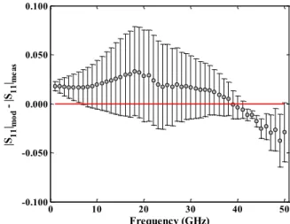
IV.MEASUREMENT EXPERIMENTS &DISCUSSION
First, ГS,O,L-values with corresponding uncertainty uS,O,L are
derived from EM simulations of parameterized models for a set of SOL devices. These are then used for 2-port unknown-thru calibration of a VNA and subsequently S11(meas) of an
offset-short device in the 1 – 50 GHz frequency range is measured. Afterwards, the measurement results S11(meas) are compared with
reference values S11(mod) derived using the proposed EM
simulations based characterization technique. The difference of the measurement results with respect to the model results is depicted in Fig. 2. The uncertainty bars uOS result from linear
propagation of the standard uncertainties uS,O,L (derived with
the proposed method) through the unknown-thru calibration. For a considerable part of the frequency range, the differences shown in Fig.2 agree within the uncertainty contributions resulting from the SOL calibration artifacts. Nonconformity for some results might be caused by incorrect
exclusion of certain uncertainty contributions, such as probe repeatability and frequency dependent conductivity of the used materials. In addition, for the highest frequencies, the omission of the coupling between the two on-wafer probes likely plays a role as well. Present research is being performed to improve our uncertainty budget accordingly.
V. CONCLUSION
We have successfully developed parameterization models and an EM-simulation based characterization approach for CPW-based SOL devices. The first results of a comparison between these models and measurement experiments show considerable agreement and form the basis for our future work.
ACKNOWLEDGEMENT
This work was funded through the European Metrology Research Programme (EMPIR) Project PlanarCal ‘Metrology for New Electrical Measurement Quantities in High-frequency Circuits’ and the Dutch Ministry of Economic Affairs. The EMPIR is jointly funded by the EMPIR participating countries within EURAMET and the European Union.
REFERENCES
[1] L. Galatro and M. Spirito, “Analysis of residual errors due to calibration transfer in on-wafer measurements at mm-wave frequencies”, IEEE Bipolar/BiCMOS Circuits and Technology
Meeting – BCTM, Boston, MA, 2015.
[2] L. Galatro, F. Mubarak and M. Spirito, “On the definition of
reference planes in probe-level calibrations”, 87th ARFTG
Microwave Measurement Conference (ARFTG), CA, 2016.
[3] M. Spirito, L. Galatro, G. Lorito, T. Zoumpoulidis, F. Mubarak, “Improved RSOL Planar Calibration via EM Modelling and
Reduced Spread Resistive Layers”, 86th ARFTG Microwave
Measurement Conference, Atlanta, GA, 2015.
[4] U. Arz, S. Zinal, T. Probst, G. Hechtfischer, F. J. Schmückle and W. Heinrich, "Establishing traceability for on-wafer S-parameter measurements of membrane technology devices up to 110 GHz," 2017 90th ARFTG Microwave Measurement
Symposium (ARFTG), Boulder, CO, USA, 2017, pp. 1-4.
Fig. 2 Difference between Г measurement values and model results for an CPW offset-short device fabricated for verification along previously characterized SOL devices (gray dots).
0 10 20 30 40 50 -0.100 -0.050 0.000 0.050 0.100 Frequency (GHz) |S11 |mod |S11 |mea s