O
pen
A
rchive
T
OULOUSE
A
rchive
O
uverte (
OATAO
)
OATAO is an open access repository that collects the work of Toulouse researchers and
makes it freely available over the web where possible.
This is an author-deposited version published in :
http://oatao.univ-toulouse.fr/
Eprints ID : 13985
To link to this article : DOI:10.1016/j.snb.2014.07.088
URL :
http://dx.doi.org/10.1016/j.snb.2014.07.088
To cite this version : Chapelle, Audrey and El Younsi, Imane and
Vitale, Stefania and Thimont, Yohan and Nelis, Thomas and
Presmanes, Lionel and Barnabé, Antoine and Tailhades, Philippe
Improved semiconducting CuO/CuFe2O4 nanostructured thin films
for CO2 gas sensing. (2014) Sensors and Actuators B: Chemical, vol.
204. pp. 407-413. ISSN 0925-4005
Any correspondance concerning this service should be sent to the repository
administrator:
[email protected]
Improved semiconducting CuO/CuFe
2
O
4
nanostructured thin films for
CO
2
gas sensing
A. Chapelle
a, I. El Younsi
a, S. Vitale
b,c, Y. Thimont
a, Th. Nelis
b, L. Presmanes
a,∗,
A. Barnabé
a, Ph. Tailhades
aaInstitut Carnot CIRIMAT–UMR CNRS 5085, Université Paul Sabatier Toulouse III, 118 route de Narbonne, 31062 Toulouse Cedex 9, France bBern University of Applied Sciences, Engineering and Information Technology, rue de la source 21, 2501 Bienne, Switzerland
cDipartimento di Scienze Chimiche, Universita’ di Catania, Viale A. Doria 6, 95125 Catania, Italy
a b s t r a c t
Promising results on the behavior of CuO/CuFe2O4sputtered thin films as a sensing material under carbon
dioxide atmospheres are presented in this article. More specifically, we report the effects of preparation parameters and microstructure of the sensing layer on the response to CO2. FEG-SEM images and XPS
measurements revealed the two-stacked layers rearrangement of samples after air annealing as a key parameter in gas sensing test. The influence of the sensing layer thickness and the influence of Ag as an additive in the film on the response are also reported. The best response was obtained at the optimal operating temperature of 250◦C with a thin film deposited under low argon pressure and low
target-to-substrate distance, reaching 40% towards 5000 ppm of CO2.
1. Introduction
Semiconductor nanocomposites with p–n junction were reported in the literature as the most performing materials for gas sensing regarding operating temperature and response. Ishi-hara et al.[1]introduced the CO2 gas sensing using a composite
oxide/BaTiO3junction. Several studies were performed on the
com-parison of different oxides combined with BaTiO3 such as PbO,
MgO, CaO, NiO or CuO[1]. As a result, CuO/BaTiO3 exhibited the
highest response to CO2with a relatively low operating
temper-ature in comparison with other oxides. Other groups replaced the perovskite phase by either another perovskite phase[2] or other oxides having rutile structure[3,4]. From then on, several research groups worked on this composite[5–8]by changing the way of elaborating this material. Indeed, many studies have been carried out on thin[5,9,10]and thick films[1,6,8,11]. Thin films show higher repeatability in fabrication process, better control on fabrication parameters and better conditions in mass production, which allows lower costs than thick film techniques. In this work,
∗ Corresponding author.Tel.: +33 5 61 55 81 03; fax: +33 5 61 55 61 63 E-mail address:[email protected](L. Presmanes).
radio-frequency (RF) sputtered CuO/CuFe2O4semiconductor thin
films are used as sensitive material. It has been already demon-strated[12]that the CuO/CuFe2O4composite was sensitive to CO2.
In the present work, some of the key aspects concerning the electric response under CO2of CuO/CuFe2O4thin-films are
corre-lated with the microstructure characterization thanks to scanning and transmission electron microscopy and X-ray photoelectron spectroscopy analyses. The effects of preparation parameters, microstructure, as well as the influence of silver doping on the sensitivity of the CO2sensor are also described.
2. Experimental
2.1. Preparation of the gas sensitive elements
Thin films were deposited by RF-sputtering technique using a CuFeO2 ceramic target according to the preparation described
by Chapelle et al. [13]. Thickness calibrations were performed with a Dektak 3030ST profilometer. Process parameters for the as-deposited samples are given in Table 1. In order to obtain the CuO/CuFe2O4 nanocomposite, the as-deposited films were
annealed at 450◦C in air for 12 h. After heat treatment, gold
Table 1
Summary of deposition parameters.
Referencing of deposition conditions P0.5d5 P2d8
Target material CuFeO2
Substrates Fused silica glass, silicon, quartz
Power (W/cm2) 3.5
Argon pressure P (Pa) 0.5 2.0
Target to substrate distance d (cm) 5 8
P × d (Pa cm) 2.5 16
Deposition rates (nm/min) 6.77 3.75
(DC)-sputtering. Finally, our simplified test device consisted of a substrate, the oxide sensitive layer and two gold electrodes.
2.2. Microstructural characterizations
The microstructure of thin films were examined with a Jeol 2100 field emission gun Transmission Electron Microscope (TEM) and a Jeol JSM 6400 field emission gun Scanning Electron Micro-scope (SEM). A Thermo Scientific K-Alpha apparatus was used for X-ray photoelectron spectroscopy (XPS) measurements, using a monochromatic Cu Ka radiation with a 400 mm spot size. Peaks were scanned at 50 eV pass energy. The spectrometer was equipped with ions gun to realize depth profile by etching technique. Flood gun was used to minimize charging effects. The binding energies (BE) were referenced to the 1s carbon peak (atmospheric con-tamination) at 284.6 eV. The structure of thin films was examined by Glow-Discharge Optical Emission Spectrometry (GD-OES) mea-surements. GD-OES allows fast compositional depth-profiling from the nanometer range up to several hundreds of micron in depths. The depth resolution of this technique is of a few nanometers for thin layers, but increases for thicker layers to reach a few percent of the total sputtered depth. The major advantages of the technique are its speed and ease of use. The optical emission measurements were all conducted on the instrument referred to elsewhere[14], a Jobin Yvon JY 5000 RF instrument equipped with a Hi LightTM
133-Dressler GmbH 13.56 MHz RF generator capable of supplying constant real power, constant applied RF-voltage, or constant DC-bias voltage, and also capable of being operated with continuous or pulsed RF power.
2.3. CO2sensing measurements
The impedance of the sensing layer was measured by a Fluke PM6306 RCL-meter. The experiments were carried out from room temperature to 500◦C, using a tube-type furnace with a
pro-grammable temperature controller. The total gas flow was fixed at 100 cm3/min. Two gas bottles were used, one with synthetic dry air
Fig. 1. X-ray diffraction patterns of (a) as-deposited layer and (b) the bilayer obtained after air annealing at 450◦C.
and the other one with the same dry air including a concentration of 5000 ppm CO2 which is the most often used in the
bibliogra-phy. The response to CO2is defined as the relative difference of the
film resistance between air and CO2atmosphere (RCO2−Rair)/Rair,
where RCO2 is the resistance of the film registered in CO2
atmo-sphere and Rairis the resistance in air (both measured in two probes
mode).
3. Results and discussion
3.1. Importance of the two-stacked sensitive layers architecture: the key role of the elaboration process
The microstructure of the CuO/CuFe2O4 composite has been
detailed previously[15]by the present authors. This material can be described as a self-organized bi-layered architecture made of a thin CuO porous cover layer on the top of a thicker CuFe2O4heart
layer. Due to their specific self-organization in p- and n-type lay-ers, such films prepared by simple air annealing on as-deposited samples, exhibited significant response to CO2[12]. X-ray
diffrac-tion studies have shown that as-deposited layers contain metallic copper particles dispersed in a nanocrystalline oxide matrix (Fig. 1, pattern a). After post-deposition annealing, the metallic copper and copper (I) species oxidize in cupric oxide (CuO) (Fig. 1, pattern b) which is obtained at the surface of the film.
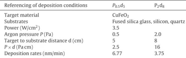
This particular self-organization in two-stacked layers after annealing step was systematically observed for all samples ana-lyzed as shown inFig. 2a and b by SEM and TEM cross section views respectively. XPS and electron probe micro-analysis studies
Fig. 3. GD-OES profiles of a 50 nm thick film deposited at P0,5d5on quartz
sub-strate and annealed in air. Zones 1 and 2 represent the CuO cover layer and the CuO/CuFe2O4heart layer respectively.
revealed that the surface layer consisted of CuO upper layer while the heart layer was composed of CuFe2O4[15]. However these
mea-surements were only performed on 300 nm thick films, and have not been carried out on thinner ones.
Although, GD-OES experiments were realized on 300 and 50 nm thick deposited films. This technique allows us to establish a rapid elemental concentration profiling along the depth of the film/substrate, faster than dynamic secondary ion mass spec-troscopy and the results are more easily quantified [16]. The bilayer structure was observed for both 300 and 50 nm thick films, annealed at 450◦C in air.Fig. 3shows the profile of the different
elements present in the 50 nm thick film. The analytical signal is significantly above the background signal. The three areas iden-tified are consistent with the structure previously revealed by XPS measurements[15]: zones 1 and 2 correspond to the bilayer CuO/CuFe2O4, respectively, and zone 3 to the substrate. Thus,
GD-OES experiments confirm that the CuO/CuFe2O4bi-layer structure
that was only observed previously in the 300 nm thick films is also obtained with our two-step process (deposition/oxidation) on thin-ner sensitive films.
In the case of the composite CuO/BaTiO3, Liao et al.[6]proved
that the elements CuO and BaTiO3taken separately were not
sen-sitive to CO2, whereas the CuO/BaTiO3composite exhibited good
performances. In the other hand, we have already demonstrated
[12]that the CuO/CuFe2O4 bilayer was sensitive to CO2 but the
sensitivity of the single CuFe2O4phase toward this gas was
how-ever nhow-ever checked. We then prepared a CuFe2O4layer by chemical
attack with NH4OH (28%) on the annealed composite bilayer to
dissolve the CuO layer located on top of the copper ferrite layer. Single CuFe2O4 phase characteristic peaks were observed by
X-ray diffraction and Raman spectroscopy (not shown here) after the complete removal of the CuO cover layer by this selective chem-ical etching. Finally, no electrchem-ical measurement could be carried out on the CuFe2O4single layer below 400◦C due to its resistance
which becomes too high. Finally, the original rearrangement of the as-deposited thin film into two layers, during the oxidizing anneal-ing, offers the possibility to detect CO2, whereas the two elements
which are separated are not sensitive to this gas.
This composite material is new and until now no sensing mechanism has been clearly established. It remains quite similar to the CuO–BaTiO3 composite material studied by Herran et al. [5], the most probable assumption is that sensing mechanism of CuO–CuFe2O4 bilayer could be controlled by the work function
variations of p–n heterojunction between CuFe2O4 (n type) and
CuO (p type). Sensing reactions remain to be studied and defined precisely. In our case, the use of dry air in our experiment can lead
Fig. 4. FEG-SEM planar and cross section micrographs of sample annealed (a) 12 h at 450◦C in vacuum and then (b) 12 h at 450◦C in air.
to the formation of iron and/or copper carbonates activated both by oxygen and carbon dioxide. According to research work of Mendayo et al.[17], CO2sensing tests under wet air could lead to an
enhance-ment of the response due to the formation of bicarbonate species concomitantly at the surface of the material. Such experiments will be carried out in a near future.
This specific two-stacked sensitive layers architecture was obtained by a controlled ex situ oxidation process [15] of as-deposited film nanocomposite[13]. In this process, metallic copper and copper (I) species oxidize in copper (II) oxide and diffuse up to the cover layer concomitantly. If the metallic copper particles first migrate to the surface and then, oxidize into CuO in two indepen-dent thermal treatments, this could affect the crystallite size and shape of the active cover layer. According to the literature[18,19], these microstructural characteristics could have an influence on the electrical properties of metal oxides, and then onto the response to CO2. The microstructure of a P0.5d5 as-deposited sample was
then investigated by SEM after an alternative preparation process consisting in two successive annealing treatments under vacuum (12 h at 450◦C) and under air (12 h at 450◦C) instead of a direct
air annealing of the as deposited sample. During the first anneal-ing, metallic copper particles contained in the as-deposited sample migrate to the surface by a phenomenon of coalescence and then, during the second annealing, CuO grains gathered at the surface of CuFe2O4heart layer as shown in SEM micrographs inFig. 4a and
b, respectively. As a result, none electrical measurement could be recorded due to the discontinuity of the CuO upper layer and the highly resistive CuFe2O4 under layer. This confirms that stacking
CuO over CuFe2O4is not a sufficient condition to be CO2sensitive,
microstructure has also a large influence on the sensing properties and our two steps (deposition/oxidation) process play also a great role during the preparation of the bilayer.
3.2. Influence of the thickness
Samples with two different thicknesses have been deposited under low argon pressure and low target-to-substrate distance (P = 0.5 Pa and d = 5 cm, respectively, and called P0.5d5in this work)
in order to compare the response of CuO/CuFe2O4 bilayer within
carbon dioxide atmosphere (5000 ppm CO2).Fig. 5shows the
evo-lution of the response as a function of operating temperature for these two samples with thicknesses set at 50 and 300 nm for the as-deposited samples. We can see that the thinner film presents
Fig. 5. Response evolution (under 5000 ppm CO2) as a function of operating
tem-perature for 50 and 300 nm thick samples.
Table 2
Sensing characteristics of 50 and 300 nm thick samples for 50 and 300 nm thick sam-ples, |R|, t90%and tr90%are response, response time and recovery time, respectively
(tests carried out under 5000 ppm CO2).
Thickness (nm) Toperating(◦C) |R| (%) t90%(min) tr90%(min)
50 250 40 55 8
300 370 15 150 15
both high response of 40% and low optimal operating temperature around 250◦C. In comparison, the 300 nm thick film has an optimal
operating temperature that is shifted to about 350◦C associated to
a strong decrease of the response.
Table 2 gives response (R) and recovery times (t90%) of
these films deposited with two different thicknesses. Both values decrease when the thickness decreases. These results are in good agreement with the literature[9,20].
Seo et al. [21]demonstrated that the control of morphology of the sensing layer is very important to optimize the response char-acteristics of a material. They proposed especially [22]a model that describes the relation between the sensitivity and the gas diffusion. Thus, the sensitivity and response rate tend to increase when the thickness of the sensing layer decreases and its porosity increases. The microstructural characteristics[15]of the sample deposited with P0.5d5 conditions are given inTable 3. Initially,
the as-deposited layer had a thickness of 300 nm. After the heat treatment carried out to oxidize the film, the thickness became 390 nm and the cross-section observation by SEM determined that the thickness of the CuO cover layer was about 120 nm. GD-OES measurements proved that the bilayer structure was conserved in the thinner film. Then, by using a proportionality relationship, we estimated that for the 50 nm thick as-deposited sample, the thick-ness of the copper oxide cover layer after the oxidation step is near 20 nm. The porosity is assumed to stay at a constant value of 40% due to the similar oxidation phenomena of metallic copper during the oxidation phase. According to the sensing mechanism expected, the work-function of p–n heterojunction should change due to the carbonation of the surface. The fastest and the highest CO2response
with a lower operating temperature of the thinnest P0.5d5sample
that has a thinner CuO cover layer (20 nm instead 120 nm for the thicker sample) could be due to a better gas diffusion from sur-rounding atmosphere to the p–n interface through the CuO porous layer. Moreover, the comparison of the SEM view of these samples shows that thinner CuO cover layer has much smaller grains than the thicker one (Fig. 6), which can also lead to an increased response
[23].
3.3. Influence of the deposition conditions
The electric response towards CO2of the P0.5d5sample was in
a second time compared with a new sample elaborated at high argon pressure and high target-to-substrate distance (P = 2.0 Pa and d = 8 cm, respectively, and called P2.0d8in this work). These
exper-imental conditions were chosen because they lead to a different microstructure than that of P0.5d5samples. To compare the
two-stacked architecture with those obtained with P0.5d5 condition,
the microstructural characteristics of the sample deposited with P2.0d8conditions were investigated for an initial as-deposited film
thickness of 300 nm. They are reported inTable 3. However, for the sensing measurements, the as-deposited thickness of this second sample was fixed at 50 nm to enhance the response of the sensi-tive layer according to the results showed previously. The response as a function of operating temperature for the sample P2.0d8had a
trend similar to that seen for the P0.5d5film. Particularly, the
opti-mal temperature was also obtained for an operating temperature close to 250◦C. The sensing characteristics of these two samples,
determined at 250◦C, are compared inTable 4.
The best response is obtained for the sample P0.5d5. Moreover,
response and recovery times are twice shorter in the case of the
Fig. 6. FE-SEM micrographs in-plane view of P0.5d5samples annealed 12 h at 450◦C under air: (a) thickness of the CuO cover layer closed to 120 nm and (b) thickness of the
Table 3
Microstructural characteristics of the samples deposited at P0.5d5and P2.0d8. The total thickness and the thickness of the CuO cover layer for the 50 nm thick samples were
estimated by using a proportionality relationship.
Sample P0.5d5 P2.0d8
Thickness of the as-deposited film 300 nm 50 nm 300 nm 50 nm
Total thickness of the film after 450◦C/12 h air annealing 390 nm 50 × 390/300 = 65 nm (estimated) 310 nm 50 × 310/300 = 52 nm (estimated)
Thickness of the CuO cover layer 120 nm 50 × 120/300 = 20 nm (estimated) 60 nm 50 × 60/300 = 10 nm (estimated)
Porosity of the CuO cover layer 40% <5%
Table 4
Sensing characteristics of the samples deposited at P0.5d5and P2.0d8|R|, t90%and
tr90%are responses, responses times and recovery times respectively (tests carried
out under 5000 ppm CO2).
Sample Toperating(◦C) |R| (%) t90%(min) tr90%(min)
P0.5d5 250 40 55 8
P2.0d8 250 32 100 20
P0.5d5sample than the P2.0d8one. These improvements are linked
to the two-stacked layers microstructures.
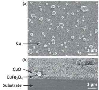
Microstructural characteristics (Table 3) show that the P2.0d8
sample has a CuO cover layer which is dense.Fig. 7exhibits the variation of the porosity of the CuO cover layer as a function of the deposition conditions. In comparison, the P0.5d5sample has a cover
layer which is two times thicker and has a high porosity close to 40%. Using a proportional relationship for a 50 nm thick as-deposited sample, we estimated that after oxidation annealing we obtain, for the P2.0d8sample, a dense CuO layer with a thickness of 10 nm, and
for the P0.5d5condition a 20 nm thick layer of copper oxide highly
porous. The accessibility which is then much better in the case of the latter can then explain the higher response and the lower response time of the sample deposited with P0.5d5conditions.
3.4. Influence of the substrate
XPS measurements were realized on films deposited on con-ventional glass substrate. After annealing in air for long duration at 500◦C, some alkaline elements are supposed to diffuse into the
thin film[24–26].Fig. 8presents a survey scan of a 100 nm P0.5d5
sample after 12 h of air annealing at 500◦C. The spectrum shows
photoelectron lines of a Cu2p, O1s, C1s, Au4f, Na1s and the Auger lines LMM. The presence of gold is due to the electrodes deposited on the surface of the sensing layer for a better electrical contact during the gas sensing tests. The XPS peak of Na observed in the high resolution scan (Fig. 8, inset) imply that sodium migrates from the glass substrate into the thin film. This diffusion of the sodium
Fig. 7. Variation of the porosity in the CuO layer after air annealing as a function of the factor pressure × distance (deposition conditions).
Fig. 8. XPS of 100 nm CuO/CuFe2O4sample deposited on glass substrate Survey scan
and high resolution scan for Na1s inset.
contained in the substrate could have an influence on the sensing response of the composite layer.
In order to avoid the migration of any alkaline element, sen-sitive layers were deposited on quartz substrate with the same sputtering conditions (P0.5d5). As for layers already prepared on
glass substrates, the samples were oxidized at 450◦C for 12 h to
form the CuO/CuFe2O4composite layer and then mounted in the
cell to be tested. Due to the use of this substrate, no alkaline ele-ments could migrate during the annealing step.Fig. 9presents a transient response of the sample under 5000 ppm CO2 with one
hour pulse duration. High and repeatable response values closed to 30% were obtained. However, for 3 h pulse duration which is enough to get the saturated response, we measured a value close to 40% which is similar to the recorded response of the samples deposited on glass substrates. In conclusion, we have not noticed any influence of the sodium diffusion into the sensitive layer.
Fig. 9. Transient response at 250◦C (under 5000 ppm CO
2) for a 50 nm thick sample
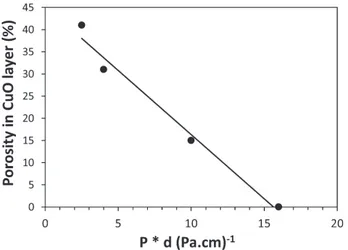
Fig. 10. Response evolution of samples with or without silver additive (t90% is
response time).
3.5. Influence of silver as additive
The presence of additive nanoparticles at the surface or in vol-ume can modify significantly the metal oxide behavior leading to the enhancement of the response towards a gas, as well as to a better gas selectivity[8]. About three nanometers of silver were then sputtered on the surface of a 50 nm P0.5d5deposited sample.
The silver film is too thin to be continuous and then nanometric islands grow on the surface of the bilayer. The size of the silver par-ticles after annealing at 450◦C is difficult to determine and could
not be obtained by FEG-Scanning Electron Microscopy or Atomic Force Microscopy. Due to the temperature used for the sensing test (250◦C) the silver remains at the metallic state[27].Fig. 10shows
that the metallic silver, which cannot be substituted for the cations of iron or copper, improves the response of about 25% compared to a layer without this ultra-thin silver deposition.
Herrán et al.[5]demonstrated that the main physical detec-tion mechanism is based on a work funcdetec-tion variadetec-tion of the p-/n-semiconductor hetero-junction. The introduction of silver as a metallic additive enhances the sensitivity. This phenomenon is explained by a metal/semiconductor junction. Ishihara et al.[28]
also demonstrated that the addition of small amounts of metal or metal oxide onto CuO/BaTiO3was effective in increasing the
sen-sitivity and selectivity to CO2. They especially found that Ag was
the most desirable additive from the standpoint of sensitivity and operating temperature. However the mechanisms remain not clear at the present.
4. Conclusion
Thin films were deposited by RF-sputtering from a CuFeO2
target varying argon pressure and target-to-substrate distance. The sensing layer was obtained after an air annealing for 12 h at 450◦C. Self-organization of the sample after air annealing induced
a p-CuO/n-CuFe2O4 bilayer structure. GD-OES experiments
con-firm that the CuO/CuFe2O4 bi-layer structure is obtained on film
deposited with P0.5d5conditions and for thicknesses of 50 nm
mea-sured in the as-deposited state. This latter film was found to be the sample exhibiting the highest response to 5000 ppm of CO2due to
thin and highly porous CuO upper layer. XPS experiment showed that alkaline element could diffuse from the interface with the con-ventional glass substrate during the oxidation annealing. However, sensing layer deposited on pure quartz substrate could not lead to a higher response to CO2. On the other side, deposition of
sput-tered silver nanoparticles at the surface of the bilayer could improve the response by 25%. These results confirm that nanostructured
CuO/CuFe2O4 bilayers are promising candidates for future cheap
semiconductors CO2 sensors. However, to be fully interesting for
a future industrial application, further additional tests have to be carried out to determine the cross-sensitivity with various gases and the influence of the humidity on the response.
References
[1]T. Ishihara, K. Kometani, M. Hasida, Y. Takita, Application of mixed oxide capac-itor to the selective carbon dioxide sensor, J. Electrochem. Soc. 138 (1991) 173–176.
[2]Y.F. Gu, H.M. Ji, B. Zhang, T.X. Xu, Preparation and CO2gas sensitive properties of CuO–SrTiO3-based semiconductor thin films, Key Eng. Mater. 280-283 (2007) 311–314.
[3]J.C. Xu, G.W. Hunter, D. Lukco, C.C. Liu, B.J. Ward, Novel carbon dioxide microsensor based on tin oxide nanomaterial doped with copper oxide, IEEE Sens. J. 9 (3) (2009) 235–236.
[4]G. Zhang, M. Liu, Effect of particle size and dopant on properties of SnO2-based gas sensors, Sens. Actuators B: Chem. 69 (2000) 144–152.
[5]J. Herrán, G.G. Mandayo, E. Castano, Physical behaviour of BaTiO3–CuO thin-film under carbon dioxide atmospheres, Sens. Actuators B: Chem. 127 (2007) 370–375.
[6]B. Liao, Q. Wei, K. Wang, Y. Liu, Study on CuO–BaTiO3semiconductor CO2sensor, Sens. Actuators B: Chem. 80 (2001) 208–214.
[7]M.I. Baraton, L. Merhari, Determination of the gas sensing potentiality of nano-sized powders by FTIR spectrometry, Scr. Mater. 44 (2001) 1643–1648.
[8]Z. Jiao, F. Chen, R. Su, X. Huang, W. Liu, J. Liu, Study on the characteristics of Ag doped CuO–BaTiO3CO2sensors, Sensors 2 (2002) 366–373.
[9]J. Herrán, G.G. Mandayo, E. Castano, Solid state gas sensor for fast carbon dioxide detection, Sens. Actuators B 129 (2008) 705–709.
[10]J. Herrán, O. Fernandez-Gonzalez, I. Castro-Hurtado, T. Romero, G.G. Mandayo, E. Castano, Photoactivated solid-state gas sensor for carbon dioxide detection at room temperature, Sens. Actuators B 149 (2010) 368–372.
[11]M.I. Baraton, L. Merhari, P. Keller, K. Zweiacker, J.U. Meyer, Novel electronic conductance CO2sensors based on nanocrystalline semiconductors, Mater. Res. Soc. 536 (1999) 341–346.
[12]A. Chapelle, F. Oudrhiri-Hassani, L. Presmanes, A. Barnabé, Ph. Tailhades, CO2 sensing properties of semiconducting copper oxide and spinel ferrite nanocom-posite thin film, Appl. Surf. Sci. 256 (2010) 4715–4719.
[13]A. Chapelle, A. Barnabé, L. Presmanes, Ph. Tailhades, Copper and iron based thin film nanocomposites prepared by radio frequency sputtering. Part I: elaboration and characterization of metal/oxide thin film nanocompos-ites using controlled in situ reduction process, J. Mater. Sci. 48 (2013) 3386–3394.
[14]Th. Neils, M. Aeberhard, M. Hohl, L. Rohr, J. Michler, Characterisation of a pulsed RF-glow discharge in view of its use in OES, J. Anal. At. Spectrom. 21 (2006) 112–125.
[15]A. Barnabé, A. Chapelle, L. Presmanes, Ph. Tailhades, Copper and iron based thin film nanocomposites prepared by radio frequency sputtering., Part II: elab-oration and characterization of oxide/oxide thin film nanocomposites using controlled ex-situ oxidation process, J. Mat. Sci. 48 (2013) 3304–3314.
[16]T. Nelis, J. Pallosi, Glow Discharge as a Tool for Surface and Interface Analysis, Applied Spectroscopy Reviews (2006) 227–258.
[17]G. Mandayo, J. Herran, I. Castro-Hurtado, E. Casta ˜no, Performance of a CO2 impedimetric sensor prototype for air quality monitoring, Sensors 11 (2011) 5047–5057.
[18]N. Murakami, K. Tanaka, K. Sasaki, K. Ihokura, The influence of sintering temper-ature on the characteristics of tin dioxide combustion monitor sensors, Anal. Chem. 17 (1983) 165–170.
[19]X. Wang, S.S. Yee, W.P. Carey, Transition between neck-controlled and grain-boundary-controlled sensitivity of metal-oxide gas sensors, Sens. Actuators B: Chem. 25 (1–3) (1995) 454–457.
[20]N. Yamazoe, G. Sakai, K. Shimanoe, Oxide semiconductor gas sensors, Catal. Surv. Asia 7 (2003) 63–75.
[21]M.H. Seo, M. Yuasa, T. Kida, J.S. Huh, K. Shimanoe, N. Yamazoe, Gas sensing characteristics and porosity control of nanostructured films composed of TiO2 nanotubes, Sens. Actuators B 137 (2009) 513–520.
[22]G. Sakai, N. Matsunaga, K. Shimanoe, N. Yamazoe, Theory of gas-diffusion con-trolled sensitivity for thin film semiconductor gas sensor, Sens. Actuators B 80 (2001) 125–131.
[23]G. Korotcenkov, Gas response control through structural and chemical modifi-cation of metal oxide films: state of the art and approaches, Sens. Actuators B 107 (2005) 209–232.
[24]C. Lim, D.E. Day, Sodium diffusion in glass: II. Mixed sodium–potassium silicate glasses, J. Am. Ceram. Soc. 60 (1977) 473–477.
[25]A. Kolitsch, R. Kuechler, E. Richter, W. Hinz, Tracer diffusion in sodium sili-cate glasses. I. Studies on sodium self-diffusion, Silikattechnik 29 (10) (1978) 302–304.
[26]R. Hempelmann, C.J. Carlile, D. Beyer, Ch. Kaps, Sodium self-diffusion coefficient in sodium silicate glass by quasielastic neutron scattering, Z. Phys. B 95 (1994) 49–53.
[27]K. Kiryukhina, H. Le Trong, Ph. Tailhades, J. Lacaze, V. Baco, M. Gougeon, F. Courtade, S. Dareys, O. Vendier, L. Raynaud, Silver oxalate-based solders: New
materials for high thermal conductivity Microjoining, Scripta Materialia 68 (2013) 623–626.
[28]T. Ishihara, K. Kometani, Y. Nishi, Y. Takita, Improved sensitivity of CuO–BaTiO3 capacitive-type CO2sensor by additives, Sens. Actuators B 28 (1995) 49–54.
Biographies
A. Chapelle received her MSc in materials for energy storage and conversion from University Paul Sabatier of Toulouse in 2008. She obtained her PhD degree in 2012 from CIRIMAT laboratory, Toulouse, France. Her research is now focused on metal oxide sensors in LAAS-CNRS laboratory, Toulouse, France.
I. El Younsi obtained her master’s degree in materials engineering: thin metal layers from University of Strasbourg in 2012. She is currently pursuing her PhD degree on preparation and characterization of new sensitive layers for CO2gas sensors in
CIRIMAT laboratory at Paul Sabatier University, Toulouse, France.
S. Vitale obtained her MSc in materials chemistry at the University of Catania (Italy) in 2011. She has worked for two years (2012–2013) at the Bern University of Applied Sciences (Switzerland), were she was involved in multilayered materials charac-terization by GDOES. She is currently PhD student at the Department of Chemical Sciences of the University of Catania, in LAMSUN laboratory, where she is working on surface engineering via molecular self-assembly for nanotechnology applications. Y. Thimont is an assistant professor at the CIRIMAT laboratory (Toulouse-France) since September 2013. He received his PhD degree in chemistry of materials at the University de Caen Basse-Normandie (France) in 2009 for YBa2Cu3O7thin films
depositions and characterization. He held a nine month post-doctoral position based on the study and the deposition of TCO thin films at the LRCS laboratory (Amiens-France). He then returns to Caen as temporary teacher and researcher in superconductor thematic for two years then held another post-doctoral posi-tion at Caen for one year which devoted to the synthesis and characterizaposi-tion of
thermoelectric silicides. His research interests include the thin films synthesis and topographic, electrical, magnetic and optical characterizations.
T. Nelis received his PhD degree for work on free radical spectroscopy in Bonn, Germany. Since then he has worked several years for major scientific instrument manufactures in the field of glow discharge emission spectroscopy. Since 2011, he is professor for physics at the Bern University of Applied Sciences in Biel Switzerland. His current field of research is plasma processes for thin film deposition and surface modification.
L. Presmanes received his PhD degree, for his thesis-work on ferrite thin films for magneto-optical storage. Since 1997, he has been working in CIRIMAT labo-ratory at University Paul Sabatier (Toulouse) and he is also CNRS researcher since 2001. His research interests are focused on the preparation of sputtered oxide and nano-composites thin films and the study of their microstructure as well as their electrical, magnetic and optical properties. He developed sputtered ferrite thin films to be integrated as sensitive layers in magneto-optical disks and micro-bolometers (IR sensors). His work is currently focused on transparent conducting oxides and semiconductor sensitive layers for gas sensors.
A. Barnabé is a professor at the CIRIMAT laboratory, Paul Sabatier University, France. He received his PhD degree in chemistry of materials from University de Caen-Basse Normandie (France) in 1999. He held a post-doctoral position in Northwestern Uni-versity, Evanston (USA), in 2000. His current research interests are mainly focused in functional metal oxide powders, ceramics and thin films prepared by PVD technique. P. Tailhades received his PhD degree in material science in 1988 and the Habilitation à Diriger les Recherches in 1994. He is currently the vice director of the Centre Interuniversitaire de Recherche et d’Ingénierie des Matériaux (CIRIMAT), Toulouse, France. His research interests include the preparation of original metallic oxides, especially spinel ferrites, in the form of fine powders, thin films, or bulk ceramics and the study of their magnetic, electric, and optical properties. He also works on the preparation of special metallic powders. He received the silver medal of CNRS in France in 2000.