THÈSE
THÈSE
En vue de l’obtention du
DOCTORAT DE L’UNIVERSITÉ DE TOULOUSE
Délivré par : l’Université Toulouse Paul Sabatier (UT Paul Sabatier)
Présentée et soutenue le / / par :
Peter R. Wiecha
Linear and Nonlinear Optical Properties of High Refractive Index Dielectric Nanostructures
JURY
D . N BONOD CNRS, Institut Fresnel, Marseille
P . Ré CARMINATI ESPCI, Paris-Tech, Institut Langevin, Paris P . Gé COLAS DES FRANCS Université de Bourgogne, ICB, Dijon
D . B URBASZEK CNRS, LPCNO, INSA, Toulouse
P . A MLAYAH Université Paul Sabatier, CEMES, Toulouse
D . A é LECESTRE CNRS, LAAS, INP, Toulouse
École doctorale et spécialité :
SDM : Nano-physique, nano-composants, nano-mesures - COP Unité de Recherche :
Centre d’Elaboration de Matériaux et d’Etudes Structurales (UPR ) Directeur(s) de hèse :
Prof. Vincent PAILLARD et Dr. Arnaud ARBOUET Rapporteurs :
c by Peter R. Wiecha typeset with XƎLATEX
Acknowledgements
Initially, I want to thank the French education ministry “ministère de l’éducation nationale, de l’enseignement supérieur et de la recherche” for granting me funding for my PhD thesis. I also thank the directors of the CEMES, Dr. Alain Claverie, et depuis in Dr. Etienne Snoeck, for the opportunity to work in the laboratory and for ensuring a most pleasant working atmosphere. hen, irst of all, I thank my co-supervisor Prof. Vincent Paillard who was always available for any kind of concerns and countless interesting discussions. hanks to Vincent, the last three years were not only fruitful in terms of scientiic productivity but also very enriching in a human way. hank you for your support in truly every respect.
Since typeseting is a strictly sequential mater, I unfortunately have to decide on an order in this acknowledgement. However, I would equally like to thank my second co-supervisor Dr. Arnaud Arbouet. I am grateful for the opportunity to work on his “FEMTO” setup and for his trust when I started tinkering around with all the expensive equipment. I want to express my special gratitude also for the permanent availability concerning any kind of discussions – either scientiic or personal related – for many inspiring ideas, the establishing of many contacts with other researchers and for his priceless eforts in helping me with job applications.
I would also very much like to thank Dr. Christian Girard for his countless stimulating ideas and explanations and particularly for his friendly and very motivating support. hank you also for your availability and for unhesitatingly sharing valuable pieces of code.
Furthermore, thank you Dr. Aurélien Cuche, for leting me participate in the interesting alu-minum thermo-plasmonics project and for very helpful hints concerning optical setups and align-ment.
My thankfulness goes also to Dr. Guilhem Larrieu and Dr. Aurélie Lecestre from LAAS/CNRS in Toulouse, who fabricated the beautiful silicon nano-structures by electron-beam lithography. hank you for the patience and perseverance to do several iterations of fabrication in order to obtain the best possible samples.
In the hope to not forget too many persons, I want to thank furthermore
• Prof. Gerard Colas des Francs for his help and explanations on simulations by the Green Dyadic Method. Particularly I want to express my gratitude for sharing his D GDM code. • Prof. Oto Muskens from Southampton for the fruitful collaboration on several projects
with plasmonic antennas
• Dr. hierry Baron from LTM-CNRS in Grenoble for the VLS grown SiNWs. • Dr. Frank Fournel from CEA/LETI in Grenoble for the SOQ and SOI substrates. • Dr. Houssem Kallel for many precious explanations in the irst months of my thesis. • Prof. Adnen Mlayah for his support and many interesting discussions.
• Leo for the fruitful cooperation and funny nights in Toulouse
• Gonzague for leting me use the sample preparation room including the microscope and for entertaining company in the lab when we were trying SHG from liquid crystals
• Robin, Philippe, Luis and Giuseppe for assisting me with the scanning electron microscope. • Victor for a precious piece of SOI substrate.
• My m’bares Alessandro and Giuseppe, who taught me about south Italian culture and lan-guage and eventually became my Sicilian family. hanks to you it was never boring in the oice.
• Chloé for convincing me to run the PhD student association for one year, and
• Delphine and Audrey for managing this association with me. I won’t forget siting on the back row of Delphine’s car, petriied by her intrepid driving style8
• And inally homas, Nico and Aurélie for taking over the burden of this association. • All the other PhD students of the CEMES for making the last three years so pleasant. I would absolutely mention the legions of open source developers from around the world who, in their vast majority, voluntarily create powerful sotware environments, which are not subject to any proprietary restrictions. Some selected examples are the GNU project, the Latex project or the Python sotware foundation including libraries such as numpy/scipy and matplotlib.
Finally I would like to thank my friends for providing the urgently required distraction from work. hank you David, Manu, Holger, Andisepp, my friends from the Kauferinger Chaos-Trupp (your visit in Toulouse will remain unforgoten), Johannes, Simon, Anna, Sören, Marie, Markus, Flolo, Irene and all the others, I unforgivably have forgoten at this point.
At last I want to thank my family for their support – not only over the last couple of years. I want to thank my Dad for proof-reading the French parts of this thesis. And I deeply thank in particular Cristina for her patience during the last months, and our sons Simon and Oscar, who oten had to wait until late at night for my return from work, for their cheering, carefree happiness.
Contents
Abstract . . . xi Introduction and Motivation . . . .
. Nano-Optics . . . . . . Plasmonics . . . . . . Photonic Particles from High-Index Dielectric Materials . . . . . . . Individual Structures . . . . . . . Dielectric Metamaterials . . . . . . . Beyond Optics . . . . . . High-Index Dielectric vs. Plasmonic Nanostructures . . . . . . . Fabrication . . . . . . . Losses . . . . . . . Electric Field Enhancement . . . . . . . Magnetic Field Enhancement . . . . . . . Scatering . . . . . . Hybrid Plasmonic-Dielectric Nanostructures . . . . . Nonlinear Efects . . . . . . Nonlinear Plasmonics . . . . . . Nonlinear Efects in Dielectric Nanostructures . . . . . . . SHG from Non-Centrosymmetric Materials . . . . . . . SHG from Centrosymmetric Materials . . . . . . Hybrid Plasmonic/Dielectric Structures . . . . . . Applications . . . . . Scope of this Work . . . . Modeling Optical Efects at the Nanoscale . . . . . Deinition of the Problem . . . . . Electrodynamics . . . . . . Maxwell’s Equations . . . . . . Dielectric Permitivity . . . . . . . Metals . . . . . . . Dielectrics . . . . . . uasistatic Approximation . . . . . . Problems Including Retardation Efects . . . . . . . Time Harmonic Fields in Phasor Representation . . . . . . . Wave Equation . . . . . . Green’s Functions . . . . . . Green’s Function for the Electromagnetic Wave Equation . . . .
. . Dyadic Green’s Function . . . . . Green Dyadic Method . . . . . . Lippmann-Schwinger Equation . . . . . . Field Susceptibility for a Homogeneous Environment . . . . . . . Objects in Multi-Layer Environments . . . . . . . Periodic Structures . . . . . . . Two-Dimensional Problems . . . . . . Volume Discretization . . . . . . . Renormalization of Greens Dyadic Function . . . . . . . Paraxial Fields . . . . . . . Tight Focus Correction of the Paraxial Gaussian . . . . . . . Raster-Scan Simulations . . . . . . Resolution of the Inversion Problem . . . . . . . Conjugate Gradients . . . . . . . Preconditioning . . . . . . . Recycling of the Preconditioner . . . . . . Comparison to other Numerical Methods . . . . . . Post-Processing: Analysis of the GDM Results . . . . . . . Electric Nearield Outside the Nanostructure . . . . . . . Magnetic Nearield . . . . . . . Extinction Spectra from the Nearield in a Nanostructure . . . . . . . Farield Patern of the Scatered Light . . . . . Nonlinear Optics . . . . . . Expansion of the Electric Polarization . . . . . . . Symmetric Potentials: Odd-Order Nonlinearities . . . . . . . Asymmetric Potentials: Even-Order Nonlinearities . . . . . . Second Harmonic Generation . . . . . . . Phase-matching . . . . . . . Surface SHG . . . . . . . Bulk Contributions to Surface-SHG . . . . . . SHG in the GDM . . . . . . . Second Harmonic Surface Nonlinear Polarization . . . . . . . Bulk Contributions to Surface SHG . . . . . . . Self-Consistent Nonlinear Polarization . . . . . . Examples . . . . . . . Surface Vectors . . . . . . . Self-Consistent SHG . . . . . . . Conclusions . . . . SHG from Individual Silicon Nanowires . . . . . Linear Optical Response . . . . . . Leaky Mode Resonances . . . . . . Scatering and Absorption . . . . . . Nearield Enhancement . . . . . . Directional Scatering . . . .
. . Inluence of Diferent Geometrical Cross Sections . . . . . . Inluence of a Substrate . . . . . . Nanowires of Finite Length . . . . . Sample and Experimental Setup . . . . . . VLS Grown Silicon Nanowires . . . . . . Nonlinear Microscopy Setup . . . . . Enhanced Nonlinear Optical Response . . . . . . Spectrum of Nonlinear Response . . . . . . Involved Nonlinear Efects . . . . . . . Proile Width of Line-Scans . . . . . . . Power Dependence . . . . . . . Autocorrelation Measurements . . . . . . . Coherent and Incoherent Nonlinear Processes . . . . . . . Conclusions on Involved Nonlinear Processes . . . . . . Second Harmonic Generation Microscopy . . . . . . . SHG Line-Scans along SiNWs . . . . . . . Nearield and SHG Rasterscan Simulations . . . . . . . SHG and Resonant Modes . . . . . . . Comparison of SHG from SiNWs to bulk Materials . . . . . . Conclusions . . . . . Origin of Second Harmonic Generation . . . . . . Introduction: Contributions to Surface SHG . . . . . . Experimental Results . . . . . . heoretical Considerations . . . . . . . Local Surface Contributions . . . . . . . Non-Local Bulk Contributions . . . . . . . Conclusions . . . . . . Simulations . . . . . . . Simulation Method and Model . . . . . . . P(2)
⊥⊥⊥Surface contribution . . . .
. . . Diameter-dependence of SHG contributions . . . . . . . Maps of SHG Farield Intensity Distribution . . . . . . . Eiciency of SHG Epi-Collection . . . . . . Conclusions . . . . Design of Photonic Nanostructures by Evolutionary Optimization . . . . . Design of Nanostructures as Optimization Problem . . . . . . Evolutionary Optimization . . . . . Maximization of SHG from Si Nanoparticles . . . . . . Numerical and Experimental Methods . . . . . . . Structure Model . . . . . . . E-Beam Lithography on SOI . . . . . . . SHG Modeling and Measurement . . . . . . Results and Discussion . . . .
. Optimization of Plasmonic Antennas: Directional Scatering . . . . . . Problem and Model . . . . . . . Model: Cubic Gold Blocks on Substrate . . . . . . . Problem: Directional Scatering . . . . . . Results and Discussion . . . . . . . Analysis of Evolution . . . . . . . Analysis of Optimum Antenna . . . . . . Conclusions . . . . . Multi-Objective Optimization of High-Index Dielectric Particles . . . . . . Optimization Problem and Techniques . . . . . . . Optimizing the Scatering Eiciency from Nanostructures . . . . . . . Evolutionary Multi-Objective Optimization . . . . . . . EMO-GDM Interfacing . . . . . . . Structure Model . . . . . . . Measurements by Confocal Dark-Field Microscopy . . . . . . Results and Discussion . . . . . . . Proof of Principle: λX = λY = 630 nm . . . . . . . Doubly Resonant Nanostructures by EMO-GDM . . . . . . . Polarization Encoded Micro Images . . . . . . . Tuning the Resonances of Silicon Nanoantennas . . . . . . Conclusions . . . . . Conclusions . . . . Conclusion . . . . French Summary / Résumé Français . . . . . Introduction et Motivation . . . . . . Diélectriques à Haut Indice vs. Plasmonique . . . . . . . Plasmonique . . . . . . . Nanostructures de Diélectriques à Haut Indice . . . . . . . Comparaison des Plates-Formes . . . . . . Efets Non-Linéaires . . . . . . . Efets Non-Linéaires dans des Nano-Structures Diélectriques . . . . . . Simulations Numériques de Phénomènes Nano-Optiques . . . . . . Description de la Réponse Linéaire . . . . . . . Déinition du Problème . . . . . . . Méthode Dyadique de Green . . . . . . . Traitement des Résultats . . . . . . Optique Non-Linéaire . . . . . . . Génération de Seconde Harmonique de Surface . . . . . . . SHG avec la GDM . . . . . Réponse Optique Non-Linéaire de Nanoils de Silicium . . . . . . Réponse Linéaire . . . . . . Réponse Non-Linéaire . . . . . . . Échantillons: Nanoils crû par VLS . . . .
. . . Dispositif du Microscope Non-Linéaire . . . . . . . Spectres de l’Émission Non-Linéaire . . . . . . . Dépendance de SHG sur Résonances Optiques . . . . . . . Origine de la SHG . . . . . Optimisation Évolutionniste de Nano-Structures Photoniques . . . . . . Algorithmes d’Optimisation Évolutionniste . . . . . . Optimisation de Nano-Antenne Directionnelle . . . . . . Optimisation de Pixels Double-Résonants . . . . . . Conclusions . . . . APPENDIX
A Dielectric Interfaces . . . . A. Continuity Conditions . . . . A. Relected Field Amplitudes . . . . B Autocorrelation Measurements . . . . B. Model Assuming Unchirped Gaussian Wave Packets . . . . B. . Inluence of Chirp on Gaussian Model . . . . B. Power Series on LiNbO3 . . . .
B. Pulse Width Characterization Using LiNbO3Reference . . . .
C SiNW Surface SHG Polarization Dependence . . . . D SHG from Lithographic Silicon Wires . . . . E Symbols and Abbreviations . . . . List of Figures / List of Tables . . . . Index . . . . List of Publications . . . . Bibliography . . . .
Abstract
Nano-photonic structures ofer a highly interesting platform to enhance light-mater interaction on a nanometer scale. Recently, high-index dielectric structures have gained increasing atention as possible low-loss alternatives to plasmonic nano-antennas made from noble metals. Further-more, since non-linear efects ofer many unique functionalities like the coherent up-conversion of photons, including the generation of harmonics, many eforts are being made to exploit such phenomena in nano-photonics. In this thesis, an analysis is presented on nonlinear optical efects in individual dielectric structures, speciically in silicon nanowires (SiNWs). Nanowires develop strong optical resonances in the visible and infrared spectral range. In this context, strong en-hancement of the optical near-ield together with a large surface to volume ratio support the appearance of nonlinear efects. We show that, compared to bulk Si, a two orders of magnitude increase in second harmonic generation (SHG) is feasible and furthermore unravel diferent po-larization and size-dependent contributions at the origin of the SHG. Numerical simulations are carried out to reairm these experimental indings for which a numerical technique is presented to describe nonlinear efects on the basis of the Green Dyadic Method (GDM). In the last part of the thesis, the GDM is used together with evolutionary optimization (EO) algorithms to tailor and optimize optical properties of photonic nano-structures. We eventually fabricate samples, based on EO design, and successfully verify the predictions of the optimization algorithm. It turns out that EO is an extremely versatile tool and has a tremendous potential for many kinds of further applications in nano-optics.
Résumé
La nano-optique est un vaste domaine permetant d’étudier et d’exalter l’interaction lumière-matière à l’échelle nanométrique. Ce domaine couvre notamment la plasmonique, mais depuis quelques années, un efort est porté sur les nanostructures diélectriques à fort indice de réfrac-tion (typiquement des semiconducteurs comme le silicium). Des efets similaires aux nanopar-ticules plasmoniques peuvent être obtenus, tels un comportement d’antenne et l’exaltation de phénomènes non linéaires (génération d’harmoniques), avec l’avantage de faibles pertes. Dans cete thèse, une analyse des propriétés optiques linéaires et non linéaires de nanostructures in-dividuelles. Une première partie est dédiée aux nanoils de silicium qui supportent de fortes résonances optiques dont le nombre et la gamme spectrale, du proche UV au proche IR, sont fonction de leur diamètre. Dans ces conditions, l’exaltation du champ proche optique et un rap-port surface sur volume élevé favorisent l’apparition de processus non linéaires. Ainsi la généra-tion de seconde harmonique (SHG) par rapport au silicium massif est augmentée de deux ordres de grandeur. En outre, diférentes contributions à l’origine de la SHG peuvent être adressées individuellement en fonction de la polarisation du laser d’excitation et de la taille des nanoils. Les résultats expérimentaux sont confrontés à des simulations numériques (méthode dyadique de Green, GDM), qui permetent d’identiier les diférentes contributions. Dans une seconde partie, la méthode dyadique de Green est couplée à des algorithme évolutionnistes (EO) pour la conception et l’optimisation de propriétés optiques choisies de nanostructures semiconduc-trices ou métalliques, par exemple difusion résonnante de diférentes longueurs d’ondes pour diférentes polarisations. Des échantillons de nanostructures de silicium, réalisés à partir des ré-sultats de l’EO, vériient avec succès les prédictions de l’algorithme d’optimisation, démontrant l’énorme potentiel de l’EO pour de nombreuses applications en nanophotonique requérant une optimisation simultanée de diférents paramètres.
Chapter
Introduction and Motivation
. Nano-Optics
N
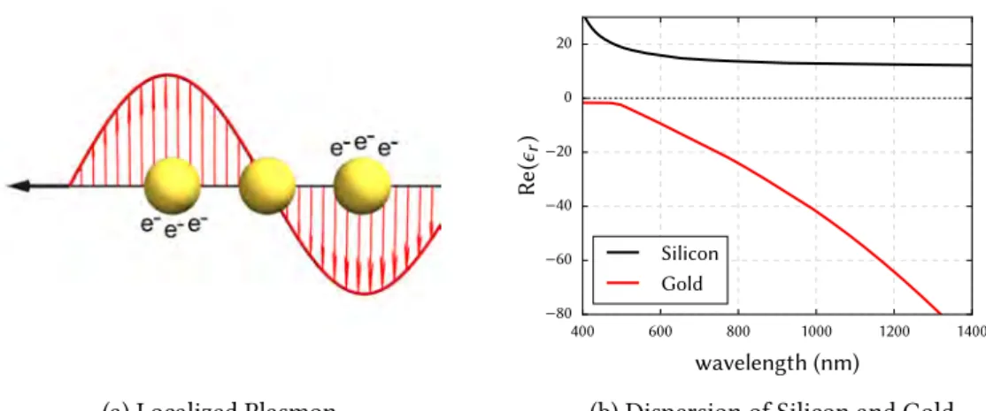
- is a ield which is increasingly drawing atention of researchers worldwide. In general, nano-optics is the research ield on efects of light-mater interaction occur-ring at subwavelength dimensions – thus at the nanometer scale for visible and near-infrared light. Usually, all phenomena can be described by classical electrodynamics, i.e. by the set of Maxwell’s equations [ ]. In this chapter we give an overview of diferent material sys-tems and of the current research progress on photonic nano-structures and their applications. A comparison between plasmonic structures and high-index dielectric antennas motivates more profound investigations on the later material system. Finally we give a brief review on nonlinear efects in nano-optics.. . Plasmonics
One of the main driving forces in nano-optics is the ield of plasmonics [ , ]. Interaction of electromagnetic waves with metals can launch collective oscillations of free electrons from the conduction band. he dielectric constant of metals is negative (see Fig. . b), leading to an imag-inary wavevector. Fields are therefore evanescent and conined within a small region at the sur-face, called “skin-depth” [ ]. In consequence, collection oscillations of the electrons propagate along the surface and are called surface plasmon polaritons (SPP) [ – ]. In small metal particles, the propagation of SPPs is hindered due to the spatial coninement and localized modes appear, so-called localized surface plasmon (LSP) resonances (see Fig. . a). For an extensive introduc-tion on plasmonics, we refer the reader to reference [ ]. hese conined plasmon oscillaintroduc-tions allow to squeeze light into tiny volumes of subwavelength size, far below the difraction limit and yield extremely high local ield enhancements [ ]. In the visible spectral range this results in characteristic sizes of several tenths to a few hundreds of nanometers. Such plasmonic particles are oten referred to as “optical antennas” [ – ].
A multitude of designs for such antennas have been proposed for various purposes. It is for example possible to obtain spectrally well deined resonances which may be used for color-iltering and -rendering or printing at the difraction limit [ – ] or, on the other hand, to create broadband antennas [ ]. Other designs allow either polarization-sensitivity or -insensitivity [ , , ] and polarization conversion [ , ]. Furthermore it is possible to create interfer-ences between modes resulting in Fano-like resonances [ ] or enhancement of higher mul-tipolar radiative transitions that would usually be too weak for observation [ ]. Also chiral responses can be tailored to react sensitive to let- or right-circular polarized light [ – ]. Another example is strong directivity in the scatered angular intensity distribution that can
(a) Localized Plasmon 400 600 800 1000 1200 1400 wavelength (nm) −80 −60 −40 −20 0 20 Re (ϵr ) Silicon Gold
(b) Dispersion of Silicon and Gold
Figure . : (a) sketch of localized surface plasmons in gold nanospheres induced by an electromagnetic ield and (b) real part of the relative permitivity of gold and silicon.
for example be achieved with antenna arrangements similar to radio-frequency antennas [ – ]. Also forward/backward anisotropic scatering can be obtained [ ] and even the possibil-ity of wavelength-dependent switching of directionalpossibil-ity has been reported [ ]. Larger two-dimensional antennas pronounce higher order spatial modes with complex, tailorable ield dis-tributions that can be resolved for example using two-photon luminescence (TPL) [ – ] or electron energy loss spectroscopy (EELS) techniques [ ]. Acoustic vibrations can be optically excited in nano-antennas, that have been used as nano-sources for hypersound generation [ ,
].
Applications range from signal processing [ , ] over surface enhanced spectroscopies where strong plasmonic ield enhancements are exploited to boost signals from few or even single molecules, from weak luorescent transitions or from molecular vibrations [ , – ] to biomedical applications in which plasmonic particles are used as nano-biosensors for speciic biomolecules [ ], as biomarkers [ , ] or for local thermal treatment [ , ] and drug deliv-ery [ ]. Sharp resonances can be used for tuning [ ] and sensing [ , ] in optomechanical plasmonic resonators.
. . Photonic Particles from High-Index Dielectric Materials
he main focus of this work will be put on another type of photonic nanostructures, namely high-refractive index dielectric nanoparticles. Usually, the later materials comprise semiconductors such as germanium or silicon (Si refractive index in the visible n ≈ 3.5 - 4). he decisive diference to plasmonics is the lack of free carriers. his results in a positive real part of the dielectric function (see Fig. . b) which means that light can actually propagate inside the material. Under electric ields, the material is polarized due to a displacement of the bound carriers relative to their latice atoms and this polarization is proportional to the dielectric contrast with the environment (see also appendix . . ).
accessi-ble also from high-index dielectric nanostructures – with the advantage of very low absorptive losses [ , ].
. . . Individual Structures
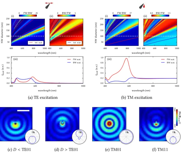
In the early ’s, the possibility to use horizontal silicon nanowires (SiNWs) as antennas for vis-ible light was irst exploited in the context of enhanced absorption [ ] and Raman spectroscopy [ ]. By simply changing the diameter, optical resonances can be tuned all over the UV and visi-ble spectrum up to the infrared [ , ]. An optical darkield microscopy image of diferent large NWs is shown in Fig. . a, where the size-dependent redshit of the resonance wavelength is clearly visible. It was then shown, that also the material composition is a convenient parameter for tuning the resonance positions [ ]. In nanowires, these resonances are strongly polarization dependent, as is their nearield distribution [ ], a property that can be used for polarization il-ters [ ] or to obtain spectrally enhanced and strongly polarized photoluminescence from direct bandgap semiconductor NWs [ ]. A multitude of structures has been studied in the meantime, such as low aspect ratio [ , ] and vertical nanowires [ ], nanospheres [ ], nanodiscs [ ], hollow nanocylinders [ ] coupled dimers [ – ] or even complex bio-inspired structures [ ]. Also heterostructures composed of mixed materials have been investigated [ ]. For example the absorption eiciency of NWs could be increased signiicantly by using amorphous-/crystalline-Si [ ] or Ge/Si core/shell structures [ ].
Similar functionalities as with plasmonic antennas have been realized on the high-index di-electrics platform. Guiding light for all-optical signal processing is a commercially established application of silicon nanostructures [ , ] and eforts are being made to couple other dielec-tric materials to the CMOS platform [ ]. Nanowires are also used to guide single photons or entangled photon pairs e.g. for quantum computing [ ]. Apart from wave-guiding, numer-ous other possible applications exist. he possibility to obtain well deined optical resonances in high-index nanowires can be used to create single-NW lasers [ ] and achieve mode-iltered lasing from such individual NWs [ ]. Recently an optical diode for circularly polarized light has been proposed [ ] which is a step towards all-optical logical elements. It is also possible to create forwards/backwards selective uni-directional scatering [ – ] or even scatering to-wards arbitrary angles [ ] by taking advantage of interferences between degenerate resonance modes. he aforementioned possibility to tune the resonance wavelengths is similarly lexible as in plasmonic antennas and is supposed to be very valuable for solar cell applications [ – ]. It has been also shown, that high-index dielectric nano antennas can be used as alternatives to metal particles in surface enhanced luorescence spectroscopy (SEF) and surface enhanced Raman spectroscopy (SERS) [ ]. While ield-enhancement is several times lower compared to metal antennas, larger ield volumes and by far lower losses may compensate this drawback in many applications [ ].
. . . Dielectric Metamaterials
When individual nano-structures are put together and are arranged orderly on large areas, such surfaces can have very surprising macroscopic optical properties – that, very importantly, are tailorable to individual needs. Such so-called metasurfaces or metamaterials [ ] are oten made of plasmonic elements [ ], but here we will focus on an introduction to all-dielectric metama-terials [ , ].
In direct analogy to the optical properties of individual nanostructures, metasurfaces with spectrally well deined resonances can be designed. In this way, optical band-pass ilters [ ], full-color holograms [ ], highly absorptive surfaces [ ], polarization converters [ ] or, by puting the individual dielectric elements on a lexible substrate, mechanically tunable metamate-rials [ ] have been created. By tuning spectrally the ratio of forward and backward scatering, metasurfaces with particularly high relectance [ – ] or transmitance [ ] have been re-ported, as well as metasurfaces designed for ultra-fast optically induced transparency [ ]. he ability to spatially tune the phase of an incident beam allows wavefront shaping, polarization control e.g. for radially polarized beam generation or focusing from planar structures [ , ]. A generalized Brewster efect can be obtained from surfaces composed of silicon nanospheres which has been used for the tailoring of directional scatering [ ]. Directionality has also been used to vertically couple light from a waveguide to free space, which opens perspectives for ap-plications in optical signal processing [ ]. Even materials can be designed that allow optical cloaking, i.e invisibility of small objects [ ] (for details on cloaking, see [ ] or [ ]).
. . . Beyond Optics
High-index dielectric nanostructures are also promising for possible multi-purpose applications. For instance thermal rectiication in telescopic Si NWs – which basically represent diodes for heat transport – has been demonstrated recently for NWs with diameters ≈ 10 nm [ ]. her-moelectric properties could be enhanced in dielectric metamaterials by artiicially increasing the ratio of electric over heat conductivity [ ]. Another research group used resistance hystere-sis in silicon nanowires with encoded abrupt doping-proiles to implement non-volatile memory [ ]. Such efects could be exploited simultaneously to the unique optical properties of dielectric nanoparticles with manifold imaginable applications.
. . High-Index Dielectric vs. Plasmonic Nanostructures
In the preceding introduction, we focused mainly on the similarities of plasmonic and dielectric materials. Let us now compare the diferences between them in some more detail in order to expose advantages and drawbacks of the two material systems.
. . . Fabrication
We will start with some words on the fabrication of nanostructures. Plasmonic structures con-sist of metals, usually gold, silver or aluminum. hey are either evaporated on a substrate with a subsequent lithographic step and lit-of [ ] or chemically synthesized [ – ]. Colloidal particles have been orderly arranged with DNA origami templates [ ] or larger chemically syn-thesized crystalline lakes can be very rapidly structured by interferometric lithography [ ]. he irst approach sufers from the relatively poor and oten polycrystalline quality of evapo-rated metals whereas the mono-crystalline metal nanoparticles from the later technique usually cannot be up-scaled to obtain large-area substrates.
High-index dielectric materials can also be evaporated or sputered with the same drawbacks that hold for the metal case. Silicon nanowires can be grown by vapor-liquid-solid (VLS) epitaxy, which is a technique that can be easily up-scaled. A key advantage of the VLS-method is that it allows a very accurate deinition of the size and aspect ratio of a large quantity of simultaneously
W= 30nm
W= 400nm
(a) Darkield Image of Silicon NWs
(b) Magnetic Resonances: Au vs. Si (c) Heat Dissipation: Au vs. GaP
Figure . : (a): Darkield image of 5 μm long SOI-etched silicon nanowires with widths from 30 nm at the let to 400 nm at the right. (b) sketch of magnetic ield generation in metal split-ring resonators (let) and dielectric nanospheres (right), reprinted from Kuznetsov et al. [ ]. Copyright ( ) CC BY. (c) comparison of heat dissipation in gold (let) and gallium phosphide dimers (right), adapted with permission from Albella et al. [ ]. Copyright ( ) American Chemical Society.
grown nanowires [ ]. In particular for silicon, another common approach is the lithographic deinition of structures on the crystalline silicon layer on a silicon-on-insulator (SOI) substrate [ , ]. A key advantage in this context is the almost perfect control of structure deinitions thanks to the compatibility to state-of-the art CMOS technology procedures.
. . . Losses
A major disadvantage of plasmonic nanostructures for ield enhanced spectroscopy are the sig-niicant losses associated to the large imaginary part of the dielectric permitivity in metals. hese losses are responsible for signiicant heat generation in the particles which can be lethal for fragile biomolecules. If the emiters survive the heating, their weak signals might be directly re-absorbed by the lossy metal particle, neutralizing the efect of enhanced emission. Although high-index dielectrics yield signiicantly lower ield enhancements, the associated losses are even by several orders of magnitude smaller (see also Fig. . ). For structures of comparable ield en-hancements, the diference in temperature gradients between plasmonic and dielectric particles can reach several 100◦C [ , ] (see Fig. . c).
he very low losses are a key advantage of dielectric materials when it comes to spectroscopy applications. However, the dissipation in plasmonic antennas can be used for localized heat generation at a nanometer scale [ ] which on the other hand is not possible with dielectric nanostructures.
. . . Electric Field Enhancement
Field enhanced spectroscopy is one of the main applications for plasmonic particles. High ield enhancements are necessary in order to boost the weak signals from few or even single molecules. Field enhancement in the vicinity of high-index semiconductor nanoparticles is essentially pro-portional to the dielectric contrast between the particle (ϵr, 1) and its environment (ϵr, 0). his is
a result of the continuity conditions for ields across dielectric interfaces (see appendixA. ) E∥,0= E∥,1 ϵr, 0E⊥,0= ϵr, 1E⊥,1. ( . )
he normal component of the electric ield close to the particle is enhanced by the ratio of the permitivities and possibly further ampliied due to the presence of resonant modes. For many semiconductors, strong ield enhancement in the order of ≈ 100-fold ampliication of the ield intensities are possible (ϵr > 10), where resonant optical modes further increase the efect [ ,
, ] (see Fig. . ). Also a tightly focused excitation can increase the ield enhancement and lower the efective volume of high ield concentration [ ]. he enhancement factors are nev-ertheless signiicantly lower than in plasmonics, where three orders of magnitude in intensity enhancement can easily be achieved [ ]. While in plasmonics generally the strongest nearields can be obtained, dielectric particles ofer larger volumes of ield enhancement [ ], which, under circumstances, can be advantageous. he range of the strongest ield enhancement is in the order of ≈ 1 nm for plasmonic antennas and ≈ 10 nm in dielectric nano-particles. his is in particular advantageous when it comes to the fabrication of nano-particles featuring such small gaps. Re-ported gain in luorescence rate using dielectric particles range from values ≈ 5 [ ] to ≈ 35 [ ].
. . . Magnetic Field Enhancement
Another noteworthy diference are strong magnetic resonances in dielectric nanoparticles, which are hard to obtain in plasmonic antennas [ , – ]. Magnetic dipolar resonances in dielectric dimers can yield an ≈ 100-fold increase of magnetic ield intensities at visible frequencies [ ], similarly strong as the electric ield enhancement. In plasmonics, comparable performances are achievable only with complex asymmetric particle arrangements [ ] or in the infrared using split-ring resonators [ ] (see also Fig. . b). he performance of magnetic ield enhancement generally sufers from strong losses in plasmonic particles in the visible spectral range [ ].
he magnetic resonances in dielectric nanoantennas can be used to tailor the magnetic local density of states [ ]. Furthermore they can lead to behavior similar to magnetic media in actually non-magnetic (µr = 1) media. Because the magnetic resonances can be tuned to be of
comparable strength with the electric resonances, the so-called Kerker-condition (µr = ϵr, [ ])
can be fulilled even in dielectric media where clearly µr , ϵr, leading to strongly directional
scatering [ , , – ].
Apart from the visible spectral range, strong magnetic ields have been demonstrated in high-index dielectric particles also for GHz [ ] and THz frequencies [ ].
. . . Scatering
Finally, despite very strong ield enhancements, scatering to the farield from plasmonic anten-nas is limited [ ] and oten outperformed by their dielectric counterparts [ ], as demonstrated
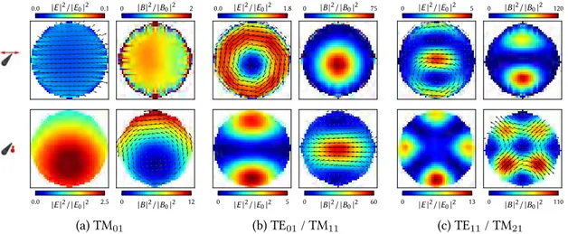
0 2 4 6 8 10 12 Qex t. , Qsc a t. extinction scattering 400 500 600 700 800 900 1000 wavelength (nm) 0 50 100 150 200 |E | 2/ |E0 | 2 0 10 20 30 40 |B |2 / |B 0| 2 E B
(a) R = 80 nm Silicon Dimer
0 2 4 6 8 10 12 Qex t. , Qsc a t. absorptive losses 400 500 600 700 800 900 1000 wavelength (nm) 0 50 100 150 200 |E | 2/ |E0 | 2 0 10 20 30 40 |B |2 / |B 0| 2 (b) R = 40 nm Gold Dimer
Figure . : Extinction and scatering eiciency spectra (top) as well as nearield enhancement (botom: E-ield: red, B-E-ield: blue) in the gap of (a) a dimer of two silicon spheres with radius R = 80 nm and (b) a gold dimer with R = 40 nm. Gap is R/4 in both cases. Sizes were chosen to obtain resonances around λ = 600 nm. Incident planewave polarized along dimer axis. Dimers are placed in vacuum. A sketch of the model and numerical mesh used in the simulations for the gold and silicon dimers is shown above the plots.
by the numerical simulations comparing the scatering eiciencies from gold and silicon dimers, shown in Fig. . . In summary, dielectric antennas may be equal or even favorable alternatives to plasmonic systems, dependent on the targeted application.
. . Hybrid Plasmonic-Dielectric Nanostructures
In many regards, the plasmonic and dielectric platforms ofer complementary properties. It is therefore not surprising, that eforts are being made to bring together both systems into hybrid plasmonic-dielectric nanostructures and combine their mutual advantages.
High-index particles have been used for example as “sensors” for plasmons, coupling propa-gating SPPs on metal surfaces to the farield [ ]. Inversely, metal particles were incorporated in dielectric waveguides to ilter frequencies in the waveguide transmission around the plas-monic particles’ resonance [ ]. In diferent works, the coupling between plasmonic particles and dielectric nanowires was used to circumvent the polarization-anisotropy in scatering from semiconductor nanowires [ , ]. In this context, metal/dielectric nanospheres were pro-posed as “super-scaterers” with remarkably high scatering eiciencies due to superposition of multiple resonances [ ] or inversely “super-absorbers” were designed by decorating sili-con nanowires with plasmonic gold particles [ ]. In quantum dot doped NWs, lasing from sub difraction-limit mode-volumes was realized by coupling to SPPs [ ]. Plasmonic anten-nas were employed to boost photoluminescence from III-V semiconductor nanostructures via strong ield enhancement [ ]. Hybrid waveguides were suggested that ofer spectrally broad high power transmissions and could be promising for scanning-tip microscopy applications like SNOM in order to guide light to few square-nanometer small sample areas [ ]. Concepts to
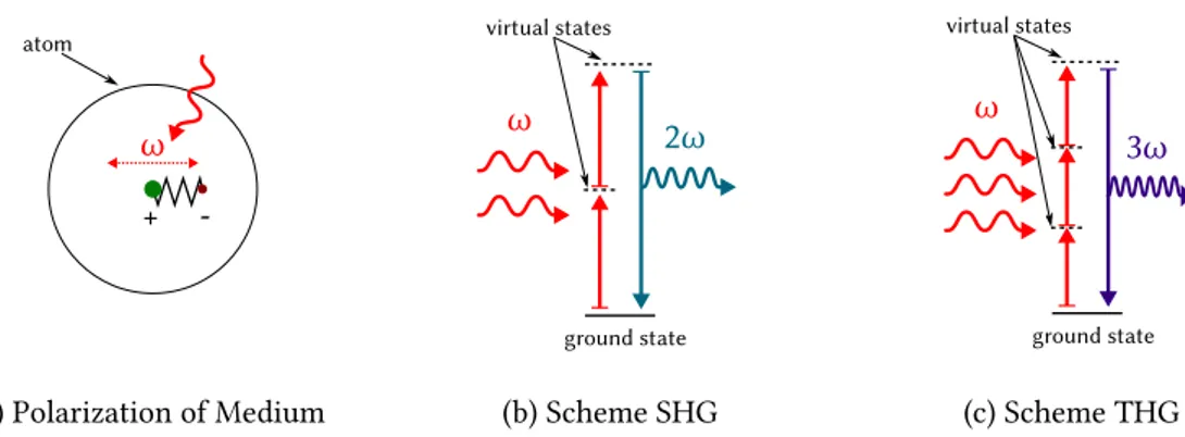
ω 2ω ground state virtual states (a) SHG ω ωTPL ω ground state band edge intermediate states (b) TPL ω 3ω ground state virtual states (c) THG ω1 ground state virtual states ω2 ω3 ω4 (d) FWM
Figure . : Schemes illustrating (a) second harmonic generation, (b) two photon induced photolumines-cence, (c) third harmonic generation and (d) one possible interaction diagram of four-wave mixing.
improve directional emission have also been proposed on the basis of hybrid plasmonics. Com-pared to an all-metal design [ ], enhanced directivity could be achieved using a metal antenna as driving element and a low-loss dielectric antenna as director [ ]. In a similar work the signii-cantly lower losses have been pointed out, using a dielectric component to reduce re-absorption [ ]. Also, diiculties associated with the weak optical magnetism of plasmonic particles can be avoided using mixed metal-dielectric structures [ ]. his might be an important concept if strong magnetic ields are desired in the vicinity of metal structures. Finally, promising appli-cations can also be found in photovoltaics. For example, paterned metal-ilms with embedded silicon nano-pillars showed drastically increased absorption compared to non-paterned ilms, while the low electrical resistance of the metal ilm was maintained [ ].
. Nonlinear Efects
All properties and applications of nano-photonic particles described above were based on a linear optical response. If the amplitude of the exciting electromagnetic ield is high enough, nonlinear optical efects occur, that can ofer a large range of unique functionalities beyond linear op-tics. Probably the most popular nonlinear optical efect is harmonics generation [ ]. Among this, the most prominent examples are second harmonic (SHG, illustrated in Fig. . a) and third harmonic generation (THG, Fig. . c): Two (or three) photons of a fundamental wavelength λ0
are coherently up-converted (i.e. the process happens instantaneously, there are no interme-diate states) to a single photon with λSHG = λ0/2(or λTHG = λ0/3). Apart from harmonics
generation, other widely exploited nonlinear phenomena are: Sum- and diference-frequency generation (not shown), four-wave mixing (FWM, Fig. . d) used for example in optical para-metric oscillators and ampliiers [ , ], or two photon induced photoluminescence (TPL, see Fig. . b), which is an incoherent conversion of two incident photons to one photon of shorter wavelength (with λ0 > λTPL > λ0/2), involving intermediate states with inite lifetimes [ ,
].
he link between nonlinear optics and nano-antennas is the need of high ield amplitudes in the former and the possibility to strongly enhance electric ields in the later. herefore nano-photonic structures seem ideal candidates to evoke nonlinear efects and increasing interest is
being put on nonlinear nano-optics. In this section, we give an overview on current research and on applications of nonlinear efects in nanometric plasmonic and dielectric systems.
. . Nonlinear Plasmonics
Following the outline of the previous section, we will start with some brief examples of current research on nonlinear efects in plasmonics.
In gold, which is a centrosymmetric crystal, second order nonlinear efects such as SHG vanish in the dipolar approximation [ ]. Nevertheless, by breaking the symmetry at the level of the nano-structure design, signiicant SHG can be obtained from gold plasmonic antennas [ ]. It turned out, that SHG can even be further enhanced using multi-resonant antennas with modes at λ0and λ0/2[ – ], but the eiciency of propagation of SHG to the farield remains crucially
dependent on microscopic symmetries [ , ]. It has been shown, that by using a control beam at λ0/2, the directionality and scatering eiciency of SHG can be controlled [ ]. Furthermore,
size dependent polarization efects occur in SHG from nanoparticles, that arise from diferent physical processes at the origin of the nonlinear radiation [ , ]. Equally to SHG, also THG can be heavily enhanced in resonant plasmonic antennas [ ]. Other nonlinear efects like sum-or diference-frequency generation and four-wave mixing can also be enhanced [ , ]. Apart from enhancement of nonlinear processes, the incoherent character of two photon luminescence can be used to image spatial mode distributions in larger two-dimensional plasmonic resonators [ , , , ]. A more extensive overview on nonlinear plasmonics can be found in reviews on this topic, e.g. by Kauranen and Zayats [ ] or by Butet et al. [ ].
Despite all recent progresses in nonlinear plasmonics it has been shown that the eiciency of nonlinear processes in metal nano-particles is inherently limited, mainly due to dissipation processes [ ].
. . Nonlinear Efects in Dielectric Nanostructures
Because of lower losses and other advantages like compatibility to CMOS technology (for sili-con), high-index dielectric structures may also be promising alternatives to nonlinear plasmon-ics. Particularly nonlinear photonics on the silicon platform are subject of current research, with the goal of implementing all-optical signal processing in Si-based microelectronic devices [ ]. hird-order nonlinear efects are very promising in this context, because of the inherently high χ(3) of silicon. his allows enhanced third harmonic generation with factors of up to 105 com-pared to bulk Si using photonic crystals [ ] or dielectric nano-antennas [ – ]. Harmonic light can be produced, intense enough to be visible with the bare human eye [ ].
. . . SHG from Non-Centrosymmetric Materials
Despite the great prospects of third order efects, they can be experimentally inconvenient be-cause the fundamental frequency has to be chosen in the infrared in order to obtain a response in the visible. herefore, second order efects and in particular second harmonic generation (SHG) are subject of current research. In this context, dielectrics with a non-centrosymmetric crystal ofer a great advantage over plasmonics, because SHG can be generated from the bulk crystal itself.
Strong second harmonic light could be for example generated from subwavelength small Al-GaAs cylinders and was found to be enhanced by magnetic Mie resonances [ ]. Using this strong SHG in nonlinear farield-microscopy was used to reveal the spatial paterning of hybrid guided- / Mie-modes (see also [ ]) in GaAs nanowires [ ]. Control on properties of nonlinear efects has also been reported. For example the directionality of the (strongly enhanced) SHG from ZnTe NWs [ ] or AlGaAs nanodiscs [ ] can be controlled by means of the incident beam polarization and the particle’s aspect ratio. Also the polarization of the SH light in the farield could be controlled by modal engineering in GaP nanopillars [ ].
. . . SHG from Centrosymmetric Materials
Elemental silicon is among the experimentally most convenient materials. Unfortunately, like all elemental crystals with face-centered cubic (fcc) latice, bulk Si has an inversion symmetry and therefore doesn’t support second order nonlinear efects in the dipolar approximation.
Nevertheless, second order nonlinear efects and particularly SHG is still of interest in cen-trosymmetric nano-particles. Due to a breaking of the inversion symmetry at interfaces and with large surface-to-volume ratios in small particles, the efective nonlinear susceptibility is actually non-zero. Furthermore, ield-gradients can arise due to tight focusing or resonant optical modes, that also break the symmetry locally and support a second-order nonlinear response. herefore, a lot of theoretical work has been done for SHG from nanoparticles of centrosymmetric materi-als [ – ]. Experimentally, enhancement of SHG has been reported for example from SiNW arrays (> ×50 compared to bulk) [ ]. Also Si photonic crystals can enhance SHG and THG signiicantly, even under cw excitation suiciently strong ields could be obtained to generate measurable second harmonic light. Radiation paterns conirmed in these experiments, that THG is indeed generated within the bulk, while SHG is a surface efect [ ]. As SHG requires a break-ing of the symmetry at some point, strained dielectric slabs have been studied in this context as well. And indeed, a good enhancement of SHG from strained silicon [ , ] or germanium waveguides [ ] was found. However, it has been recently reported that the inluence of strain on the bulk second order susceptibility of silicon had been overestimated earlier [ ].
. . Hybrid Plasmonic/Dielectric Structures
Also in nonlinear nano-optics, atempts are being made to combine advantages of plasmonics and high-index dielectrics. A tremendous increase of THG by a factor of 106could be achieved
by coupling indium-tin-oxide (ITO) to the enhanced nearield of a plasmonic antenna [ ]. In an other work, the eiciency of FWM (Fig. . d) could be increased using a hybrid silicon/plasmonic waveguide [ ].
. . Applications
Probably the best motivation for further investigations on nonlinear properties are the mani-fold possible applications of nonlinear optical efects in nano-structures. he fact that SHG from centrosymmetric crystals is a surface efect is widely exploited for macroscopic surface char-acterization [ – ]. But also on a nanometer scale, characteristic surface signatures can be obtained from SHG spectroscopy. he surface second harmonic light from gallium-nitride (GaN) nanowires for example contains a signature of the surface orientation [ ] or aluminum grain
boundary interfaces can be analyzed by SHG microscopy [ ]. Nonlinear optical efects are also widely used in signal processing based on silicon photonics [ ]. As an example, a passive optical modulator was realized thanks to a strain-induced increase in nonlinearity by one order of magnitude in silicon waveguides [ ]. Also ultrafast all-optical switching can be obtained in silicon nano-structures, making use of a spectral shit of the magnetic dipole resonance caused by two-photon absorption [ ]. Apart from quantum computing, where a lot of efort is put in both linear [ – ] and nonlinear [ ] optical techniques, optical computing might also be done in a more classical way, basing on optical switching. An optical transistor would require some nonlinear optical phenomena in order to achieve a switching behavior. Such a device has been proposed as early as by Jain and Prat Jr. [ ] who suggested that a refractive-index perturbation induced by a “base” beam could be used to nonlinearly control the intensity of SHG from the device by a variation of the phase-matching condition. In this device, the equivalent to the collector would be the fundamental incident beam and the emited SHG would correspond to a transistor’s emiter. More recently, a polarization controlled logical element was proposed using TPL from plasmonic nanostructures supporting higher-order spatial modes [ ].
Equivalently to surface second harmonic generation, SHG is highly sensitive to small changes of the nano-particle geometry, which has been proposed to be exploited for far-ield measure-ments of few nanometer small distances using a kind of optical “nano-ruler” [ ]. Infrared-excited SHG from dielectric GaP nanoparticles has been proposed as femtosecond nanome-ter light source at visible frequencies for applications related to bio-imaging [ ]. In such nano-probes, engineering of the geometry allows to shape the modes and thereby the harmonic nearield as well as its polarization state. In the context of nano-scale localized sensing, it has been shown that a nonlinear response can ofer about one order of magnitude higher sensitivity to changes in the refractive index compared to linear optical refractive index sensing [ ]. An other work-group used cadmium-sulide (CdS) NWs as nanometer scale optical correlators which opens perspectives for on-chip ultrafast optical technologies [ ]. Finally, nonlinear efects can be used in bio-medical applications. SiNWs were used as biomarkers and excited with an infrared fs-laser. he detected THG provides not only the biomarkers’ positions but also information on their orientation due to anisotropic THG as a result from the high aspect ratio of the NWs [ ].
. Scope of this Work
he focus in this work will be put on nonlinear efects in dielectric structures, in particular in silicon nanowires. In the irst part (page and following), the fundamental electro-dynamical theory will be introduced and an introduction to nonlinear optical efects will be given. We will give an overview on the Green dyadic method (GDM), a technique for the numerical modeling of the response of nano-objects to an excitation by electromagnetic ields. In this context, also for nonlinear optical efects a numerical description will be presented and discussed (page and following).
In the second part (page and following), a thorough study of the optical behavior of silicon nanowires (SiNWs) in the visible spectral range will be performed. At irst, the linear optical properties will be discussed. Subsequently the nonlinear optical response will be subject of an experimental and theoretical analysis. Finally, second harmonic generation (SHG) will be exam-ined in detail and we will ind, that the origin of the frequency doubling in SiNWs depends on the polarization of the fundamental ield as well as on the size of the nanowires, which opens
interesting perspectives for further studies of surface SHG from nanowires or for applications which require control of the harmonic emission.
In the last part (page and following), we will discuss the more technological problem of nanostructure design. As described above, optical properties of photonic nanostructures can be tailored to speciic needs. For this, usually some reference design is chosen by intuitive con-siderations. By a systematic analysis of the system, the desired properties are maximized sub-sequently. However, inding optimum geometries for a given problem is not trivial, and oten trade-ofs have to be made. We therefore tackle the problem in an inverse way: Ater deining the desired optical properties, a corresponding geometry is searched using evolutionary optimiza-tion algorithms. We show, that using a thorough deinioptimiza-tion of the problem and structure model, this technique can be used for the optimization and automatic design of photonic nanostructures with regards to various optical properties. To demonstrate the approach, we apply evolutionary optimization on silicon nanostructures to obtain maximum SHG as well as on plasmonic nanoan-tennas for directional scatering. At last, we employ an even more general multi-objective evo-lutionary algorithm in order to simultaneously maximize scatering at two target wavelengths in multi-resonant dielectric nano-scaterers. he optimized structures are inally fabricated by electron-beam lithography and the predictions of the experiment are veriied experimentally.
Chapter
Modeling Optical Efects at the Nanoscale
W
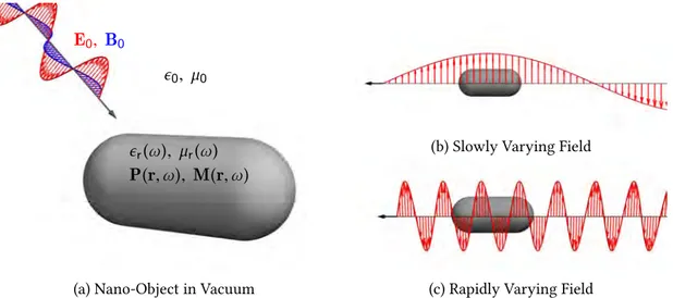
James Clark Maxwell worked out his groundbreaking equations in the s [ ], he noticed that they naturally describe a fundamental property of electromagnetic ields: he ability to propagate as waves at the speed of light – even in vacuum, independent of any carrying medium. Electromagnetic waves in a range of wavelengths from the ultraviolet to the far infrared (some 10 nm to several 10 μm) are usually referred to as light, including the visible light from around 400 nm to 700 nm. he description of efects from the interaction of light with subwavelength small particles will be the scope of this chapter.. Definition of the Problem
Generally, the goal of nano-optical problems is to ind the electric (and / or magnetic) ields in a particular nanostructure under external excitation, like illustrated in igure . a. he nanostruc-ture is usually placed in a homogeneous environment and oten lies on top of a substrate. he external excitation is usually realized by a laser beam. Other possible fundamental ields such as electron beam excitation [ ] are outside the scope of this work but can be treated formally equal to “classical” electromagnetic ields [ ].
he response of a nanoparticle to an illumination is obtained by resolving Maxwell’s equations for the given system. In the irst part of this chapter we will introduce the fundamental electro-dynamical theory. We then present a volume integral approach for the numerical resolution of Maxwell’s equations based on Green’s dyadic functions. In the last part we give an introduction to nonlinear optics and present an extension of the numerical model for the description of Second Harmonic Generation.
. Electrodynamics
. . Maxwell’s EquationsAll kind of electromagnetic phenomena are entirely explained by the four Maxwell’s equations which write (in SI units):
divD = ρ ( . a)
rotE = −∂∂tB ( . b)
divB = 0 ( . c)
rotH = ∂D
∂t + j ( . d)
with the current density j, the charge density ρ, the electric ield E and electric displacement D as well as the magnetic ield B and the magnetizing ield H. All above ields are functions of space (r) and time (t). Interaction of mater with light is described by solutions for the electromagnetic ields that fulill Maxwell’s equations for the considered system. Most commonly, the electric displacement is related to the electric ield using the electric polarization density P
D = ϵ0E + P ( . )
and the magnetizing ield to the magnetic ield using the magnetization density M H = 1
µ0
B− M ( . )
he response of material to ields is represented by this electric polarization and magnetization (see igure . a). hey are deined as the electric dipole moment dp and the magnetic moment dm per volume element dV , respectively (for details, see e.g. [ , chapter . and . ]):
P = dV =dp ϵ0χ E ( . a)
M = dmdV = χmH ( . b)
Like the ields, both the polarization and the magnetization are functions of space and time. he right-hand side terms are irst-order Taylor expansions of P and M as function of the electric and magnetizing ields, respectively. hese linear approximations are valid only for linear materials. We will see in section . , that we can describe non-linear efects by introducing higher-order terms to the equations for the polarization and magnetization.
ϵ0, µ0
E0, B0
ϵr(ω), µr(ω)
P(r, ω), M(r, ω)
(a) Nano-Object in Vacuum
(b) Slowly Varying Field
(c) Rapidly Varying Field
Figure . : (a) shows an arbitrary object placed in vacuum made of a material characterized by ϵr and µr.
Its response to incident electromagnetic ields E0, B0can be described by the polarization P
and the magnetization M. In (b) a nano-object which is small compared to the wavelength is shown, whereas in (c) a particle is shown with large size compared to the wavelength.
. . Dielectric Permitivity
he above equations together with eq. ( . ) and ( . ) yield the so called constitutive relations [ , chapter . ]
D = ϵ0ϵrE ( . a)
B = µ0µrH ( . b)
with χ = ϵr − 1 and χm = µr − 1. ϵr and µr are the relative dielectric permitivity and
mag-netic permeability, respectively. hey are deined as the ratios of the material’s permitivity and permeability relative to the vacuum values ϵ0and µ0.
For simplicity, we will consider in the following only non-magnetic media, i.e. we assume µr = 1 and consequently M = 0.
he dielectric permitivity describes the wavelength dependent response of a material to elec-tromagnetic ields. All interplaying physical efects are phenomenologically combined in this material constant. he refractive index is linked to ϵr and µr by
n =√ϵrµr =√ϵr (non-magnetic media) ( . )
Note that ϵr is complex in our notation, the imaginary part is responsible for energy dissipation.
For details see for example [ , chapter . ].
In the following, we will give a brief comparison of the dielectric behavior of metals and di-electrics.
200 300 400 500 600 700 800 900 1000 wavelength (nm) −40 −20 0 20 40 60 rel a tiv e p er mitiv ity ϵ Re(ϵr) Im(ϵr) 0 1 2 3 4 5 6 7 refr a ctiv e in d ex n (a) Gold 200 300 400 500 600 700 800 900 1000 wavelength (nm) −40 −20 0 20 40 60 rel a tiv e p er mitiv ity ϵ 0 1 2 3 4 5 6 7 refr a ctiv e in d ex n Re(n) Im(n) (b) Silicon
Figure . : Dispersion of gold (a) and silicon (b). he permitivity is drawn in red, the refractive index in black color. he respective real parts are shown with solid, imaginary parts with dashed lines.
. . . Metals
In metals, an impinging electromagnetic wave induces collective oscillations of the conduction electrons, so-called surface plasmon polaritons (SPP) [ ]. Because of electromagnetic screening due to the free carriers at visible frequencies, those oscillations are bound to a small volume at the surface of the metal, characterized by the skin-depth [ ] (see eq. ( . )). he screening efect is described by a negative real part of the dielectric permitivity, leading to purely evanescent ields inside metals. he collective electron oscillations can be driven to a resonance at the so-called plasma frequency ωp.
he permitivity of gold (from [ ]) is shown as an example in Fig. . a. he non-zero Im(ϵr)
is responsible for thermal dissipation. As consequence of this, together with the negative real part of ϵr, the imaginary part of the refractive index n is much larger than its real part. his
generally relects the fact that electromagnetic waves are strongly damped inside the metal. he relative permitivity of metals can be roughly approximated by the Drude model [ ]. Following the notation of Johnson and Christy [ ], the permitivity can be writen using a Lorentzian oscillator model
ϵr(ω) =
ωp2 ω2p− ω2
− iω/τe
( . ) with the electron relaxation time τe and the plasma frequency ωp[ , chapter ]
τe = mσ Nee2 , ωp = √ Nee2 ϵ0m ( . ) where ϵ0is the vacuum permitivity, σ the Drude conductivity, Ne the electron number density,
ethe electron charge and m its efective mass. For frequencies suiciently far below the plasmon resonance at ωp, this is a reasonable approximation.
. . . Dielectrics
In dielectrics, the absence of free charge carriers results in an entirely diferent dispersion rela-tion. Dielectrics respond to electric ields by a local displacement of bound charges relative to the latice atoms. No screening takes place and electromagnetic ields can propagate inside the medium. herefore, the relative permitivity is positive in dielectrics.
In Fig. . b, the dispersion of silicon (from [ ]) is shown as an example. If the photon energy is lower than the direct band gap (in Si at around 370 nm), the dielectric constant is mainly real and positive valued. he refractive index is also almost purely real and very high – between 3 and 4 throughout the visible and infrared. In consequence silicon absorbs very litle compared to metals. If the photon energy is higher than the direct bandgap, free carriers can be excited and the dielectric permitivity is not necessarily positive anymore. his can be seen in the silicon dispersion below λ ≈ 370 nm
Generally, the dispersion of dielectrics can also be described by an oscillator model, formally equal to equation ( . ). For silicon, very accurate dispersion models for the visible spectral range exist, using multiple oscillators [ , ].
. . uasistatic Approximation
Before we elaborate a way to obtain general solutions of Maxwell’s equations, let’s consider a particular case of light-mater interaction. In structures whose dimensions are much smaller than the wavelength, thus d ≪ λ0, efects induced by a varying ield amplitude along a structure
(so-called retardation) can usually be neglected. Such a situation is shown in igure . b. he electric ield over the whole particle is regarded as totally in phase. his is referred to as the qua-sistatic approximation, in which the displacement current ∂D/∂t is neglected and equation ( . d) simpliies to
rotH ≈ j ( . )
which is known as Ampere’s law.
For metal nanoparticles, the ield decays exponentially from the surface towards the bulk core. In this case, the quasistatic approximation requires the further condition that the size of the nanoparticle is small compared to the skin depth [ ]
dskin= λ0 2π √ ϵ0+ ϵr ϵ02 ( . ) which is given here for a particle of permitivity ϵrplaced in vacuum. For metal structures
signif-icantly smaller thandskin, the internal ield can be considered homogeneous over the nanoparticle and proportional to the external ield.
Many theoretical models in nano-optics are based on this approximation. A prominent exam-ple is the so called Rayleigh scatering, scatering from very small subwavelength particles in the quasistatic limit [ ]. Rayleigh scatering is responsible for the blue color of the sky. As we will see in more detail in section . , also second harmonic generation from dielectric nanopar-ticles can be analytically described by making simpliications like the assumption of quasistatic ields [ , ].
k
E B
Figure . : Sketch of a monochromatic electromagnetic wave.
. . Problems Including Retardation Efects
he quasistatic approximation can only be applied on particles whose size is signiicantly smaller than the wavelength of the incident light. For particles large compared to the wavelength like the one illustrated in igure . c, retardation efects occur and Maxwell’s equations must be solved rigorously in order to describe the resulting phenomena.
. . . Time Harmonic Fields in Phasor Representation
We will see that it is of enormous practical advantage to consider monochromatic ields. his is not such a restriction as it might occur in the irst place because the use of harmonic waves as ansatz for the solution of Maxwell’s equations can subsequently be generalized to arbitrarily time-dependent ields by a superposition of harmonic ields and inverse Fourier transformation. In the following, we will therefore express all ields using complex exponentials:
E(r, t ) = ˆE0(r)ei(−ωt +ϕ) ( . )
with the amplitude ˆE0, the wavevector k0, the angular frequency ω and a phase ϕ. As we treat
harmonic oscillations, the angular frequency is a convenient way to express the wavelength λ and writes:
ω = 2πc
λ = k0c ( . )
with the wavenumber k0 =|k0| and the speed of light c
c = √ϵ1
0µ0
( . ) It is possible to separate the phase ϕ from the argument of the exponential in eq. ( . ) and include it in the complex amplitude:
E(r, t ) = ˆE0(r)e−iωteiϕ = E0(r)e−iωt ( . )
he amplitude E0(r) = ˆE0(r)eiϕ is called a phasor or, more literally, a complex amplitude. he
complex plane ϕ (r) = atan ( Im(E0(r) ) ,Re(E0(r) ) ) . ( . )
ϕ is also a function of space. he real part of the complex ield E(r, t) represents the physical amplitude of the electric ield at time t. We note that it is possible to sum, substract or diferentiate phasors without limiting the generality.
he above expressions hold equally for the magnetic ield of electromagnetic waves. . . . Wave Equation
he time-harmonicity of the ields can now be used to explicitly perform the diferentiation ∂/∂t in equations ( . ) which leads to the macroscopic, Fourier transformed Maxwell’s equa-tions (compare with [ , chapter . ]):
divD(r, ω) = ρ(r,ω) ( . a)
rotE(r, ω) = iωB(r,ω) ( . b)
divB(r, ω) = 0 ( . c)
rotH(r, ω) = −iωD(r,ω) + j(r,ω) ( . d)
Maxwell’s equations represent a coupled system of linear, partial diferential equations. hey can be decoupled by applying the vectorial curl operator (rotA = ∇ × A) on equation ( . b) and substituting with eq. ( . d). By then making use of the relations between the electric ield and the displacement and between magnetizing ield and magnetization (Eqs. ( . ) and ( . )), we obtain
rot(rotE) = iω rotB
= iωµ0(rot(H + M)) = iωµ0(−iωD + j) = iωµ0(−iωϵ0ϵrE + j) = ϵr ω2 c2E + iωµ0j ( . )
We consider non-magnetic media and therefore M = 0. Using the identity
∇ × (∇ × A) = ∇(∇A) − ∆A ( . )
and
D = ϵ0E + P ⇒ divD = ϵ0divE + divP = 0 ( . )
we ind ϵr ω2 c2E + ∆E = −1 ϵ0ϵr∇(divP) − iωµ 0j. ( . )
Eq. ( . ) means that we consider only media with vanishing free charge density (ρf= 0 → ρ = ρb ), in order to be able to make some further simpliications .
ρbis the bound charge density where by deinition holds ρb=−divP, see for example [ , chapter . . ]
he reason why the simpliication of a dielectric constant works also in the case of metals where free carriers
With the speed of light c2
= (ϵ0µ0)−1and the wavenumber inside the non-magnetic medium
k =√ϵrk0 =√ϵrωc−1this becomes
(∆ + k2)E = −1
ϵ0ϵr∇∇P − iωµ
0j. ( . )
In linear materials, dipolar approximations of the bound charge density ρb(r, ω)and the current density j(r, ω) can be developed by means of the electric polarization ( . a)
ρb =−∇P ( . )
j = ∂
∂tP =−iω P. ( . )
While the later relation is evident because we are assuming time-harmonic ields, Eq. ( . ) can be easily derived from the deinition of the electric polarization density (see for example [ , chapter . . ]).
Inserting ( . ) in equation ( . ) (we included Eq. ( . ) in our derivation already using Eq. ( . )) eventually brings us to the wave equation for the electric ield:
(∆ + k2)E =−ϵ1 0ϵr∇∇P + ω 2 µ0P ( . ) (∆ + k2)E =− 1 ϵ0ϵr ( k2+∇∇ ) P. ( . )
We want to point out, that this equation is formally identical to the mechanical wave equation describing for example an oscillating string [ , chapter . ]. In the case of the electromagnetic wave equation, the speed of the propagation is the speed of light c which eq. ( . ) contains implicitly through the wavenumber k. Furthermore the waveequation is found to be a more general form of Poissons’ equation in electrostatics, which it becomes in the static case, i.e. when k = 0 [ ].
While we will limit our considerations to non-magnetic media, we point out as a inal note that an analogous wave equation can be found likewise for the magnetic ield (see for example [ , chapter . ]).
. . Green’s Functions
In order to solve an inhomogeneous linear partial diferential equation like the wave equation, the concept of Green’s functions is a versatile tool. At irst we want to illustrate the basic idea. For this we start with a diferential equation
LA(x ) = д(x ) ( . )
integrating the macroscopic system, free charge carriers only exist if the metal is actually charged. If this is not the case, a dielectric function can indeed be used to describe the metal’s optical properties including plasmonic efects.
where L is an arbitrary linear diferential operator and д(x) the inhomogeneity of the diferential equation. It would be pleasant to obtain something like an inverse of the diferential operator L in order to write A(x) = L−1д(x ). Unfortunately, the operator L can in general not be inverted .
he principle idea is therefore to search an operator G for which holds
LG = 1 ( . )
If it is possible to ind such an operator G, we obtain also a particular solution of eq. ( . ): LA(x ) = (LG)д(x ) = L(Gд(x )) ⇒ A(x ) = Gд(x ) ( . ) Instead of searching an operator G for the inhomogeneity “1” as we did in eq. ( . ) for our demonstration, it turns out to be of more general use to consider a point-source-like inhomo-geneity deined by a Dirac delta function δ (x − x′)
LG (x, x′) = δ (x− x′) ( . )
Note that in general, the Green’s function G deined by eq. ( . ) is not only dependent on the parameter of the diferential equation (here x), but also on the position of the inhomogeneity x′.
Multiplication with the original inhomogeneity and integration of eq. ( . ) leads to ∫ LG (x, x′)д(x )dx = ∫ δ (x − x′)д(x )dx = д(x ) = LA(x ) ( . )
Making use of the linearity of L we inally have: A(x ) =
∫
G (x, x′)д(x )dx ( . )
hus we solved the diferential equation for arbitrary inhomogeneities д(x), provided that G can be found from eq. ( . ). Note that we assumed here that L can be pulled out of the integral in eq. ( . ).
. . Green’s Function for the Electromagnetic Wave Equation
Let’s write again the wave equation for the electric ield (eq. ( . )) (∆ + k2)E =− 1
ϵ0ϵr
(
k2+∇∇)P ( . )
By assuming time-harmonic ields, we could eliminate the time-derivatives in Maxwell’s equa-tions which rendered eq. ( . ) to the form of a Helmholtz equation:
(∆ + k2) A(x ) = д(x ) ( . )
As depicted in section . . , the associated Green’s function G0is deined by considering a Dirac
function as inhomogeneity:
(∆ + k2) G0(x, x′) = δ (x− x′). ( . )
From this deinition, G0is found to be
G0(r, r′) = 1 4π · e± ik |r−r′| |r − r′| = e± ikR 4πR . ( . )
In the later equation, we replaced the parameter x by the distance R = |R| = |r − r′| between
source point r′and observation position r. For a detailed derivation of eq. ( . ) see for example
[ , chapter . ] or [ , chapter . ].
he scalar Green’s Function for the wave equation (equation ( . )) corresponds to an incom-ing (minus sign) or outgoincom-ing (plus sign) spherical wave. Ater equation ( . ), solutions of the wave equation can be writen as an integral over this scalar Green’s function. his is equivalent to a superposition of spherical waves and thus identical to the Huygens-Fresnel principle.
. . Dyadic Green’s Function
An electric dipole oscillating in X direction will in general induce an electric ield with x,y and zcomponents. As a consequence, the scalar Green’s function (eq ( . )) is not fully suicient to develop solutions of the wave equation. We therefore need to extend the scalar Green’s function to a notation that corresponds to the vectorial character of the ields. Following [ , chapter
. ], we can deine a Green’s function for each component of the electric ield
(∆ + k2) Gx(r, r′,ω) = nx · δ (r − r′) ( . )
where Gx is a vector composed of scalar Green’s Functions and nx is the unit vector in X
direc-tion. By doing the same for the Y and Z direction and the according components of the electric polarization, we can write
(∆ + k2) Gdyad(r, r′,ω) = I· δ (r − r′) ( . ) with the unit tensor I. Gdyad(in bold type) is a tensor with 3 × 3 components (because we are
dealing with three-dimensional ields) and is called a Green Dyad, Green tensor or Dyadic Green’s function. Dyadic Green’s functions are a tight notation for N N -dimensional Green’s functions. In the following, we will deine the Dyadic Green’s function slightly diferently. he concept however is identical to the here presented description.
. Green Dyadic Method
Ater having presented the theoretical basis of electrodynamics and a short introduction to Green’s formalism in the previous section, we now want to explicitly solve the wave equation for an arbitrary object placed in a homogeneous environment. For simplicity, we continue consid-ering monochromatic (i.e. time-harmonic) waves propagating in linear, isotropic, homogeneous and non-magnetic media.