T
T
H
H
È
È
S
S
E
E
En vue de l'obtention du
D
D
O
O
C
C
T
T
O
O
R
R
A
A
T
T
D
D
E
E
L
L
’
’
U
U
N
N
I
I
V
V
E
E
R
R
S
S
I
I
T
T
É
É
D
D
E
E
T
T
O
O
U
U
L
L
O
O
U
U
S
S
E
E
Délivré par l'Université Toulouse III - INP Toulouse
Discipline ou spécialité : Micro-ondes Electromagnétisme et Optoélectronique
JURY
M. Hervé AUBERT (Directeur de Thèse), Professeur, ENSEEIHT, LAAS, Toulouse M. Ronan SAULEAU (Rapporteur), Professeur, IETR, Rennes
Mme. Elodie RICHALOT (Rapporteur), Maître de conférences, ESYCOM, Marne-la-Vallée M. Jun-Wu TAO, Professeur, ENSEEIHT, Toulouse
M. Manos M. TENTZERIS, Professeur, ATHENA, Georgia Tech, Etats-Unis M. Fabio COCCETTI, Docteur, NovaMEMS, LAAS, Toulouse
INVITED
M. André BARKA (ONERA) M. Maxime ROMIER (CNES)
Ecole doctorale : Ecole Doctorale Génie Electrique, Electronique, Télécommunications (GEET) Unité de recherche : Laboratoire d’Analyse et d’Architecture des Systèmes (LAAS)
Directeur(s) de Thèse : M. Hervé AUBERT
Rapporteurs : M. Ronan SAULEAU, Mme. Elodie RICHALOT Présentée et soutenue par Aamir RASHID Le 21 Juillet 2010
Titre : Electromagnetic modeling of large and non-uniform planar array structures using Scale Changing Technique (SCT)
To my parents
ACKNOWLEDGEMENTS
The research work presented in this manuscript has been carri ed out at LAAS (Laboratoire d’Analyse et d’Architecture des Systèmes) as pa rt of the Research Group MINC. I would first of all like to extend my gratitude to Mr. Raja CHATILA (Director LAAS) for welcoming me to this lab and Mr. Robert PLANA (Director Group MINC) for accepting me as a member of his research group.
I am highly indebted to Hervé AUBERT, my thes is advisor, who has proposed this research topic to me and has rigorously followed and c ontributed to my research work over the last three and a half years of my thes is. I would like to thank him for his ava ilability for advice and discussion in spite of his charged schedule. He has been a constant source of inspiration through both the highs and lows of my thesis.
Special thanks go to Ronan SAULEAU (Unive rsité de Rennes 1) and Elodie RICHALOT (Université Paris-Est Marne-la-Vallée) for accepting to review my thesis as ‘rapporteurs’ on a very short notice. I highly appr eciate their in-depth review of this manuscript and their detailed comments and remarks that greatly helped me to improve the quality of this
manuscript.
I am equally grateful to Jun-Wu TAO (INP-T oulouse), Manos TENTZERIS (Georgia Tech) , Fabio COCCETTI (NovaMEMS), André BARKA (ONERA) and Maxime ROMIER (CNES) for accepting to be the part of the evaluation committee of my thesis defense. I highly appreciate their keen interest in my work as well as their precious comments and questions during the course of my defense.
I cannot forget the help and encouragement I got from Nathalie RAVEU (ENSEEI HT-INP
Toulouse) during the first year of m y thesis. I thank her for helping me in understanding the theoretical concepts of Scale Changing Technique as well as the MATLAB codes.
I would also like to thank my colleagues Euloge TCHIKAYA, Fadi KHALIL, and Farooq
Ahmad TAHIR for the help, di scussions and collaboration regar ding my research work. I would also like to acknowledge the help of Ahmad ALI MOHAMED ALI (regarding IE3D), Alexandru TAKACS (r egarding F EKO), Ga etan PRIGENT (regarding HFSS) and Sami HEBIB throughout the course of my thesis.
I would also like to extend my thanks to Hervé LEGAY (THALES) who has helped and
4
I am equally indebted to Brigitte DUCROCQ (secretary Group MINC) for her help in dealing with all the administrative stuff that allowed me to concentrate on my work.
I will a lways be grateful for the support and encouragement that I received from my
colleagues of Group MINC. I am thankful to all of them for providing a healthy and friendly work environment. My special thanks go to my office mates (Mai, Euloge, Farooq, Sami and Dina) for a great company and support.
I am extremely grateful to my parents for their encouragement, patience, support and prayers throughout my thesis and to my younger sister Aasia for her funny anecdotes and family updates that kept my spirits high during the stressful times.
I am very thankful to a number of my friends who have made my stay in Toulouse joyous and exhilarating. I would like to extend my thanks to Rameez Khalid and Asif Inam who helped me to settle when I was new in the city. I cannot thank enough my friend Naveed who has always been there ready to help and w hose delicious m eals I will alwa ys miss. I woul d also like to thank my friends A li Nizam ani, Usman Zabit, Ahmad Hayat, Mohamed Cheikh, Assia Belbachir, Lavindra de silva for such a great time.
Last but not the least I would like to acknowledge the financial support by Thales Alenia Space and Regional council of Midi-pyrennes wit hout which this research work would not have been possible.
5
TABLE OF CONTENTS
ABSTRACT
GENERAL INTRODUCTION
SECTION I: THEORY OF SCALECHANGING TECHNIQUE
I.1. INTRODUCTION ... 16
I.2. SCALE-CHANGING TECHNIQUE (SCT) ... 18
I.2.1. Introduction ... 18
I.2.2. Discontinuity Plane ... 18
I.2.2.1. Partitioning of the Discontinuity Plane ... 19
I.2.2.2. Choice of Boundary Conditions: ... 21
I.2.2.3. Field Expansion on the Orthogonal Modes: ... 22
I.2.2.4. Active and Passive Modes: ... 22
I.2.3. Scale-changing Network (SCN) ... 23
I.2.4. Scale-changing Sources ... 26
I.3. MODELING OF A PASSIVE PLANAR REFLECTOR CELL USING SCALE-CHANGING TECHNIQUE (SCT) ... 30
I.3.1. Introduction ... 30
I.3.2. Geometry of the Problem ... 30
I.3.3. Application of Scale-changing Technique ... 31
I.3.3.1. Partitioning of Discontinuity Plane: ... 31
I.3.3.2. Surface Impedance Multipole Computation: ... 32
I.3.3.3. Scale-changing Network Computation: ... 37
I.3.3.4. Network Cascade: ... 40
I.3.4. Results Discussion ... 41
I.3.4.1. Planar Reflector under Normal Incidence: ... 41
I.3.4.2. Planar Reflector under Oblique Incidence: ... 45
I.4. CONCLUSIONS ... 50
6
SECTION II: ELECTROMAGNETIC MODELING USING SCALECHANGING
TECHNIQUE (SCT)
II.1. INTRODUCTION ... 52
II.2. MODELING OF INTER-CELLULAR COUPLING ... 54
II.2.1. Bifurcation Scale-changing Network ... 54
II.2.1.1. Equivalent Circuit Diagram: ... 55
II.2.2. Mutual Coupling between half-wave dipoles ... 60
II.2.2.1 Simulation Results ... 62
II.3. MODELING OF NON-UNIFORM LINEAR ARRAYS (1-D) ... 65
II.3.1. Introduction ... 65
II.3.2. Characterization of a metallic-strip array ... 65
II.3.2.1 Application of Scale-changing Technique ... 66
II.3.2.2 Simulation Results and Discussion ... 70
II.3.3. Characterization of a metallic-patch array ... 75
II.3.3.1 Introduction ... 75
II.3.3.2 Simulation Results and Discussion ... 76
II.4. MODELING OF 2-D PLANAR STRUCTURES ... 79
II.4.1. Introduction ... 79
II.4.2. Mutual coupling with 2-D Scale-changing Network ... 79
II.4.3. Formulation of the scattering problem ... 82
II.4.3.1 Derivation of the current density on the array domain D ... 82
II.4.4. Numerical results and discussion ... 89
II.4.4.1 Planar Structures under Plane-wave incidence ... 90
II.4.4.2 Planar Structures under Horn antenna ... 95
II.4.4.3 SCT Execution Times ... 104
II.5. CONCLUSIONS ... 106
CONCLUSIONS
APPENDIX A
A.1. INTRODUCTION ... 112A.2. ELECTRIC BOUNDARY CONDITIONS ... 112
A.3. MAGNETIC BOUNDARY CONDITIONS ... 112
A.4. PARALLEL-PLATE WG BOUNDARY CONDITIONS ... 113
7
APPENDIX B
B.1. INTRODUCTION ... 115
B.2. APPROXIMATION BY RADIATING APERTURE ... 115
B.3. TANGENTIAL COMPONENT OF FAR-FIELD ON A PLANAR SURFACE ... 116
B.3.1. Horn centered on the planar surface ... 116
B.3.1. Horn with an offset and an inclination angle ... 117
B.4. CALCULATION OF ... 119
B.4.1. Horn centered ... 119
B.4.2. Horn at an offset with an inclination ... 120
THESIS SUMMARY (FRENCH)
REFERENCES
PUBLICATIONS
9
Large sized planar structures are increasingly being employed in satellite and radar applications. Two major kinds of such structures i.e. FSS and Reflectarrays are particularly the hottest domains of RF design. But due to their large electrical size and complex cellular patterns, full-wave analysis of these structures require enormous amount of memory and processing requirements. Therefore conventional techniques based on linear meshing either fail to simulate such structures or require resources not available to a common antenna designer. An indigenous technique called Scale-changing Technique addresses this problem by partitioning the cellular array geometry in numerous nested domains defined at different scale-levels in the array plane. Multi-modal networks, called Scale-changing Networks (SCN), are then computed to model the electromagnetic interaction between any two successive partitions by Method of Moments based integral equation technique. The cascade of these networks allows the computation of the equivalent surface impedance matrix of the complete array which in turn can be utilized to compute far-field scattering patterns. Since the computation of scale-changing networks is mutually independent, execution times can be reduced significantly by using multiple processing units. Moreover any single change in the cellular geometry would require the recalculation of only two SCNs and not the entire structure. This feature makes the SCT a very powerful design and optimization tool. Full-wave analysis of both uniform and non-uniform planar structures has successfully been performed under horn antenna excitation in reasonable amount of time employing normal PC resources.
11
The accurate prediction of the plane wave scattering by finite size arrays is of great practical interest in the design and optimization of modern frequency selective surfaces, reflectarrays and transmittarrays. A complete full-wave analysis of these structures demands enormous computational resources due to their large electrical dimensions which would require prohibitively large number of unknowns to be resolved. Thus the unavailability of efficient and accurate design tools for these applications limits the engineers with the choice of low performance simplistic designs that do not require enormous amount of memory and processing resources.
Moreover the characterization of large array structures would normally require a second step for optimization and fine-tuning of several design parameters since the initial design procedure assumes several approximations e.g. in the case of reflectarrays the design is usually based on a single cell scattering parameters under normal incidence, which is not the case practically. Therefore a full-wave analysis of the initial design of the complete structure is necessary prior to fabrication, to ensure that the performance conforms to the design requirements. A modular analysis technique which is capable of incorporating small changes at individual cell-level without the need to rerun the entire simulation is extremely desirable at this stage.
12
Historically several approaches have been followed when analyzing large planar structures [Huang07]. In the case of uniform arrays, where we have periodicity in the geometry, an infinite approach is often used. By using Floquet’s theorem, the analysis is effectively reduced to solving for a single unit-cell; thus significantly reducing the unknowns and therefore the simulation times [Pozar84] [Pozar89]. Although the periodic boundary conditions take into account the effect of mutual coupling in the periodic environment, the approximation may not hold for the arrays where individual cell geometries are very different. In addition this is a very poor approximation for the cells lying at the edges of the array.
A simple method based on Finite Difference Time Domain (FDTD) technique has been proposed to precisely account for the mutual coupling effects. It consists of illuminating a single cell in the array in the presence of nearest neighbor cells and calculating the reflected wave. Though it allows precise excitation and boundary conditions for each cell in the array it is not very practical to design large arrays due to extremely long execution times [Cadoret2005a].
Different conventional methods have been tested for a full-wave analysis of periodic structures e.g. Method of Moments (MOM) used in the spectral domain for multilayered structures [Mittra88] [Wan95], Finite Element Method (FEM) [Bardi02] and FDTD [Harms94]. But all of these methods would require prohibitive resources for the cases where the local periodicity assumption cannot be applied. A spectral domain immitance approach has been used in the full-wave analysis of a 2-D planar dipole array along with the Galerkin’s procedure using entire domain basis functions [Pilz97].
The method of moments for the global electromagnetic simulation of finite size arrays requires high CPU time and memory especially when the patch geometries are non-canonical and therefore sub-domain basis functions have to be used. The memory problem may be resolved by using various iterative techniques (e.g. Conjugate Gradient iterative approach) [Sarkar82] [Sarkar84] at the cost of further increase in the execution time. A promising improvement of the MOM, called the
13
time and memory storage for large-scale structures [Mittra05] [Lucente06]. However the convergence of numerical results remains delicate to reach systematically.
In order to overcome the above-mentioned theoretical and practical difficulties, an original monolithic formulation for the electromagnetic modeling of multi-scale planar structures has been proposed [Aubert09]. The power of this technique called the Scale-changing Technique (SCT) comes from the modular nature of its problem formulation. Instead of modeling the whole planar-surface as a single large discontinuity problem, it is split into a set of many small discontinuity problems each of which can be solved independently using mode-matching variational methods [Tao91]. Each of the sub-domain discontinuity solution can be expressed in the matrix form characterizing a multiport-network called Scale-Changing Network (SCN). SCT models the whole structure by interconnecting all scale-changing networks, where each network models the electromagnetic coupling between adjacent scale levels.
The cascade of Scale Changing Networks allows the global electromagnetic simulation of all sorts of multi-scaled planar geometries. The global electromagnetic simulation of structures via the cascade of scale-changing networks has been applied with success to the design and electromagnetic simulation of specific planar structures such as multi-frequency selective surfaces of infinite extent [Voyer06], discrete self-similar (pre-fractal) scatterers [Voyer04] [Voyer05], patch antennas [Perret04] [Perret05] and reconfigurable phase-shifters [Perret06] [Perret06a]. The objective of this work is to validate SCT in the case of various planar array geometries including FSS arrays, reflectarrays and transmittarrays.
Another modular approach based on spectral-domain MOM has been used in the case of multilayer periodic structures [Wan95] which consists of characterizing each array layer by a generalized scattering matrix (GSM) and then analyzing the complete structure by a simple cascade of these GSMs. SCT differs from this approach because in case of SCT partitioning is applied to the same array-plane and therefore SCT is applicable for the single-layer array problems. For multilayer arrays SCT can be used in hybrid with the fore-mentioned approach for the efficient modeling of more complex electromagnetic problems e.g. in the case of variable
14
sized stacked patch-arrays [Encinar99] [Encinar01] [Encinar03] and aperture-coupled arrays [Robinson99] [Keller00].
This thesis is divided into two main sections. In the first section the theory behind the scale-changing technique is presented in a general context using an example of a generic discontinuity plane. Several concepts related to the technique are introduced and elaborated. How the discontinuity problem can be expressed in terms of equivalent circuit components is demonstrated [Aubert03]. The problem is then formulated in terms of matrix equations from this equivalent circuit and solved using MOM based technique. The second part of this section demonstrates the application of SCT to periodic reflectarrays.
In the second section of the thesis, SCT is used to model finite and non-uniform single layered planar arrays. First it is shown that SCT effectively models the electromagnetic coupling between the neighboring cells of an array. Later the technique is used to model linear arrays of non-uniform metallic strips and patches. The simulation results as well as the simulation times are compared to the classic simulation tools. Finally, SCT is applied to find the free-space diffraction patterns of two-dimension planar arrays. Both uniform and non-uniform arrays are simulated under plane-wave and horn-antenna excitations and the scattering field plots are compared to results obtained by other techniques.
SECTION I:
THEORY OF SCALE-CHANGING
TECHNIQUE
16
I.1. INTRODUCTION
Presently the most common method to compute the scattering fields from the planar structures is by solving the integral equation formulation of the Maxwell’s equations. This approach permits to express the open boundary electromagnetic problem in terms of an integral equation formulated over the finite planar surface. This reduction of one spatial dimension makes this method very efficient in the case of planar geometries. Yet this method in its traditional formulation is not particularly adapted for large planar structures containing scaled geometries and complex metallic patterns. Rapid and fine-scale variations in the structure geometry can cause abrupt changes in electromagnetic field patterns requiring local meshing at a very minute scale which in turn would require immense storage and computational resources.
We propose to resolve this problem by introducing local description of fields for different regions of the planar surface. The procedure can be outlined in the following steps:
1) The planar surface is decomposed in several sub-domain surface regions. 2) The electromagnetic fields are expressed on the modal-basis of each of these
17
3) Modal contributions are treated separately for lower order modes and higher order modes. Higher order modes are considered to contribute only locally where as lower order modes define coupling with the domain at the higher scales.
4) Electromagnetic coupling between two successive scales is modeled by a scale-changing network defined by the lower order modes of the two sub-domains.
5) A global electromagnetic solution is obtained by a simple cascade of these scale-changing networks.
18
I.2. SCALE-CHANGING TECHNIQUE (SCT)
I.2.1. Introduction
Electrically large (many orders of the wavelength) structures e.g. multiband frequency selective surfaces, non-uniform reflectarrays and self-similar fractal structures are said to be complex when their geometrical dimensions vary over a large range of scale. In other words we have very fine patterns and large patterns in the same structure. As mentioned previously linear meshing in these structures requires tremendous amount of computational resources and may lead to ill-conditioned matrices.
The higher the number of scale-levels the higher is the complexity. Scale-changing technique (SCT) gets its name from scaled partitioning of the planar structure and the modeling of the electromagnetic interactions between these scale-levels [Aubert09]. In this section we will focus on the electromagnetic simulation of a generic multi-scale structure consisting of metallic patterns printed on a dielectric planar surface.
I.2.2. Discontinuity Plane
To understand the concepts and workings of the Scale-changing Technique we will study a general case of an arbitrary discontinuity. Consider multiple metallic patterns with the dimension varying over a wide range of scale, printed on a planar dielectric surface. Suppose that the largest patterns are several orders of magnitude bigger than the finest patterns. This discontinuity plane may be modeled by placing it at a cross-section of a waveguide or can simply be located in the free-space. The two half-regions i.e. the left-hand region and the right hand region are assumed to be composed of multilayered and loss-less dielectric media.
19
I.2.2.1. Partitioning of the Discontinuity Plane
The starting point of proposed approach involves the coarse partitioning of the discontinuity plane domain into large sub-domains of arbitrary shape and comparable sizes. This partitioning step corresponds to the first order of the magnitude of discontinuity plane patterns. The second step consists of partitioning each of the domains formed in the first step by introducing smaller sub-domains of comparable sizes corresponding to the next order of magnitude. This procedure of partitioning the domains into smaller sub-domains is repeated until the smallest scale is reached. Such hierarchical domain-decomposition allows rapid focusing on increasing details of the planar geometry unlike a linear meshing approach.
Figure I.1: An example of discontinuity plane presenting 3 scale-levels (black is metal and white is dielectric) and the scattered view of the various sub-domains generated by the partitioning process
This manner of partitioning allows us to define separate scale-levels for the co-planar domains and sub-domains and this can be represented as shown in
20
Figure- I.1. The smallest sub-domains are assigned the bottom most scale or scale-level one whereas the largest domain i.e. the entire discontinuity plane gets the highest scale-level . It is important to note that the scattered representation of the domains is only for the sake of clarity, essentially all the domains and sub-domains lie in the same plane.
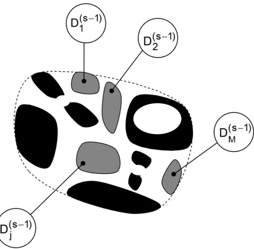
Figure I.2: The ith generic domain resulting from the partition process at scale level ‘s’ (black is metal, white is dielectric and grey indicates the location of sub-domains
(with j = 1, 2, … , M)
Let’s consider once again the case of the generic discontinuity plane of Figure-I.2. Assuming it to be the th domain of a general scale-level it can be denoted for convenience as D . where, i 1 , being the total number of domains at the scale-level . And ranging from 1 to . Using the above described partitioning procedure it can be decomposed into sub-domains denoted
21
by D , (where j 1 ) defined at scale-level . In addition the discontinuity plane may contain simple metallic and dielectric domains where further partitioning is not needed [Aubert09].
I.2.2.2. Choice of Boundary Conditions:
Artificial boundary conditions are introduced along the contours of all these domains and sub-domains. These boundary conditions are introduced only on the contours of the sub-domains lying in the discontinuity plane and not in the two half-regions on each side of this discontinuity. The boundary conditions are selected from
1) Perfect Electric Boundary Conditions (PEC) 2) Perfect Magnetic Boundary Conditions (PMC) 3) A combination of the above two conditions 4) Periodic Boundary Conditions (PBC)
The physics of the problem should be considered in the choice of the boundary conditions around any domain. In practice boundary conditions can be tried on the contours of each sub-domain and tested for accuracy, execution time and numerical convergence depending on a particular geometry.
The purpose of introducing the boundary conditions at the sub-domain level is essentially to define a new boundary value problem at a local level that can be solved independently by expressing the tangential fields in the region on the modal-basis respecting these boundary conditions. At sub-domain level each boundary value electromagnetic problem is resolved by writing the field equations in integral equation formulation and applying the Galerkin’s method to solve for the surface fields and currents.
Since now we have many smaller independent problems, the number of unknowns in the matrix equations are reduced and therefore much less memory resources are required. It is to be noted here that due to introduction of artificial boundary condition the scale-changing technique is not an exact technique but an
22
approximate method. And these approximations need to be chosen carefully not to significantly perturb the accuracy of the solution [VoyerTh].
I.2.2.3. Field Expansion on Orthogonal Modes:
In the sub-domain D bounded by the artificial boundary conditions the modal expansion of the tangential electromagnetic field can be performed. Therefore the
th mode of the modal basis , is solution to the following Helmholtz equation [Collin91].
,
,
0
(I.1)In the above equation is the transverse Laplacian operator and , is the cut-off wave-number of the nth mode of the ith sub-domain of the sth scale-level i.e. D . The , is the orthogonal modal-basis which satisfies the boundary conditions
at the contours of the sub-domain. The condition of orthognality dictates;
,
,
, ,.
,0
(I.2)
The operator represents the complex conjugate. And m and n are any two modal indexes of the orthogonal modal basis , .
I.2.2.4. Active and Passive Modes:
Now that we have the modal representation of the tangential electromagnetic field in the sub-domain, the field contributions due to lower-order and higher-order modes can be treated separately. As the order of the modes increases, the energy diffracted at the metal interface for that harmonic becomes more and more localized within the vicinity [Collin91]. Therefore it is safe to assume that after a certain number
23
of modes, the higher order modes will contribute only to very fine-scale variations of the electromagnetic field that are localized to that particular sub-domain. On the other hand the lower order modes describe the large-scale variations of the field that couples with the tangential fields of the sister sub-domains.
For example in case of the generic sub-domain D the fine-scale variations are described as a linear combination of infinite number of higher-order modes of
,
which are spatially localized in the vicinity of discontinuities, sharp edges and various contours of the domain and therefore does not significantly contribute to the electromagnetic coupling between the various sub-domains D . For this reason these higher-order modes are called passive modes.
The large-scale contribution to the field in D is due to the electromagnetic coupling between the constitutive sub-domains D . This coupling can be modeled as the combination of only a limited number of lower-order modes in the spectral domain. Because these lower-order modes are involved in the description of electromagnetic coupling they are called active modes. Finally, the coupling between the active modes of the domain D and the passive modes of sub-domains D is very weak due to the large difference in their spatial frequencies.
It follows from the above-mentioned physical considerations that the electromagnetic coupling between two subsequent scale-levels, e.g. the scale-level and the lower scale , can be defined in term of the mutual interactions of the active modes of the domain D and the active modes of the sub-domains D .
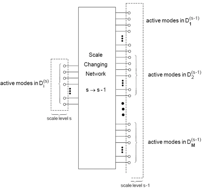
I.2.3. Scale-changing Network (SCN)
The mutual coupling of the active modes described in the previous section can be represented by a multiport of Figure I.3. Each port in the network represents an active mode. The ports on the left hand side models the active modes in domain D whereas the M set of ports on the right hand side denote the active modes of M
sub-24
domains D (where j 1 ) of scale level . As this multiport allows to relate the fields at scale s to fields at the lower scale s-1, it is named the
Scale-changing network (SCN).
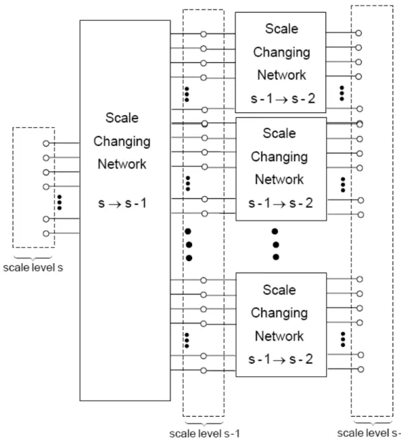
For relating the electromagnetic fields at scale to that of another scale , the interconnection of scale-changing networks may be performed as shown in Figure I.4, each network being previously computed separately. Consequently, the modeling of interaction among the multiple scales of a complex discontinuity plane is reduced to simple cascade of appropriate scale-changing networks, where each network models the interaction between two scales.
Figure I.3: The Scale Changing Network coupling the active modes in the domain (scale level s) and its constitutive sub-domains (scale level s–1)
25
It is important to note that the computation of these scale-changing networks is mutually independent. Therefore each network can be computed by using a separate processing node. This modular nature of scale-changing technique can be exploited in multiprocessing environments to cut simulation times in the case of very large and complex structures. Moreover any single change at any scale-level will only need the re-computation of two scale-changing networks and not the SCNs for all other scales. This means that small geometric changes will not require the entire simulation of the structure all over again. This feature is an essential quality of a good parametric tool. Therefore SCT designs will have the capability of rapid simulations in the cases where the effects of certain modifications are studied on the design.
Figure I.4: The cascade of Scale Changing Networks allow to relate the transverse electromagnetic field at scale ‘s’ to that at scale ‘s–2’
26
The derivation of scale-changing network’s characterization matrix requires the definition of artificial electromagnetic sources named the scale-changing sources in various sub-domains obtained from the partitioning process.
I.2.4. Scale-changing Sources
The derivation of scale-changing network that couples the scale to the adjacent scale requires the resolution of a boundary value problem. Active modes of the domain at scale-level will act as the excitation sources called scale
changing sources for the problem.
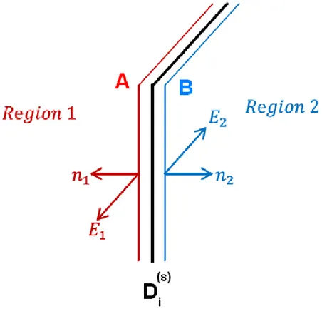
Figure I.5: The discontinuity plane along with the two parallel side-planes A and B in the two half-regions
To derive the mathematical expressions for scale changing sources lets consider once again the generic discontinuity plane D . Figure I.5 represents the discontinuity plane along with two planes A and B placed infinitely close to the either side of the discontinuity plane. The unit-vectors and are the normal vectors of
27
the two planes. The tangential electric and magnetic fields ( , and , ) on the
domains of the two parallel planes (α 1,2) can be expressed on a modal-basis
, . , ∑ , , , (I.3) , , ∑ , , , (I.4) , ,
and , , denote respectively, the voltage and current amplitudes of the
nth mode in D . Tangential electric field and the surface current density on each of
the domain can be expressed separately with active and passive modes defining the large scale and fine scale variation of these quantities respectively.
, ∑ , , , ∑ , , ,
, , , (I.5)
where is the number of active modes in each of the domain. Similarly for surface current density we can write.
, ∑ , , , ∑ , , ,
, , , (I.6)
The passive modes being highly evanescent are shunted by their purely reactive modal admittances ( , , ). Consequently,
, , , , , , for (I.7)
Using the above formulation in Equation I.6 we obtain;
, , ∑ , , , , ,
(I.8)
28
, , , ,
(I.9)
with , ∑ , , , , where , is an admittance operator.
Now the tangential electric field and surface current density on the discontinuity plane D can be determined from using the following boundary conditions.
, ,
, , (I.10)
Using the above equations we can solve for the field quantities on the discontinuity plane as follows:
∑ , , ∑ , , , ∑ , , , (I.11)
, , , , ,
Similarly can be written as
(I.12) where ∑ , , ∑ , , , ∑ , , , , , ∑ ∑ , , , , , (I.13)
If the same number of active modes are taken in the domains A and B i.e.
, the current scale changing sources at scale-level s and domain D can be rewritten in the simplified form as under:
∑ , ,
29
where , , , , , is the amplitude of the nth active mode in D and
, , , , , is the total modal admittance viewed by D in case of
passive modes. Equation I.12 can be represented as a Norton equivalent Network shown in Figure I.6.
Figure I.6: Symbolic representation of current scale-changing source at scale level ‘s’ in the domain
In the computation of a scale changing network between a domain D at scale
s and the sub-domains D at scale s-1, the scale-changing sources of the sub-domains are defined on the active modes of the respective sub-domain only. This is due to the assumption that we made in the earlier section that active modes of the larger domain interacts very weakly to the passive modes of its constituent sub-domains.
30
I.3. MODELING OF A PASSIVE PLANAR REFLECTOR CELL USING
SCALE-CHANGING TECHNIQUE (SCT)
I.3.1. Introduction
In the previous sections we have developed the basic concepts needed to understand the scale changing technique. Now we will apply these concepts to a practical case of passive planar reflector cell.
Figure I.7: A 2-D infinite reflect-array with enlarged unit-cell: Dimensions: a0=b0=15mm, a1=12mm, b2=1mm, b1 and a2 are variable. Substrate thickness h'=0.1mm (εr=3.38), air gap height h=4mm.
I.3.2. Geometry of the Problem
Consider an infinite array of Figure I.7 under plane wave excitation. This problem is equivalent to resolving the same problem for a single unit-cell under periodic boundary conditions. The computation of phase-shift introduced to an incident plane-wave by unit-cell reflectors when bounded by periodic boundary conditions is an essential step of a reflectarray design process. Characterization of each unit-cell under infinite array environment is considered as an approximation of
31
the behavior of that cell in the real array. Therefore we will consider here the problem of finding the scattering matrix of a planar reflector under infinite array conditions.
I.3.3. Application of Scale-changing Technique
I.3.3.1. Partitioning of Discontinuity Plane:
Application of scale-changing technique requires the partitioning of the discontinuity plane. In our case simplicity of the geometry allows us to define three nested scales (Figure I.8). In this simple case we have only one domain at each scale-level. Domain D of scale-level 3 encompasses the entire reflector plane. Domain D at second scale-level consists of patch and slot whereas the domain D on the bottom scale is comprised of slot only.
Figure I.8: Partitioning the discontinuity plane of the planar reflector in its constituent domains and sub-domains at three scales. White portions represent dielectric, Black represents metal and grey parts represent un-partitioned sub-domains.
This problem requires the computation of one scale-changing network i.e. between the scale-level 3 and scale-level 2 modeling the interaction between the
32
active modes of D and D . This SCN will be cascaded with a surface impedance multipole computed on the active modes of D as shown in Figure I.9.
Figure I.9: Global simulation of the planar reflector involves the cascade of the scale-changing network multipole and the surface impedance multipole.
The two multipoles can be computed separately by decomposing the original problem in two separate problems each modeling two successive scale-levels as shown in the Figure I.10. The resolution of the structure in Figure I.10 (a) will give the scale changing network multipole while the surface impedance multipole can be obtained from the structure of Figure I.10 (b).
I.3.3.2. Surface Impedance Multipole Computation:
The surface impedance multipole is represented in Figure I.10 (b). The ports on the LHS represent the active modes in domain D of scale-level 2. The boundary value problem in this case is shown in the same figure above the surface impedance multipole. Here we have the slot domain D nested inside the patch domain D , both resting on a dielectric slab of relative permittivity εr. This boundary value problem can be represented in terms of the equivalent circuit of Figure I.11.
33
(a) (b)
Figure I.10: Decomposition of the problem in two sub-problems. (a) SCN is computed from the structure shown above the SCN multipole (b) Surface Impedance Multipole is computed from the problem involving patch and slot domain only.
The left part of the circuit i.e. the source J along with the admittance operator is the Norton equivalent excitation defined on the discrete orthogonal modal-basis of D ( , ). ∑ , , , ∑ , , (I.15) ∑ , , , , (I.16) , is the number of active modes of the domain D . , and , are the
34 , , , , , , , , (I.17) ,
is the admittance of nth mode. The expressions for the modal admittances for TE and TM modes are as follows:
(I.18)
with the propagation constant of nth mode in medium . The expression of for
a TE or TM mode is
Figure I.11: Equivalent circuit diagram to compute the surface impedance multipole.
The dielectric side of the discontinuity plane is modeled as a shorted dielectric waveguide. Therefore the operator represents the modes of the domain D short circuited by ground through the dielectric. If is the thickness of the dielectric and the propagation constant of th mode in the substrate then the admittance operator can be written as
35
The electric field source E is a virtual source defined in the slot domain D (scale 1). The name virtual sources imply that unlike real sources they deliver no electromagnetic energy and are therefore represented with an arrow across the source. The virtual sources serve to represent two different boundary conditions at a time in one equivalent circuit. For example in this case the field source E defined in D models dielectric boundary conditions where as the dual quantity J which is only defined outside D models the perfect electric boundary conditions of the metallic surface.
It is to be noted here that both the quantities E and J cannot be non-zero at the same time and therefore the energy supplied by the source which is the product of the two quantities and is zero everywhere [Aubert03]. E serves to
represent the tangential electric field in the slot domain on an orthogonal set of entire domain trial functions [Nadarassin95] defined in D ( , ) as under.
∑ , , ,
D (I.20)
, being the number of active modes in D . The column-vector , of
dimensions , lists the weights of the test functions.
,
,
,
, (I.21)
Following matrix equations can be written from the equivalent circuit by using Kirchoff’s laws. E J 0 1 1 J E (I.22)
36
This boundary value problem may be solved by applying the Galerkin’s method. The above matrix equation can therefore be written in terms of coefficient matrices.
, 0 0 , , (I.23)
denotes the complex conjugate transpose of a matrix. is the projection matrix of dimensions , , of active modes of modal-basis , on , .
, , , , , , , , , , , , , , , , (I.24)
Similarly is the projection matrix of dimensions , , , of passive modes of modal-basis , on , .
, , , , , , , , , , , , , , , , , , (I.25)
is a diagonal matrix of passive modal admittances. Its dimensions are ,
, , ,
,
, 0
0 ,
, (I.26)
is a diagonal matrix of dimensions , ,
, coth 0
0 ,
, coth (I.27)
37
, (I.28)
with
,
, , (I.29)
I.3.3.3. Scale-changing Network Computation:
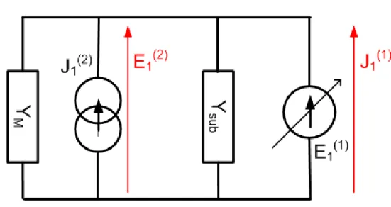
Equivalent circuit of Figure I.12 (a) represents the boundary value problem of Fig I.10 (a). In this case the discontinuity plane represented by the middle branch is modeled with two sources. The current source j is the virtual source defined in D defining perfect electric boundary conditions while the electric field source e is the
scale-changing source modeling the electromagnetic coupling with the sub-domain as explained in section I. Assuming that both sources are defined by the same set of orthogonal modes the equivalent circuit can be simplified to that of Figure I.12 (b) [PerretTh].
Z
sub 1(3) 1 (3) M e(2) (2) (2) (a)38
(b)
Figure I.12: (a) Equivalent circuit diagram to compute the scale-changing network multipole. (b) Simplified Equivalent Circuit.
is the excitation source defined on , active modes of the orthogonal modal-basis of D , . Floquet modal basis is chosen at this scale to model the periodicity of the infinite array. Floquet modes TE00 and TM00 are chosen to represent the two plane-wave polarizations. The expressions for the Floquet modal basis can be found in Appendix A.
∑ , , ,
∑ , ,
(I.30)
, and , are the column vectors of dimensions , .
, , , , , , , , (I.31)
Operators and are defined as usual
∑ , , ,
,
39 with modal impedances defined as
(I.33)
Using Kirchoff’s circuit laws following matrix equation can be written from the equivalent circuit of Fig (b)
J E E J (I.34)
Applying Galerkin’s method we get
,
, 1121 1222
,
, (I.35)
With projection matrices defined as under:
is a diagonal matrix of dimensions , ,
, tanh 0
0 ,
, tanh ,
(I.36)
is a unitary matrix of dimensions , ,
1 0
0 1
(I.37)
with and
is the projection matrix of dimensions , , , of passive modes
40 , , , , , , , , , , , , , , , , , , (I.38)
and Z is a diagonal matrix of size , , , ,
, , , , , , , , , , 0 0 , , , , , , , , , , (I.39)
I.3.3.4. Network Cascade:
In this step cascade of two networks is performed to obtain the equivalent surface impedance of the complete structure as viewed by the excitation modes
at the surface of the discontinuity plane (see Figure I.9)
,
, 1121 1222
,
, (I.40)
Note the negative sign in the surface impedance multipole equation to signify the reversal of the currents in the cascading procedure.
,
, , (I.41)
From the above equations following equation for the overall multipole can be extracted
,
, (I.42)
with
, (I.43)
Scattering parameter matrix is calculated by using
(I.44)
41
I.3.4. Results Discussion
I.3.4.1. Planar Reflector under Normal Incidence:
A planar unit-cell reflector depicted in Figure I.13 has been modeled and simulated using the approach outlined in the previous section. The discontinuity plane of the reflector cell is comprised of slotted patch centered on two dielectric layers. The dimensions are indicated in the figure captions. The simulations have been performed for nine distinct unit-cell geometries obtained by varying metallic patch width (b1) and slot length (a2) (Table-I.1). This infinitely thin metal patch rests on a 100µm lossless dielectric ( 3.38) which is in turn placed on a 4mm air-cavity with a ground-plane at the bottom. Normal plane wave with electric field linearly polarized perpendicular to slot-length is considered as excitation source. The results presented are for the phase of the reflection coefficient (S11) calculated at the plane of the discontinuity plane.
Figure I.13: Geometry of Planar unit-cell reflector. Dimensions: a0=b0=15mm, a1=12mm, b2=1mm, b1 and a2 are variable. Substrate thickness h1=0.1mm (εr=3.38), air gap height
42 I.3.4.1.1. Convergence Study:
As described in the previous section, the tangential electromagnetic field in different regions of the discontinuity plane is defined by the orthogonal set of modes of the domain. Precise description of field quantities would require adequate number of active and passive modes to be considered at each scale-level. Appropriate number of modes may be chosen by a systematic convergence study. This study involves plotting reflection coefficient phase results with respect to the number of modes at each domain to find the appropriate number for which the results converge.
Case 1 2 3 4 5 6 7 8 9
b1 2 4 4 6 6 8 10 10 12
a2 7 4 6 4 10 8 6 10 10
Table I.1: Above nine planar unit-cell geometric configurations are simulated. Dimension b1 and a2 (in mm) are the width of the patch and the length of the slot respectively.
Convergence study results for the sixth reflector-cell configuration at the centre frequency of 12.1GHz are shown in Figure I.14. Figure I.14 (a) shows the convergence of the reflection coefficient phase with respect to the number of active modes , in the patch domain D and the number of passive modes , taken inside the periodic waveguide (discontinuity domain D . It is apparent that there is no significant variation in phase results for waveguide modes greater than 2500. Similarly around 600 active modes in the patch domain are required for the phase convergence with in 3º margin.
Figure I.14 (b) plots the convergence curves with respect to patch active modes and the number of active modes , taken in the slot domain D . Here, again the flat part of the curves demonstrates the convergence of reflected phase. It is evident from the curves that convergence is achieved if the number of patch active modes is taken between 600 and 1000 and the number of slot active modes is taken between 80 and 120. However, if the number of slot active modes exceeds a certain limit, matrices become ill-conditioned leading to the loss of convergence as can be seen by the sudden drop in two lower curves. This numerical problem can be
43
attributed to the use of entire domain trial functions and is analogous to the one observed classically in the Mode Matching Technique [Lee71].
(a)
(b)
Figure I.14: Convergence study of phase of reflection coefficient for case6 (b1,a2)=>(8,8), Frequency 12.1GHz : (a) Convergence with respect to number of modes in the waveguide (Legend indicates number of patch modes); (b) Convergence with respect to number of modes in the slot (Legend indicates number of patch modes).
2 2.5 3 3.5 4 4.5 5 5.5 6 6.5 -180 -175 -170 -165 -160 -155 No of Waveguide Modes (x1000) P has e ( d egr ees ) 200 300 600 800 1000 20 30 40 50 60 70 80 90 100 110 120 -161 -160 -159 -158 -157 -156 -155 -154 -153 No of Slot Modes P h ase ( d eg re es) 200 300 600 800 1000
44
For this reflector-cell configuration we have chosen 5000 waveguide modes, 1000 antenna active modes and 120 slot active modes. For these numbers, the convergence achieved is within 1º margin. It should be noted here that the phase convergence is not very sensitive to number of passive modes in a domain as long as a significant number is taken. 1000 passive modes were taken in the patch domain , for the simulation results presented in this section. However a rigorous convergence study is required to determine the number of active modes which characterize the mutual coupling between different scales.
I.3.4.1.2. Results for the phase of Reflection Coefficient:
The nine unit-cell configurations are simulated using Scale-changing Technique over the frequency range of 11.7GHz to 12.5GHz using the convergence results at the centre frequency for each configuration. Same structures were simulated using Finite Element Method based commercial software (HFSS ver11) under periodic boundary conditions and Floquet port excitation. Table-I.2 lists the values of the reflected phase obtained by SCT and HFSS simulations for all nine configurations at center frequency (12.1GHz) under normal incidence conditions. Difference in the results between the two techniques is listed in the third row. It is evident that the results agree nicely with a maximum difference of 6.1º for the fifth configuration. The overall average difference between two techniques for all the configurations is 3.1º at the center frequency.
Case 1 2 3 4 5 6 7 8 9
SCT 45.86º 26.12º 20.41º -23.28 º 116.25 º -156.12º -144.53º 116.9º 117.2º HFSS 46.21º 27.94º 20.93º -21.54 º 122.35 º -151.49º -143.01º 123º 122.4º Diff 0.35º 1.82º 0.52º 1.74 º 6.1 º 4.63º 1.52º 6º 5.24º
Table I.2: A comparison of the S11 phase (in degrees) obtained by SCT and HFSS at
centre frequency (12.1GHz) for all the nine cases under normal incidence. Third row lists the absolute difference between the two results.
Usually the results over the entire frequency band are required to visualize the phase variation with frequency. In Figure I.15 the phase curves for the first seven
45
configurations are plotted over the entire frequency band i.e. 11.7 to 12.5 GHz. The results of HFSS simulations are represented on the same figure for comparison purposes. Again the two results agree very closely with maximum difference of 6º for the fifth case. The convergence criterion used in case of HFSS simulations is Δs equal to 2% which means mesh refinement stops when the difference in the S-parameter matrix for two consecutive passes is less than 2%.
Figure I.15: Phase results over the entire frequency range (11.7 – 12.5GHz) for the first seven geometric cases. (——) SCT (x x x) HFSS.
I.3.4.2. Planar Reflector under Oblique Incidence:
The same nine unit-cell configurations have been studied under oblique incidence excitation. To simply the geometry only a single layer of dielectric is considered shorted by a ground plane. Therefore the results presented in this section are for the configurations in which only the air-cavity acts as the dielectric. All other dimensions remain unchanged.
Plane-wave incidence is defined by the angle θ and φ as shown in the Figure- I.7. The horizontal and vertical polarizations of the plane-wave are characterized by TE00 and TM00 Floquet propagation modes.
46 θ 0º 10º 20º 30º 40º DIFF HFSS SCT HFSS SCT HFSS SCT HFSS SCT HFSS SCT 1 46 47.2 47.1 49 54.7 55 65 67.1 78.5 78.5 1.02 2 24.3 29.7 28.9 31 36.8 38 48.4 50 64.2 65 2.02 3 20.7 24.6 23.5 26 32.4 34 45 46 61.7 62 1.95 4 ‐21.7 ‐17 ‐19.1 ‐15 ‐11.1 ‐8 0.71 4 13.7 17.53 3.62 5 123 122.9 122 107 119 104 114 102 109 101 8.92 6 ‐148 ‐151.5 ‐151 ‐153 ‐155 ‐158 ‐166 ‐169.2 ‐195 ‐198 2.92 7 ‐144 ‐143.8 ‐146 ‐143.7 ‐152 ‐151 ‐169 ‐166.5 ‐214 ‐208 2.8 8 125 117 118 114.5 111 108.6 101 102.6 89 92.5 4.8 9 124 116.5 116 111.5 99.6 102 77.6 96 37.4 56 9.91 DIFF 3.44 4.31 3.21 5.44 4.77
Table I.3: A comparison of the S11 phase (corresponding to the reflection co-efficient
of Mode TE00) at the centre frequency 12.5GHz under incidence oblique (φ=0º)
θ 0º 10º 20º 30º 40º DIFF HFSS SCT HFSS SCT HFSS SCT HFSS SCT HFSS SCT 1 149 147.8 150 149 149 148 144 146.4 135 143 2.42 2 172 173.5 172 173 171 171 167 167.5 153 156 1.20 3 171 173.9 172 173 171 172 166 168 153 156 1.82 4 ‐173 ‐171.5 ‐173 ‐172 ‐174 ‐173.3 ‐179 ‐178.4 ‐195 ‐194 1.19 5 ‐174 ‐170.6 ‐174 ‐171 ‐176 ‐172.5 ‐179 ‐177 ‐196 ‐193 2.60 6 ‐163 ‐160.8 ‐162 ‐160.8 ‐164 ‐162.1 ‐169 ‐167.4 ‐185 ‐184 1.80 7 ‐157 ‐152.4 ‐156 ‐153.1 ‐157 ‐154.6 ‐161 ‐161.3 ‐178 ‐176 2.70 8 ‐155 ‐152.3 ‐155 ‐151 ‐156 ‐153 ‐161 ‐158 ‐178 ‐173.7 3.12 9 ‐152 ‐148.7 ‐151 ‐150 ‐152 ‐154 ‐157 ‐163 ‐173 ‐173.6 2.42 DIFF 1.55 1.34 1.88 1.99 2.89
Table I.4: A comparison of the S22 phase (corresponding to the reflection co-efficient
47
(a)
(b)
Figure I.16: Phase results over the entire frequency band. Simple lines represent SCT results. Lines with markers represent HFSS results (a) TE00 (b) TM00
Table I.3 lists the reflection phase results of TE00 mode for several different angles of incidence. In this case we have varied the angle theta from 0º to 40º in φ=0º plane. The results are compared to those found with HFSS simulations. The last column of the table gives the average difference between the SCT and HFSS results for that particular configuration whereas the last row gives the average difference for all the configurations at a particular incidence. We find a good agreement between the results of two techniques i.e. within ±3º range except for
0 5 10 15 20 25 30 35 40 -250 -200 -150 -100 -50 0 50 100 150 Theta (Degrees) R ef lect ed P ha s e ( d egr ees) Config 1 Config 9 Config 5 Config 2 Config 7 0 5 10 15 20 25 30 35 40 -200 -150 -100 -50 0 50 100 150 200 Theta (Degrees) R e fl e c ted P h as e (D eg ree s ) Config 9 Config 1 Config 2 Config 5 Config 7
48
configuration 5 and 9. The slightly larger difference in results for these two cases can be attributed to the convergence issues of their HFSS simulations.
Table I.4 lists the phase results of the reflection coefficient corresponding to the vertical polarization i.e. TM00 for the same incidence angles. Here again the results compare nicely to the results obtained by HFSS. It is important to note that at 12.5GHz and for the incidences given we have only two Floquet propagation modes i.e. TE00 and TM00. The incidences are chosen to avoid the appearance of spurious modes.
Figure I.17: Variation of S11 phase with respect to the angle of incidence (θ from 0º to 40º)
Figure-I.16(a) and Figure-I.16(b) plot the phase results for the two polarizations over the entire frequency band. Only the results of a limited number of configurations are depicted to avoid over-crowding of the figures. Simple lines represent the SCT results while the lines containing markers plot the HFSS results. Again a good agreement between the results of the two methods can be seen over the entire frequency band. Here in the case of both HFSS and SCT the convergence criterion for each configuration is determined at the centre frequency only and the
0 1 2 3 4 5 6 7 8 9 -250 -200 -150 -100 -50 0 50 100 150 Configuration Number R ef lect ed P hase ( degr ees)
49
results over the entire frequency band are calculated using this convergence criterion (mesh description in the case of HFSS and the number of modes in the case of SCT).
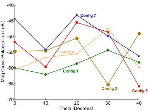
It would be interesting to plot the variation of reflection coefficient phase with respect to the change in the incidence. The variation of phase results of TE00 mode with the change in the incidence angle can be seen in Figure I.17. It can be seen that for certain configurations the variation of phase is over a much larger range than the others. The direction of the phase change for each configuration is indicated by the grey arrows.
Figure I.17: Variation of the magnitude of S12 with respect to the incidence angle.
The coupling between the modes TE00 and TM00 gives the measure of cross-polarization component of the back-scattered field. The magnitude of S12 is plotted in Figure I.18 for five different configurations. It is apparent from the results that the inter-modal coupling is very small (lower than -40dB) for all configurations and for all incidence angles in φ=0º plane.
0 10 20 30 40 -70 -65 -60 -55 -50 -45 -40 Theta (Degrees) M a g Cr o s s -Po la ri z at ion ( dB ) Config 9 Config 5 Config 7 Config 1 Config 2
50
I.4. CONCLUSIONS
In this chapter we have presented the underlying theory of the Scale-changing Technique and explained certain concepts involved in the application of this technique to the planar structures. It has been shown that the Scale-changing Technique is particularly suited for the applications that require large complex planar geometries with patterns varying over a wide range. The concept of scale-changing network to model electromagnetic coupling between adjacent scale-levels is introduced and it is shown that the computation of these SCNs is mutually independent. This formulation, by its very nature is highly parallelizable, which gives SCT a huge advantage over other techniques that have to be adapted for distributed processing.
In the second half of this chapter the Scale-changing technique is applied to the case of a typical reflector cell under infinite array conditions. The results for the phase-shift introduced to a linearly polarized plane-wave under both normal and oblique incidence are calculated and compared to the results obtained by another simulation tool. The good agreement between the results demonstrates that SCT is a reliable design and simulation technique.
SECTION II:
ELECTROMAGNETIC MODELING
USING SCALE-CHANGING
52
II.1. INTRODUCTION
In the previous section we have detailed the underlying theory and working of scale-changing technique with the example of passive reflector under infinite array conditions. In this section we will see how this technique can be used to efficiently model large arrays of non-uniform geometry.
First of all we will introduce the concept of a bifurcation multipole which is essentially a scale-changing network to model the electromagnetic coupling between neighboring cells in an array. Mutual coupling between two planar dipoles will be characterized with the help of this scale-changing network and it will be demonstrated that in the case of a planar dipole array the mutual coupling effect is accurately taken into account when modeled using SCT. Later we will use the bifurcation scale-changing network to compute the surface impedances of 1-D arrays of metallic strips and patches inside a parallel plate waveguide. A comparison of simulation-times with that of conventional techniques will be made to emphasize the efficiency of SCT.
53
Later in the section, the concept of this bifurcation scale-changing network is enhanced to incorporate the mutual coupling in 2-D arrays. Large non-uniform planar array structures are analyzed for plane-wave scattering problem and a good agreement is obtained with the simulation results of conventional simulation tools. Later these structures are analyzed using pyramidal horn as an excitation source. Results are presented for two source configurations i.e. when the source horn is placed at a vertical distance from the centre of the array and when the horn is placed at an offset with an angle of incidence. A comparison of simulation times is given for each case.
54
II.2. MODELING OF INTER-CELLULAR COUPLING
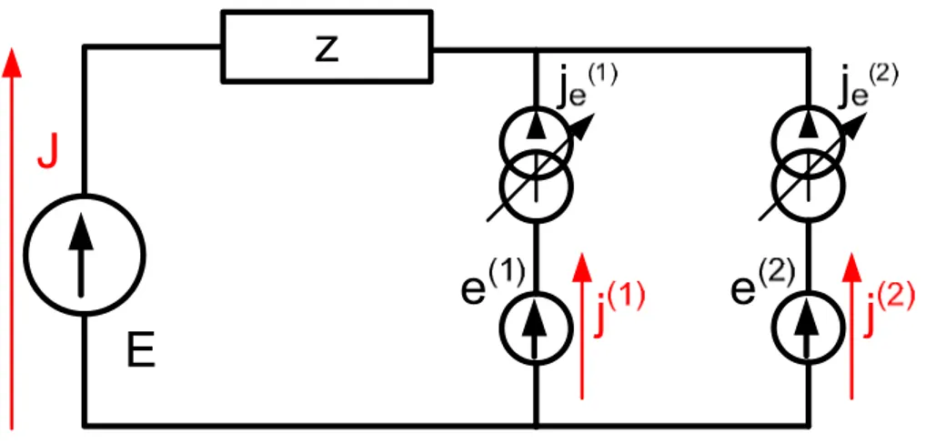
II.2.1. Bifurcation Scale-changing Network
Consider a small array of two unit-cells placed side by side horizontally. Each of the unit-cells can be characterized independently by its surface-impedance matrix (SIM) using an ortho-normal modal-basis defined on unit-cell’s domain. To model the overall behavior of this simple two-cell array, mutual electromagnetic interactions between the cells have to be taken into account. These mutual interactions are characterized by a scale-changing network which when cascaded with the surface impedance matrices of individual unit-cells will give the overall surface impedance or admittance that characterizes this array. The parent-domain Ω0 along with the sub-domains Ω1 and Ω2 (unit-cell domains) can be visualized as the openings of a bifurcated waveguide as shown in Figure II.1, the scale-changing network multipole is therefore dubbed as the bifurcation multipole.
Figure II.1: Electromagnetic coupling between two adjacent unit-cell domains D1 and D2 modeled by a waveguide bifurcation. Inter-modal coupling between parent domain D0 and daughter domains D1 and D2 can be represented by a bifurcation Scale-changing network.
55
Note that in the case of a linear array (unit-cells arranged in one dimension) of non-uniform cells, electromagnetic modeling of an entire array is a simple iterative cascade of the bifurcation scale-changing networks as shown in the Figure II.2.
Figure II.2: Cascade of Bifurcation Multipoles to model the mutual coupling of a linear array.
II.2.1.1. Equivalent Circuit Diagram:
The equivalent circuit to compute the bifurcation scale-changing network between a generic scale s and its subsequent scale s-1 is represented in Figure II.3. Electromagnetic sources forming the two branches of the circuit model the transverse fields in the two sub-domains lying at scale s-1. The source part of the circuit represents the excitation electromagnetic fields of scale-level s as described in Section-I of this thesis.
56
The current sources je(1) and je(2) are the virtual-sources defined in the aperture domains to model the perfect dielectric boundary conditions. The electric field scale-changing sources e(1) and e(2) on the other hand represent the tangential electromagnetic fields in the aperture domains. The tangential electromagnetic field in the parent domain D0 (at scale s) is represented by the source E. Virtual sources and the scale-changing sources when defined in the same domain and using the same modal-basis can be modeled by a single equivalent source [PerretTh Pg-27]. This simplification reduces the analytical calculations of the circuit. A simplified version of equivalent circuit is thus shown in Figure II.4 with the new equivalent current sources j(1) and j(2).
Figure II.3: Equivalent circuit diagram of a bifurcation Scale-changing Network. The dual quantities are shown in red.
Assuming N1 active modes in D0 and N2 in each of the daughter domains (D1, D2) we can express the electromagnetic field quantities in terms of mathematical equations written using the equivalent circuit of Figure II.4.
∑
∑
(II.1)
is the orthogonal modal-basis defined in D
0. Similarly,
57
where Zn is the equivalent parallel modal impedance in the two half-regions. For example, if we have two different substrates at the two sides of the discontinuity plane, assuming air on one side and a dielectric with relative permittivity on the other, modal impedance of the nth passive mode Zn is the parallel equivalent of modal impedances of that mode in each of the dielectric domain and is written as:
(II.3)
Figure II.4: Simplified Equivalent circuit. Virtual source and the scale-changing source of each branch (when defined in the same domain and using same orthogonal modal-basis) can be replaced by a single current source.
and are the column vectors of size 1 listing the coefficients of equation II.1.
(II.4)
Considering the modal-basis and in the two sub-domains the tangential fields in them can be expressed on their respective modal-basis. For sub-domain D1
∑ ∑ (II.5)