Any correspondence concerning this service should be sent to the repository administrator:
[email protected]
To link to this article:
http://www.rmt.univcasa.ma/RMT4.pdf
This is an author-deposited version published in:
http://oatao.univ-toulouse.fr/
Eprints ID: 8331
To cite this version:
Dienot, Jean-Marc Investigations on electromagnetic noises and interactions in
electronic architectures : a tutorial case on a mobile system. (2012)
Mediterranean Telecommunications Journal .
O
pen
A
rchive
T
oulouse
A
rchive
O
uverte (
OATAO
)
OATAO is an open access repository that collects the work of Toulouse researchers and
makes it freely available over the web where possible.
I
NVESTIGATIONS ON E
INTERACTIONS IN ELECTRONI
A TUTORIAL
Abstract: Electromagnetic interactions become critic in embedded and smart electronic structures. The
electronic performances confined in a finite volume
for mobile applications defines new electromagnetic environment and compatibility configurations
canonical demonstrators developed for tutorials and EMC experiences, this paper present basic principles and experimental techniques to investigate and control severe interferences. Some issues are reviewed actual and future scientific challenges for EMC circuit level.
Keywords: Electromagnetic Compatibility, Emission Susceptibility, Immunity, Noise, Aggression, Printed Circuit Board (PCB), Wire, Packaging, Near
1 INTRODUCTION TO THE EMI DOMAIN
1.1 The EMC merging and issues
The domain of the Electromagnetic Compatibility (EMC) still keeps a confidential view in its real and
even if the term has continuously enforced the minds electronics approach since 1996. From this date, a focus on EMC has merged due to official R
Standardizations announcements, for major electronic systems to be on the European and International
Industrials designers and providers first have been seriously alerted on the lack of information and solution
to Electromagnetic Interferences (EMI) standardization comply their products [2]. In fact, the electronic parasitic, interferences, electromagnetic noises and
always been a problem, either due by natural sources (thunderbolt, earth or cosmic radiations)
sources initiated by the start and progress
electric energy for human activities. But with continuous
progress in technology of electronics
performances are boosted in speed, frequency
integration densities, and energy efficiency
electromagnetic coupling's conditions and have been enforced in all categories of electronic
applications[3]. The term “Compatibility” has been associated at “Electromagnetic” since the 1950
with the Silicon Transistor revolution illustrated by “Moore Law”: frequency and number of transistor increase exponentially each year. The EMC dedicated to optimize the best nominal electronics, in presence of different
NVESTIGATIONS ON ELECTROMAGNETIC NOISES AND
ACTIONS IN ELECTRONIC ARCHITECTURE
A TUTORIAL CASE ON A MOBILE SYSTEM
Jean-Marc DIENOT
University P. Sabatier, Francebecome critic in electronic structures. The increase of confined in a finite volume or support defines new electromagnetic nd compatibility configurations (EMC). With eloped for tutorials and EMC basic principles and and control these interferences. Some issues are reviewed to present for EMC at electronic
Emission, Coupling, Noise, Aggression, Embedded, Chip, ackaging, Near-field, TEM.
DOMAIN
The domain of the Electromagnetic Compatibility (EMC) still keeps a confidential view in its real and practical use, even if the term has continuously enforced the minds in the electronics approach since 1996. From this date, a focus on official Regulations and , for major electronic and International market [1]. Industrials designers and providers first have been seriously and solutions to respond Interferences (EMI) standardization to he electronic parasitic, electromagnetic noises and couplings have by natural sources (thunderbolt, earth or cosmic radiations) or by artificial and progress in the control of But with continuous
tronics, whereas
frequency bandwidth,
energy efficiency,the
conditions and cohabitations of electronic levels and ility” has been lectromagnetic” since the 1950-1960 years, illustrated by the requency and number of transistor should EMC philosophy is the best nominal behavior of t electromagnetic
environment. In 1996, it was difficult to give and useful responses to different actors suddenly conc by this problematic: industrials for the standard application, engineers and searcher
students, technicians to validate investigations and measurements. Scientific, technical and theoretical efforts in these ways have been in
nowadays a formal scientific and professional
in EMC domain [4][5][6]. Three fundamental principles the base to consider intellect
EMC studies [7]:
1 - Electromagnetic interferences and couplings are determinist origin, and can have some physicals and electronically explanations to highlight
2 -The EM problems appear in the modes of systems and devices environment has to be considered as
3 -EMC view and approach is a very good exercise that can reflect the understand
the conception quality of any electronic
1.2 The EMC investigation
To start an EMC investigation challenge,
complexity of a device, studies must be driven with three fundamental dedicated formalisms
1: An electronic device or
source. The source is the term that qualifies the device as a
voluntary or involuntary (parasitic) excitations. An electronic device or considered as a victim, that qualifies unwanted and disturbing
involuntary signals arriving to its different the source and the victim, the
link mode. This one is not wanted or designed for, but can
be identified either with wired both.
Fig. 1: The first EMC formalism
NOISES AND
C ARCHITECTURES
:
n 1996, it was difficult to give instantaneous and useful responses to different actors suddenly concerned industrials for the standard’s and searchers for good conception, technicians to validate investigations and Scientific, technical and theoretical efforts been initiated and has generated scientific and professional community Three fundamental principles are consider intellectual and practical approach of lectromagnetic interferences and couplings are origin, and can have some physicals and
to highlight.
appear in the real normal and nominal systems and devices. So the closed and global
has to be considered as a main contributor. EMC view and approach is a very good scientific
understanding, the design and any electronic architecture.
investigation methodology
To start an EMC investigation challenge, among the studies must be driven with three formalisms [3][6][8]:
n electronic device or system can be considered as a term that qualifies the device as a (parasitic) generator of signals and n electronic device or system can be also qualifies the device to present unwanted and disturbing reactions to voluntary or involuntary signals arriving to its different access. Between he key term is the coupling or not wanted or designed for, but can wired or wireless configuration, or
In the first case, the conductive co
transmission line characteristics: characteristic impedance electrical length, have to be considered. In the second case, the electromagnetic and physical characteristics:
permittivity ε, permeability µ, distance, near have to be considered.
2: If a system is considered as a source,
key term of its characteristics [3][6][12]. Emission are presented with the power in Watts (W) or in (dB), or usually in alternative reference to 1 log (P/1mW). If the impedance of the receiver known, emissions can also be represented derivative physicals values:
Tab. 1: The second EMC formalism: physical values for
The emission figure give information on noise repartition over a range of frequency emission margins can be defined by a shift maximums peaks of the real emission diagram.
If a system is considered as a victim, susceptibility
immunity are the key terms for characterizing
sensitivity of device to electromagnetic aggression. Susceptibility is the physical reaction to an aggression. Immunity is the ability of the device to stay insensible to one or multiple aggressions with a certain margin over the
real reaction of the device. The figure of
susceptibility/immunity is derived by placing the levels of aggression that generate a default or dysfunction
the equivalent frequency bandwidth.
Fig. 2: The second EMC formalism: emission, immunity and EMC margins
In the first case, the conductive connections and characteristic impedance, n the second case, the electromagnetic and physical characteristics: materials, , distance, near-field, far field
d as a source, emission is the . Emission levels W) or in Decibel y in alternative reference to 1mW: dBm =10 ance of the receiver or wave is represented with the
EMC representation
give information on electromagnetic repartition over a range of frequency. Then, the can be defined by a shift in dB over the ks of the real emission diagram.
susceptibility and characterizing the sensitivity of device to electromagnetic aggression. Susceptibility is the physical reaction to an aggression. nity is the ability of the device to stay insensible to with a certain margin over the
The figure of
acing the levels of dysfunction, among
immunity and EMC margins
3: conducted and radiated modes
behavior in electronics and the equivalent wavelength to the notion of conducted and radiated modes
physical assumptions, derived from Maxwell equations resume that:
a voltage(V) generates an E versa
a current (A) generates a magnetic field (A/m) and vice versa.
The fundamental key of
wavelength, depending of the frequency electromagnetic waves:
With v: electromagnetic wave speed, in meter/second
λ: Wavelength in meter f: frequency in Hertz
Thus the equivalent electric length is approximated by the ratio of λ/10. If a conductive structure or
dimensions under this value
propagation is considered as mainly conductive and quasi static. If a conductive structure or device
over λ/10, the mode of coupling is considered as mainly radiated and propagative. An ef
radiated power is considered for dimensions of case of radiated mode, the approximated give the distance or the radius
that is called the near-field/far In the near-field radiated mode,
localized by its sources, and is either most magnetic most electric. The impedance wave:
among the distance or radius from the source In the far-field radiated mode: the sour punctual, the impedance wave
in the air, far-field impedance is about
To resume, frequency is a key factor for distinguish different modes of couplings and propagation perturbations and EM signals.
developers, and state of the standards give repartition of these modes:
Tab. 2: The 3rd formalism: EMC
! ! ! " # $ %&' ()* ""#" $ %#" $ '+,-% ()* $ " & ,-%()*&.% )* #%! .%&.%% )* %#! ' .%% )*&. /)* ' #%! ' . /)*&.% /)* ' # %! '
onducted and radiated modes[3][6][12]: the dynamic in electronics and the equivalent wavelength rely notion of conducted and radiated modes. Some basic physical assumptions, derived from Maxwell equations, Electric Field(V/m) and vice -current (A) generates a magnetic field (A/m) and vice
key of these generations is the depending of the frequency and the speed of
Eq. 1
v: electromagnetic wave speed, in meter/second in meter
Hertz
the equivalent electric length is approximated by the . If a conductive structure or device has this value, the mode of coupling or propagation is considered as mainly conductive and
quasi-If a conductive structure or device has dimensions the mode of coupling is considered as mainly An efficient configuration of radiated power is considered for dimensions of λ/4. In the the approximated number λ / (2 ) give the distance or the radius from the source to outside,
field/far-field frontier(NFF).
mode, the electromagnetic field is , and is either most magnetic most
pedance wave: in ohms, vary
among the distance or radius from the source.
mode: the source is considered as
he impedance wave Zw is constant. For remind,
impedance is about Zw = 377 Ohms.
, frequency is a key factor for distinguish different modes of couplings and propagation of and EM signals. EMC engineers and nd state of the standards give a technical
EMC frequency range of investigation 0 ( )' * + ,) ' ' -'- ./- ( )' 0 * + ,) ' ( )' 1 - 2 3 4/ -/ ./ -' ' -' ,)/ - / -' +-( )' 1 5 2- 2 4/ -/ / +-4/ -/ 46 4/ -/ 46 / */5 # %! ' - 2 + ,) ' */54/ -/
1.3 The EM environment of electronics architectures
Since 30 years, electronic architectures and applications are diffused in all sectors of public and daily life:
phones, Portable Electronic Devices(PED), public and personal network, Wireless and Power Line Current(PLC) Communication technology, Electronics in Car
and comfort, Smart Mobile systems(personal robots This development leads to increase electroma pollution and electromagnetic field's interactions and inside system [13][14][17]. Independently of necessary EMC standardization to provide compliant products on commercial and public market
risk of different couplings scenarios and default in system increasing. EMC studies have to been leaded to different parts among the sizes and the "bricks" constituting a system,.
Tab. 3: EMC levels of investigations on electronics
EMC has become critical at Printed Circuit Board and semiconductor integrated chips levels[8]
parts actually are the main contributors of EMC sources victims. We have to deal with more complex
technology and design. The increase of performances: high bandwidth, high speed switching time, low power consumption is a major cause of arise of EM
[10][13].
Fig. 3: EMC trends of electronic technologies
The packaging and PCB are the interfaces
from active devices and their loads or function. complexity and density of integration of these structures generate also new complex EM configurations that radiate or receive more efficiency disturbances. If
generated in these structures or coming from outside have large wavelength, the main behavior of PCB is considered
.%%/)* ) .% /)* ) ./)* ) .%% )* ) .% )* , ,% ,% , ,% 1-%2 13- 13- 1- 13-,-'3,2 ,3-' ,3-' ,-3', ,3-' ,%%2 , , ,% , & 4 5 !4 5" 4 ( 6 !6 " 4 0 !4 0" 0 6/# 7 7 7 7 of electronics
electronic architectures and applications are diffused in all sectors of public and daily life: Mobile able Electronic Devices(PED), public and Wireless and Power Line Current(PLC) Electronics in Car for security (personal robots), etc… This development leads to increase electromagnetic interactions outside Independently of the necessary EMC standardization to provide compliant products on commercial and public market, the physical
scenarios and default in system is EMC studies have to been leaded to different parts among the sizes and the "bricks" constituting a
EMC levels of investigations on electronics
EMC has become critical at Printed Circuit Board (PCB) [8][9][12]. These EMC sources and more complex active chip's The increase of performances: high-, high speed switching timehigh-, low power
arise of EM interactions
EMC trends of electronic technologies
faces and supports oads or function. The complexity and density of integration of these structures EM configurations that radiate If a perturbation structures or coming from outside have rge wavelength, the main behavior of PCB is considered
as conducted. The major part of EMC consideration common mode disturbance that
numerous actual non-ideal common mode connections packaging. For others cases, wavelen
same dimension as actual PCB and connections, that define them as radiator sources or victim
Fig. 4: Synthesize of EMC
2 EMI IN MOBILE
ARCHITECTURES
2.1 Definition of a mobile/embedded system
Electronic has acquired new challenges since
embedded systems leads to new kind of applications and innovations. A definition of embedded/mobile system “A mobile or transport system using a range o electrical and electronic functions to realize tasks with autonomous and robust conditions” level, this concept derives new
trend to compliances issues[15]
-Precise and critical choice of technology of circuits and sub-systems optimized to keep performances
-Physical constraints as inter reduced volumes and weight, optimized
-Electrical energy that is limited in the time and informations that have to be operational in all conditions
Fig. 5: The different electronics' functions
Consequently, it’s the main point of view of this Electromagnetic interactions
new views and approaches for
electromagnetic risk is enforced with these applications, and the EMC solutions to prevent them
these specific constraints, for example
) . )* .%%()* ,%% ,( 1- 1-% ,-3', ,-'3, ,% ,%% 8 7 06 #86 7 90 6 69# 7994 06 #86 7 90 #8 6#8 47 # 4 68 #
as conducted. The major part of EMC consideration is the disturbance that unfortunately benefit of ideal common mode connections and , wavelengths are mainly in the as actual PCB and connections, that define m as radiator sources or victim[14].
EMC behaviors on PCB
IN MOBILE ELECTRONICS
Definition of a mobile/embedded system
has acquired new challenges since the notion of leads to new kind of applications and ition of embedded/mobile system: “A mobile or transport system using a range of limited
functions to realize one or more tasks with autonomous and robust conditions”. At circuit new constraints for designers to [15][17]:
choice of technology of circuits and to keep performances
Physical constraints as inter-connections of subsystems, reduced volumes and weight, optimized dimensions.
that is limited in the time and electronic s that have to be operational in all conditions.
functions in a Mobile/Embedded system
Consequently, it’s the main point of view of this paper: and compatibility have also for investigations. The notion of risk is enforced with these applications, and the EMC solutions to prevent them must be adapted to
, for example: 06 #86 7 90 9 9# 90 #8 9 9# 90 6 69#
-Avoid shielding or protections devices that complexes the system
-Find the EM compliances that stay valid in function mobile conditions and in time
-Find EM protection solution that can be
(software’s protection)
2.2 Description of demonstrator EMC investigations
We present a family of mobile system demonstrators for EMC investigations, used both for tutorial and
studies in the plat-form Labceem [54]. The objective is to investigate and analyze main external and internal EM disturbances that can affect an autonomous electric system It consists of motorized autonomous small
and mix different electronic technology. Th are used as a view demonstrators of
designing principles for electric motion. For this tutorial, we focus on demonstrator ROB-CEM I,
about 24cmx35cmx35cm, realized on a wooden weight and EM considerations. It combines elementary electronic techniques used for the electrical motion [16]: Brushless and continuous controlled, Power PCB with MOS/IGBT
integrated drivers, command/control PCB with high CMOS transistors and memory or FPGA technology sensors for speed and position control, o
control and command. The motion and trajectory of the mobile system is controlled by the speed of each wheels. Two commands, PWM01 and PWM00, can be adjusted independently to drive a current in each motor.
rate of a PWM pattern generates an equivalent mean current, with a range of positive to negative value. So a combination of different movements can be
different negative: positive speed of each wheel
Fig. 6: Description of demonstrator ROB-CEM
2.3 Emissions of the global mobile system
For starting the EMC point of view with the emission of the system, the investigation of EM noises and levels of the system consist in three steps:
- Place the system in nominal function - Use an adequate emission sensor or antenna - Use a receiver or spectrum analyzer
representative distribution of emission levels frequency bands 4 : 4 5 5 ! " 1; .-,1 <3= 5 88 > 7 $ ! 4 : 5 ?%, 4 : 5 ?%1
Avoid shielding or protections devices that Find the EM compliances that stay valid in function Find EM protection solution that can be versatile
prototype for
We present a family of mobile system demonstrators for tutorial and research The objective is to nvestigate and analyze main external and internal EM disturbances that can affect an autonomous electric system systems that use These prototypes of technology and For this tutorial, I, of dimensions on a wooden support for combines different used for the controlled Brushless and continuous current /IGBT transistors and ommand/control PCB with high-speed FPGA technology, , optional Wireless motion and trajectory of the mobile system is controlled by the speed of each wheels. Two commands, PWM01 and PWM00, can be adjusted to drive a current in each motor. The cyclic rate of a PWM pattern generates an equivalent mean e of positive to negative value. So a of different movements can be programmed by
wheel.
CEM I
system
For starting the EMC point of view with the emission of the and levels of the
antenna
that gives the distribution of emission levels on
Fig. 7: Typical radiated electromagnetic field measurement electronic devices and equipment
But, as the global noise of
qualitatively very wide-band and not obviously ranged experiment is not yet always convenient.
identify main fundamental frequency of the functional system, and some harmonics at the te
our system, we have for example a fundamental frequency
of f0=10 kHz, and harmonics distributed until
allows to think to main conduct near-field only radiated emissions electronics parts and they different
a non negligible wide band equivalent noise
of electronic chips and components are in the range to 1 ns, that leads to have equivalent frequencies range from MHz to GHz. So we can attend that
levels are mixed with EM ambient noise, especially in same band of normalized radio frequency as MHz), VHF, UHF, Mobil
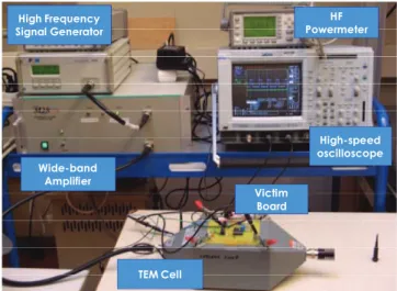
characterization must be conducted in shielded space, with the use of Faraday or anechoic chambers.
at small device, circuits and planar configurations, an alternative exists to these expensive and
shielded TEM mode antenna or
commonly used in some standardization procedures and for pre-qualification and investigations in R&D laboratories. For the precise measurement
wide GTEM Cell. The main constraint is to respect a minima a ratio 1/3 of the distance between system and septum(conducted plate) to respect the TEM mode
Fig. 8: GTEM- Radiated field experiment for electronic devices
,1 <3= 5 88 > ,1 -4 & ,%()* 4 5 ,1 -"# $ ! % 4 : 5 ?%1 /8 !/ 8 & " ≅ ≅ ≅ ≅ .% 0 &,@ /)* ≅ ≅ ≅ ≅ - . 8 ≅≅≅≅ -% ) # 7 & $ 8
ted electromagnetic field measurement setup on electronic devices and equipment
noise of a complex system can be band and not obviously ranged, this experiment is not yet always convenient. A first step is to fundamental frequency of the functional s at the ten or higher rank. For our system, we have for example a fundamental frequency =10 kHz, and harmonics distributed until 150 kHz, that lows to think to main conducted emissions and weak field only radiated emissions. But combination of all different switching’s rate leads to equivalent noise. Switching rate of electronic chips and components are in the range of 1µs to 1 ns, that leads to have equivalent frequencies range from to GHz. So we can attend that the emission peaks and levels are mixed with EM ambient noise, especially in the normalized radio frequency as FM (100 MHz), VHF, UHF, Mobile phone and others. The characterization must be conducted in shielded space, with anechoic chambers. For investigation device, circuits and planar configurations, an exists to these expensive and complex solutions: TEM mode antenna or strip line[18]. They are ome standardization procedures and for stigations in R&D laboratories.
on our demonstrator, we use a . The main constraint is to respect a f the distance between system and septum(conducted plate) to respect the TEM mode[19].
for electronic devices and small systems " .% . ) 4 : * # : ( * -% . ) # 8
We can obtain an emission figure that is pertinent, and confirm the hypothesis on the real wide-band emission peaks as represented in followed figure.
Fig. 9: Radiated electromagnetic field distribution of demonstrator ROB-CEM I
Analyze of the frequency diagram allows understanding and identifying the contributions and radiated sources linked to the architecture of the system:
10kHz/300kHz: Motors and harmonics of Motors 100MHz: Switching rate of Power transistors (MOS, IGBT), 1 to 2 µs
250MHz: Switching rate of power drivers (Power Bipolar Transistors), 100 ns
400/600MHz: Switching rate of CMOS / CPLD, 1ns 800-980 MHz: RF Chips noises (carrier)
2.4 Immunity of the system
The investigation of the immunity and electromagnetic risks consist in three steps:
- Define one or many criteria's default
- Define the type of aggression: harmonic and transient signals, direct (conducted) or near/far field couplings. - Choosing the kind of coupling behaviors with parameters
as frequency, levels, direct or radiated couplings
The immunity investigation is less trivial and more difficult to realize than the emission approach. It could appear a lot of conditions and parameters, and the aggressive character of the investigation can cause complex real defaults, even in out of bandwidth of the system [20]. For our demonstrator, we can focus on some elementary immunity cases:
- The system is mobile, so the aggressions are mainly radiated type and not direct conductive.
- Each part has a range of sensitivity, but the most weak part seems to be the CMOS circuits: they are supplied on low energy (5V) and they have a wider band –with. The mode of couplings depends of elementary parasitic antenna formed by PCB wire and other parts connected. For example, when use of integrated circuits, some pins are unused because the function are not active, or some special control of IC, as Inhibit or Reset. If unused pins or other connections are in open circuit, they present a open loop
that is very favorable to Electric field couplings. If unused pins or connections are connected to the reference's connections of the system, they present an common impedance and a loop conductive surface. So the magnetic field coupling and the generation of voltage among the distance of connection can cause a sufficient energy that enter the circuit and trigger an involuntary switching. In these two cases, you have either electric-capacitive coupling, either magnetic-inductive couplings.
If a far-field illuminate the circuit, as a RF signals of Wireless system, both electric and magnetic fields can couple and disturb the functional integrity of the device To resume, let’s see on three experiment's demonstrations the
qualitative effects of aggression on the prototype[16]:
Fig. 10: Three canonical modes of coupling for radiated immunity
-Electric field coupling is realized by the "hand" effect: a slightly quasi-static shift in the near electric field, around the Reset pin stayed in open circuit, is realized by moving a conductive charged element (the hand or other) close to the pin; the command of one wheel of the system is perturbed and the main consequences is a loss of trajectory and nominal function.
-Magnetic field coupling and effect is visualized by injecting a magnetic field in a loop: to avoid Electric field coupling conditions, the ideal and state of the art is to rely Reset pin and unused pins of device to a reference voltage. But this configuration realizes a closed loop, and with the reference conductor as common impedance, some disturbing current voltages are derived. The aggression is simulated by a ESD (Electrostatic Discharge) that generates both E and H field during triggering. If placed in a normal direction to equivalent surface formed by the closed circuit or wire, a transient current is coupled and is sufficient to trigger once again the Reset function. So the effect and consequence on the circuit is the same than previously. But we feel and see that this aggression is less reproducible and more dependent of orientation than the first case.
-A last case, complementary of the previous ones, is to generate an equivalent established harmonic Field with a RF source, for example a mobile phone nears the command board. The coupling to trigger the Reset is more difficult to establish, because the equivalent density of energy less
# & "' ( & ' ) " * ') "# + ' ') "# +' ,& $ ) * ') "# + ' - $ . / "# $ # & " & '' ??..! ,& $ ∆ / / / / ∆ 8 4 1& ) $ ∆ / / / / ∆ 8 4 .& $ *-( / -( / 7 8 4
intensive and directive than previous cases o Also a "natural" protection is obvious b
tentative of coupling a high frequency signal: the carrier of the RF Source, in the range of 900MHz, 2.4
natural low bandwidth of electronics victims.
conditions, a very common scenario of coupling/immunity can arrive: the envelop detection. Because of inherent presence in PCB and components
capacitance, and junction (semi conductor P
localized or parasitic in electronic devices, we have a involuntary demodulator or peak detector configurati the low frequency timing and pattern of RF Signals can be detected, as the envelope of the RF carrier often used in CW or FM transmission. These conditions
sufficient to trigger once again the Reset or other inputs on circuits, and having a disturbing case of the system.
Fig. 11: Example of envelop detector principle as a parasitic demodulator signal and low frequency conversion signal.
In conclusion, immunity is a more difficult domain to investigate and to resolve, with the pressure that a scenario of coupling and reaction can lead to very serious consequences on the integrity of the behavior of a system. After this presentation of global interactions and susceptibility effects on the system, we will focus on techniques to qualify and evaluate the internal contributions of emission, couplings and immunity cases
3 FOCUS ON EMISSION AND EM NOISE OF ENERGY/POWER MODULES
3.1 The sources and couplings in power structures
We present a canonical prototype that want to behaviors of emissions of switching module
energy conversion and supply in most modern
system[21][22][24]. The demonstrator PCB
representative of an elementary architecture of a power using actual transistors technology as MOS power or IGBT. These components are reported on a PPCB (Power Printed Circuit Board) with some quality for dissipating temperature. Three cases of emission will be pres
Conducted mode, the Near-field mode and the F mode.
ective than previous cases of aggression. Also a "natural" protection is obvious because of the igh frequency signal: the carrier of in the range of 900MHz, 2.4 GHZ and the of electronics victims. But in certain , a very common scenario of coupling/immunity ve: the envelop detection. Because of inherent as resistance, semi conductor P-N), either devices, we have a configuration. So the low frequency timing and pattern of RF Signals can be of the RF carrier often used in These conditions could be Reset or other inputs on disturbing case of the system.
: Example of envelop detector principle as a parasitic demodulator signal and low frequency conversion signal.
In conclusion, immunity is a more difficult domain to e, with the pressure that a scenario of coupling and reaction can lead to very serious consequences on the integrity of the behavior of a system. After this presentation of global interactions and
system, we will focus on main internal contributions at circuit level.
D EM NOISE OF
The sources and couplings in power structures
ype that want to review main of switching module used for
energy conversion and supply in most modern
The demonstrator PCB is
architecture of a power cell, using actual transistors technology as MOS power or IGBT. These components are reported on a PPCB (Power Printed Circuit Board) with some quality for dissipating will be presented: the field mode and the Far field
Fig. 12: Views and description of canonical power PCB demonstrator (PTR_6)
Fig. 13: Transversal view of Power PCB d
3.2 The investigations conducted mode integrity signal
3.2.1 The experiment
Conducted mode and investigations can be realized on main PCB with a wide band oscilloscopes associated to voltages probes and currents probes. A system calibrated at
correct today to have a good conducted characterization both common devices on PCB. Some
nowadays input impedance that can be shi
50 ohms that improve the sensibility and the frequency adaption of the connections. If available, the use of a spectrum analyzer will be more
noise rejection and the frequency resolution. Voltages probes, especially in switching mode characterization must be compensated in frequency. For current probes, i high frequency loop current probes that can be inserted in the PCB[23][24]. 7 -5 8 / -3.7 -3.7 3. ' ' A.-2 0 A ,1-2 A ,B--/ 2 -/ ' ' -
Views and description of canonical power PCB demonstrator (PTR_6)
Transversal view of Power PCB demonstrator PTR6
The investigations conducted mode and
Conducted mode and investigations can be realized on main PCB with a wide band oscilloscopes associated to voltages probes and currents probes. A system calibrated at 1 GHz is correct today to have a good conducted characterization for both common devices on PCB. Some oscilloscopes have impedance that can be shift sometimes on improve the sensibility and the frequency ions. If available, the use of a will be more pertinent for the signal to noise rejection and the frequency resolution. Voltages probes, especially in switching mode characterization must be compensated in frequency. For current probes, it exist high frequency loop current probes that can be inserted in
9 8 3.7 :( ' ' 3.7 -7 -5 / ; * - $ 9 8 - 9 8 / -/ -/ ' ' - .-'/
+-Fig. 14: RF coupling techniques’ for typical conducted EMC testing[25]
3.2.2 Results and parametric behaviors
First conducted results give a view of the real waveforms in different points of the board prototype. Interesting conclusions is the overvoltage on power supply and ground; also the measure of pseudo-oscillation (f = 1,7 MHz) or ∆t of these signals give pertinent information. Main conclusion is that important disturbances are in common mode or impedance: in wire or cable of Power supply, in wires and planes of ground, in radiators on the component and the load, in routing/connecting configurations. The main reduction/optimization of the emissions can be obtained by using adequately bypass/decoupling capacitors or filters, optimizing the ground/supply routing and modifying electrical conditions of the switching [16].
Fig. 15: 4 examples of qualitative reduction of conducted perturbations
3.3 The investigations of Radiated Emission 3.3.1 Near-field radiated mode
Near-field mode characterization is an alternative but complementary method between conducted and far field characterization [26]. In near-field mode, the components of the electromagnetic field have interesting properties or characteristics:
-Magnetic field issue from intensive variations of current ∆I/∆t
- Electric field issue from intensive variations of voltage ∆V/∆t
- Spatial localization and repartition of the field's contributions and origins
-Identification of “hot” spots of high current-low impedance part of the boards, high voltage-high impedance parts of the board.
- Characterization without conductive insertion problem and losses; and independent of the connective access
3.3.2 Near-field radiated characterization [26][28]
Near-field probes are essentially two types: Electric field as a monopole or open-circuit structure and Magnetic Field as a loop or short circuit structure. The high-performances of the near-fields probe are the size resolution linked to the band with. It exists commercial probes, characterized by attenuation factors and other-component field ratio rejection. For particular uses or others performances, it’s possible to design by own near-field probes, with HF coaxial cables or printing on substrates[29][30][31]
Fig. 16: examples of different near-field probes and antennas for EMC testing
The quality of the experiment depends also of the use of rigorous mechanical test fixture, to maintain precisely probes and to shift over a surface keeping a good absolute resolution. So, some supports, motorized or not, moving in X, Y and Z directions, must be associated to Near field probes to obtain pertinent and serious scan figures. In this case, the Near-field experiment has to be driven in all directions, and deal with different Electric or Magnetic fields components: Ex, Ey, Ez and Hx, Hy, Hz.
Fig. 17: example of a near-field scan test bench and fixtures
6/58 ! /" ! " 44 5 ! " ! " 0 " # : : -95 -85 -75 -65 -55 -45 -35 0 25 50 75 100 125 150 175 200 225 ! 8" $ ! )*" 4 ! 5 " ' ," ' & 0 ' C 5# C + , /)* 9: & C ) C + ,@ /)* 4 5 C 9 & & 4 $ C 4 5 * D > E 5 4
Fig. 18: Principles and procedures for 3D near-field testing[32]
3.3.3 Near-field radiated results
As said previously, the E/H scan of the prototype is a confirmation of conductive dynamic behavior. An example of global scan in H-field mode is reported here for the power PPCB with it’s main active chip.
Fig. 19: Examples of global scan figures of power chips and PCB [33]
Some specific zones can be tested precisely, without problem of insertion, so to have qualitatively comparison of different frequency and positions behaviors. For Power PCB, it’s the case of image of high current variation, where H-field probe can show very intensive zone of switching current and equivalent generated frequency resonances. We can have also a comparison of radiated chip behavior, as illustrated in result of our prototype (MOS vs IGBT)
Fig. 20: Examples of specific localized scan figures on pins of power transistors (MOS& IGBT)[34]
3.3.4 Far-field or established-Field mode
To complete emission investigation on the electronic board, characterization of radiated emission can be driven. Here is a review of actual techniques to measure radiated emission on electronic boards[35][36][37] :
Tab. 4: Review of different radiated measurement equipment adapted to components/circuits electronic devices.
As said, TEM cell family is a convenient way to have a representative view of radiation of medium/small electronic structure in alternative to OATS or Chamber measurement. A normalized TEM cell (called Crawford Cell) is used in the official standards for pre-qualifying PCB and Integrated circuit. The TEM cell, uses a strip line configuration that is shielded. The user must realize specific PCB, with following rules:
-Components chips to be characterized mounted on the inside face of the PCB
-Connecting, supply, decoupling, others function and connectors to the outside
-Distance of the chip inside TEM cell and septum must be optimized, that is a minima a ratio of 1/5 à 1/3.
-The Band-with of EM noise attended must be in adaptation with band-width of the TEM cell.
3.3.5 Radiated emission of power chips and PCB with PTR6 demonstrator.
The prototype demonstrator here is a PCB in respect of TEM Cell aperture dimension: 10cm*10 cm
0 C $ $ * $ C * C $ )* $ ) $ )C * 4 7 D > E ) 1 $ ' ( 2 D > E )D )> )E
%3 & ', & ( 04& + "5( . " &$
D
!
"
>! "
63 & ', & ( 04& + "5( . " &$
4 $ )D + * A, D > E 4 : F ! " $ 9 ! " $ 6/58 D > E 4 $ E & * A , 4 : F ! " $ 9 ! " $ 6/58 ! 5 " !)*" ! 5 " !)*" 6 $ < = 9 < >- / - 0 * ' - 3-< 1 0 2 3 '-+-' ;( 8 & :$ " $ < = 9 < >- / - -) ' - ? ;( 3 ,) -/ - 3-< - + / *- 2 3 '-+-' ;( ? - / - + 2 ;( /8 7( = % 9 < 3-< - + / *- 2 ' - / ' @ ;( 1 / 8 - + 7 5-' 8 3-< 0 / / )/ - +/' ( A . < 9 64 B :(C ; '- - / / / ->- / + * / + ,) ' >- / + 5-' -< 7- - ( @ ) / '-+-' '2 -,) D (
Fig. 21: Radiated TEM Cell experiment of Power PCB PTR6
One interest of TEM CELL is that user can design prototype, in respect with conditions of
investigate radiated figures of sequential
The power chip for example, is placed alone in canonical PCB prototypes. So, different technologies of power/smart power chips are tested with
routing, to have a relative comparison of radiated and switching EM noises from different technologies. contributors to excessive emissions can be
linked to different EMC choices.
Fig. 22: 2D/3D views of Radiated TEM Cell experiment of Power PCB PTR6
Measurements are realized commonly to a receiver or spectrum analyzer. In this last case, we can compar identify the impact of the switching conditions on the emission source, and especially rely it to main frequency resonances of the PCB routing and architectures. retrieve same behaviors and frequency peaks either in Near field studies, either in global system analyze observed on Rob-Cem I.
Fig. 23: Comparison of radiated behavior for different Power technologies and electrical conditions [34] 4 , 8 7 !-% 9 " $ ,&- .. ' $ . / 0 !,% 4 4 : 4 5 !=%% &,%% " C 4 5& F & &4 : & * , '# . + 5 .. " ,$. + 9 4 5 6 4 5 $ 4 5 ! " EM Cell experiment of Power PCB PTR6
user can design its own prototype, in respect with conditions of TEM mode, to part of a board. The power chip for example, is placed alone in our different technologies of with a same PCB routing, to have a relative comparison of radiated and noises from different technologies. Main be evaluated and
: 2D/3D views of Radiated TEM Cell experiment of Power PCB PTR6
to a receiver or spectrum analyzer. In this last case, we can compare and identify the impact of the switching conditions on the emission source, and especially rely it to main frequency resonances of the PCB routing and architectures. We retrieve same behaviors and frequency peaks either in
Near-lobal system analyze observed on
Power technologies and
4 FOCUS ON IMMUNITY AND SUCSC
OF ELECTRONIC DEVICES FOR COMMAN
We now review and describe immunity problematic centered on a particular and common victim in a
architecture: the device and PCB used to control and command the system. The immu
of EMC, is considered as a parasitic couplings shift in nominal functions
temporally loss of function. Destructive
considered, but it’s a domain of EMC for the view of intentional aggressions.
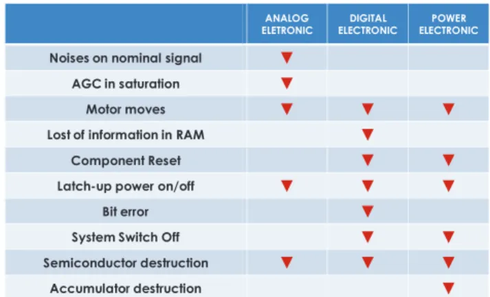
Tab. 5: The main immunity default risk in electronics
4.1 The different architectures of PWM
Pulse Width Modulation has become a major signal pattern for many electronic functions: telecommunications, digital coding, digital modulation, motor command,
active control. PWM signals generations and control are integrated in many electronic complex chips,
µcontrollers. For specific use, especially in mobile, Embedded and Mechatronic applications, designers have to realize and use dedicated ci
command, to respect high level of control of the system. With EMC point of view, PWM
of the main potential victim in the configuration system, and if disturbed by anyway, a major potential of electromagnetic risk with the consequences of loss of function and integrity missions of global mobile system.
4.2 Default criteria’s and conditions.
At electronic chips and semi susceptibility and dysfunction here.
Tab. 6: The main defaults and susceptibility cases
0 !,% &, " 4 1 F 4 : * $ 4 5& ! "
G6#0 9
6 G
0 9 8 7 38 4 :( 7 6 08 > 8 4 ; 7 4 (? 4 0?33 ?6 . 33 ?: 6 :(8 ?: 3 4 = :? 7 384 (8 ?: 4C 3 4 = ; 48 0 7 384 (8 ?: # / 7 $ $ 7 & : $$ 5 : 9$$ Y AND SUCSCEPTIBILITY C DEVICES FOR COMMAND.review and describe immunity problematic particular and common victim in an electronic evice and PCB used to control and The immunity approach by the way a parasitic couplings that occurs a of the system, at least a . Destructive effects are not considered, but it’s a domain of EMC for the view of
The main immunity default risk in electronics
architectures of PWM
Pulse Width Modulation has become a major signal pattern for many electronic functions: telecommunications, digital coding, digital modulation, motor command, and supply PWM signals generations and control are integrated in many electronic complex chips, processor and fic use, especially in mobile, applications, designers have to realize and use dedicated circuits with PWM optimized command, to respect high level of control of the system. With EMC point of view, PWM pattern can be considered of the main potential victim in the configuration system, and if disturbed by anyway, a major potential of risk with the consequences of loss of
missions of global mobile system.
and conditions.
At electronic chips and semi-conductor, many causes of dysfunction have been listed, for example
and susceptibility cases in electronics
D
47
: - -4 + . 6 / 2 -' ' E / / 32) * + ;( (.?3 '2- $-# 79/ 7 8 9#6 06/68 7 7 8 9#6 49 7 8 9#6 H H H H H H H H H H H H H H H H H HIf we focus on PWM signal characteristics, the main susceptibility criteria is the shift of different
parameter of the PWM, that can derive an involunt current which modifies the nominal command.
current wanted is realized by electrical parameters as switching margins, switching supply levels, cyclic
nominal frequency. They can be all defined as default's criteria. Another consideration is the packaging of
chips used for signal generation. As a digital type signal,
others functions and pins associated are often
accompanying the function, as Errors Compensation, Reset, High-level forcing, Watch dog etc… Used or unused, t pins are other ways of default, activated
triggers especially in pulsed parasitic aggression signals. To resume, a review of immunity cases
investigated both in pulsed/transients signals aggression and harmonic wide –band signals
demonstrators presented here.
Tab. 7: Typical types of immunity testing approaches on electronics
4.3 Pulsed/transient mode aggressions 4.3.1 Experimental pulsed aggressions
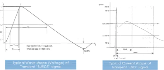
In pulsed mode aggression, different wavefo be used[25][38][39][40].
Fig. 24: Examples of two Transient Aggression signals for immunity testing
The main parameter of the experiment is the peak or means equivalent level of the transient pulsed waveforms that can be linked to equivalent energy or power with the normalized waveforms of aggression used. The coupling mode can either be conducted or radiated. In conducted mode, it’s generally a closed coupling mode by the way of Capacitor or Inductors couplings, or contact aggression in the case of ESD Testing. In this case, the second main parameter is the localization of the injection on the board or device. In radiating mode, an Electric type or Magnetic type
6 8 G $ 046!0 4 : 6 I " ( )' / -' 8 / - 0 * * - F ' - (/ /'- ' ) - 5 6 ( )' / -' 8 / - - 2 * - F ' - ./ -' ' ) - 8 6476# 4/ -/ / -' 0 * * F ' - 8 - + 7 5-' 8 /8 4/ -/ / -' / 3 '-+-' 8 / 0 ( )' 4/ -/ 8 / - ( /' / - */5 4/ -/ / -' ) / - - F ' / - *
If we focus on PWM signal characteristics, the main different waveform's involuntary mean current which modifies the nominal command. The mean realized by electrical parameters as witching margins, switching supply levels, cyclic rate and all defined as default's packaging of device or a digital type signal,
others functions and pins associated are often
the function, as Errors Compensation, Reset, Used or unused, these by unintentional specially in pulsed parasitic aggression signals.
cases have been investigated both in pulsed/transients signals aggression with the PCB
Typical types of immunity testing approaches on electronics
Pulsed/transient mode aggressions aggressions
waveforms shapes can
Examples of two Transient Aggression signals for immunity testing
The main parameter of the experiment is the peak or means equivalent level of the transient pulsed waveforms that can be linked to equivalent energy or power with the normalized waveforms of aggression used. The coupling iated. In conducted mode, it’s generally a closed coupling mode by the way of Capacitor or Inductors couplings, or contact aggression in the case of ESD Testing. In this case, the second main parameter is the localization of the injection on the board or evice. In radiating mode, an Electric type or Magnetic type
antenna can be used, placed at limit of near conditions. Two others parameters are important in these conditions: the distance between the board victim and the source aggression, and the pos
Fig. 25: Pulsed/transient surge
Fig. 26: ESD contact/air immunity experiment
4.3.2 Examples of results on canonical test Board
Special test board reproducing
for mobile system have been developed for immunity tests demonstrations. They illustrate main
and aggression scenarios that can be activated by pulsed aggression waves[41].
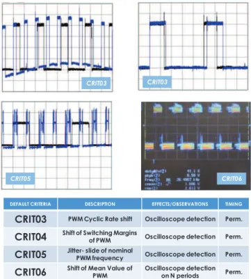
For criteria default named CRIT01, the visualization on oscilloscope of nominal PWM signal and by the activity of a LED helps to validate the criteria, by YES or NO.
For default CRIT02, the very short transient time of activation needs to be visualized at t
one-shot trigger programming to detect the disappearance or appearance of the PWM signals.
0 * * - F ' - (/ /'- ' ) - - 2 * - F ' - ./ -' ' ) - 6/ / / '/ 0 * * F ' - + 7 5-' 8 3-< / * F ' - 7- - 3 '-+-' 8 / ( /' / - */5 / - - 2 / ) / - 9 / + - F ' / - * ) 4 : 4 / 5 / 4 $ 978 / F &,( ,( 43 8 ,% 9 476#/ C 8 8 90 0 5 / 4 7 $ 978 / F &@( @( 43 8 ;% 8 6// 89 8 8 90
antenna can be used, placed at limit of near-field conditions. Two others parameters are important in these conditions: the distance between the board victim and the source aggression, and the position/orientation of the board.
Pulsed/transient surge immunity experiment
: ESD contact/air immunity experiment
Examples of results on canonical test Board
ng a canonical PWM command for mobile system have been developed for immunity tests illustrate main cases of susceptibility that can be activated by pulsed r criteria default named CRIT01, the visualization on oscilloscope of nominal PWM signal and by the activity of a LED helps to validate the criteria, by YES or NO.
For default CRIT02, the very short transient time of activation needs to be visualized at the oscilloscope with shot trigger programming to detect the disappearance or appearance of the PWM signals.
9 6 4 0 # ,1 J 4) #/7 ;% ° 0 869# ,%% 0 0 3 3 &&&&&& 06 ) / 6 ;% ° 0 869# ,%%
Fig. 27: Transient immunity testing on demonstrator PCB(Robcom)
For example, two kind of pulsed aggression experiment are presented
Experiment 1: conducted/near-field by discharge on contact/or closed, with following conditions:
Parameter 1: aggressions points or zones. Here we define 5 Points on the chips and PCB.
Parameter 2: Levels in voltage of Transient/Surge/ESD aggression signals. Here, a range of +/- 2kV.
Tab. 8: Results of Transient immunity testing on demonstrator PCB
Experiment 2 : Radiated pulsed aggression.
The generation of pulsed field can be obtained either by a High transient voltage in a open-circuit, by a High transient current in an low impedance circuit, or both Electric-magnetic field by an ESD discharge in ground connection. Many parameters can be activated for this type of aggression:
Parameter 1: E Field coupling or H-field illumination. Parameter 2: PCB– source distance, typically from 5cm to 2m.
Parameter 3: range of peak level voltage excitation from +/- 8kV centered on 0V
Parameter 4: PCB – source orientations
In the figure, example of results is given, where CRIT01 has been tested with experiment parameters #1, #2 and #3.
Fig. 28: Results of radiated Transient immunity testing on demonstrator PCB
4.4 Harmonic/CW mode aggressions 4.4.1 Experimental test setup
The experimentation consists to illuminate the board with a harmonic CW signals. Either Electric field component or Magnetic field component of the electromagnetic wave generated could be coupled on equivalent high impedance or closed connecting and wires of the system. To confine the aggression and keep reproducibility in experiment, the system has to been protected from outside electromagnetic ambient noise. As for emission concerns, at device electronic level, the alternative of OATS-EM chambers is the use of versatile TEM configuration.
Fig. 29: Harmonic-wave immunity experiment with TEM cell configuration
A high power/wide band amplifier is necessary to be used in conjunction with HF signal generator and Experiment Cell band-widths. The mains parameters of the experiment will be the levels of power injected among the frequency. Another complementary parameter will be the orientation of the PCB/board in the TEM or GTEM Cell, because of the characteristics of equivalent plane wave in the TEM mode that can have different coupling actions. In these case also, many new criteria default can be activated in the same time, so sequential studies can be planned.
Since many years, some pertinent immunity experiments use Reverberation chamber technique[42][43]: a wide band frequency signal is injected in a resonant cavity or chamber
0 0 7 & ' ' "" '' # 1 "" '' 4 8 ,F / 69# E9# 4 6#)65 4 8 4 9 #0, 4 447>, 4 / 9 #01
4 8 1F 768%, 9# $K% &1%% &,( &=%% &=%% &,(
/ 69# 7 7 68%, 9# $ 7 L% M1%% M.%% M@%% M;%% M.%% 0 500 1000 1500 2000 2500 5 8 10 15 20 30 35 40 50 60 80 100 120 140 Couplage H Couplage E 4 ( 7 ! " 4 5& 0 ! " )&$ &$ & & % & 6 ) / & $ ) 4 : ) & 8 5
where a motorized antenna realizes an homogenous repartition of electromagnetic fields and frequency modes. That experiment assumes a complete illumination of a 2D object (PCB) or 3D object(System). In this case, the parameters of immunity test as localization and the main part of the couplings susceptibility modes of an object are entirely excited and tested.
4.4.2 Examples of results on canonical test Board
The dimensions 10x10cm² of Robcom board demonstrator has been planned to be inserted in the TEM Cell. The use of TEM cell allows testing different configurations of technologies. Here, for example, two prototypes assuming the same functions are designed either in double-layer discrete device techniques, either in on layer-SMD technology[41]. We have a difference of routing and wire dimensions sizes to immunity cases comparison.
Fig. 30: View and differences of two different technical realizations of a same functional command board
Complementary default criteria can be used in this experiment, because of the nature of the signal aggression that will reproduce a established permanent aggression. So
some slight susceptibility effects on the PWM
characteristics have to be considered.
Tab. 9: Others defaults and criteria for PWM Signal integrity qualification
For detecting and validate these default(YES/NO), a digital
oscilloscope is necessary, with statistical and
alarms/triggers functions, to help the default hard survey conditions. The level of shift of the different criteria can be nominally fixed to a certain percent (%) of shift from the nominal/non aggressed value, typically for qualitative experiment at 10%. Once one or many default criteria chosen, the experiment is realized with the PCB in TEM cell, with sequential parameters:
Parameter 1: variation of the aggression frequency from Low to High values
Parameter 2: Variation of aggressions levels, in W or dBm, from low to high values
Parameter 3: Orientations of the board depending of septum geometry of the TEM Cell
Fig. 31: View of different orientations of PCB for Immunity TEM cell testing
(Parameter #3).
Synthesizes of results for 1GHz test on boards are presented. That shows the difference and the importance of criteria's choice to a rigorous susceptibility investigation and conclusions at electronic device and PCB levels.
Fig. 32: Comparative results of Immunity testing of demonstrator PCB with harmonic-TEM mode aggression forCRIT#03 to CRIT#06. LAYOUT ROBCOM_B 1 cm LAYOUT ROBCOM_C(MS) 1 cm
# ,+#5# . " * . , + , ( " , 3 * " - 3/ , + 0 78 68 6 0 64869# 8 95 869# 86 6#/ 68%. 4 $ 9 4 3 68%; $ $ :$ 4 9 4 3 68%- N 4 & $ $ 9 4 3 68%= $ $ 4 $ 9 # 4 3 6 8 9 6 $ ,& :&& :
°
; °
%< °
= °
% $ ,& :&& : 0 5 10 15 20 25 30 35 40 45 0 200 400 600 800 1000 1200CRIT03 CRIT04 CRIT05 CRIT06
! )*" 4 : ! 5 " & & %

![Fig. 18: Principles and procedures for 3D near-field testing[32]](https://thumb-eu.123doks.com/thumbv2/123doknet/3622859.106459/9.892.478.846.82.328/fig-principles-procedures-d-near-field-testing.webp)