HAL Id: hal-01544248
https://hal-univ-rennes1.archives-ouvertes.fr/hal-01544248
Submitted on 27 Jun 2018
HAL is a multi-disciplinary open access
archive for the deposit and dissemination of
sci-entific research documents, whether they are
pub-lished or not. The documents may come from
teaching and research institutions in France or
abroad, or from public or private research centers.
L’archive ouverte pluridisciplinaire HAL, est
destinée au dépôt et à la diffusion de documents
scientifiques de niveau recherche, publiés ou non,
émanant des établissements d’enseignement et de
recherche français ou étrangers, des laboratoires
publics ou privés.
Distributed under a Creative Commons Attribution| 4.0 International License
optimization of RF sputtered chalcogenide thin films
devoted to environmental optical sensors
E. Baudet, M. Sergent, P. Němec, C. Cardinaud, E. Rinnert, Karine Michel,
L. Jouany, B. Bureau, Virginie Nazabal
To cite this version:
E. Baudet, M. Sergent, P. Němec, C. Cardinaud, E. Rinnert, et al.. Experimental design approach
for deposition optimization of RF sputtered chalcogenide thin films devoted to environmental optical
sensors. Scientific Reports, Nature Publishing Group, 2017, 7 (1), pp.3500.
�10.1038/s41598-017-03678-w�. �hal-01544248�
Experimental design approach
for deposition optimization of RF
sputtered chalcogenide thin films
devoted to environmental optical
sensors
E. Baudet
1, M. Sergent
2, P. Němec
3, C. Cardinaud
4, E. Rinnert
5, K. Michel
6, L. Jouany
1, B.
Bureau
1& V. Nazabal
1,3The development of the optical bio-chemical sensing technology is an extremely important scientific and technological issue for diagnosis and monitoring of diseases, control of industrial processes, environmental detection of air and water pollutants. Owing to their distinctive features, chalcogenide amorphous thin films represent a keystone in the manufacture of middle infrared integrated optical devices for a sensitive detection of biological or environmental variations. Since the chalcogenide thin films characteristics, i.e. stoichiometric conformity, structure, roughness or optical properties can be affected by the growth process, the choice and control of the deposition method is crucial. An approach based on the experimental design is undoubtedly a way to be explored allowing fast optimization of chalcogenide film deposition by means of radio frequency sputtering process. Argon (Ar) pressure, working power and deposition time were selected as potentially the most influential factors among all possible. The experimental design analysis confirms the great influence of the Ar pressure on studied responses: chemical composition, refractive index in near-IR (1.55 µm) and middle infrared (6.3 and 7.7 µm), band-gap energy, deposition rate and surface roughness. Depending on the intended application and therefore desired thin film characteristics, mappings of the experimental design meaningfully help to select suitable deposition parameters.
The mid-infrared (mid-IR) spectral range is a key region for a large number of applications in diverse areas such as biology and medicine, molecular spectroscopy, ground based and space borne environmental monitoring but also an important issue of instrumentation for astronomy and astrophysics to achieve complex but very reliable instruments1–6. Most infrared signatures or “fingerprints” (fundamental transitions) of organic species and
bio-molecules are essentially located in this spectral window4. Thus, the infrared spectroscopy is a powerful tool for
detecting and determining the composition of complex samples; it is a simple, reliable, fast, cost-efficient and non-destructive method. The development of an optical bio-chemical sensing technology for measurement in real-time is an extremely important scientific and technological issue for the diagnosis and monitoring of dis-eases, drug discovery, proteomics, industrial process control, environmental detection of pollutants or biological agents. Such sensors require a high stability, a high selectivity to interfering molecules and a large detection range to their improve performance. These optical sensors can be based on the existence of the evanescent field which is a fraction of the guided light that is outside the waveguide and thus can probe the external medium surrounding
1Institut des Sciences Chimiques de Rennes, UMR-CNRS 6226, Université de Rennes 1, 35042, Rennes, France. 2Aix Marseille Université, LISA EA4672, Campus scientifique de Saint Jérôme, 13397, Marseille, France. 3Department of Graphic Arts and Photophysics, Faculty of Chemical Technology, University of Pardubice, Studentska 573, 53210, Pardubice, Czech Republic. 4Institut des matériaux Jean Rouxel (IMN) UMR 6502, Université de Nantes, CNRS, 44322, Nantes Cedex 3, France. 5IFREMER, Laboratoire Détection, Capteurs et Mesures, Dpt. Recherches et Développements Technologiques, 29280, Plouzané, France. 6BRGM, Direction Eau, Environnement et Ecotechnologies, Unité Bio-Géochimie environnementale et qualité de l’Eau, 45060, Orléans, France. Correspondence and requests for materials should be addressed to V.N. (email: [email protected]) Received: 11 November 2016
Accepted: 3 May 2017 Published: xx xx xxxx
the waveguide at about a few hundred nanometers. That implies, considering the intrinsic characteristics of the optical sensors, the evanescent field is sensitive to the changes induced by the analyte on the sensor surface such as scattering, fluorescence and notably absorption. Then, it is crucial to be able to work at the extension toward IR waveguides, where chalcogenide glasses provide promising properties. Chalcogenide glasses provide specific optical characteristics (broad mid-IR transparency window, low phonon energies, large linear and nonlinear index of refraction) which make them appropriate to be used in integrated optical devices for a sensitive detection of biological or environmental variations4, 7–11. Amorphous chalcogenides allow light control at very small scales
and are suitable for high index contrast photonic devices, with a compact design requiring a small space and can also be deposited on various substrates12–14. The fabrication of chalcogenide thin films for developing integrated
optical devices is usually carried out using chemical vapor deposition15, thermal evaporation16–18, pulsed laser
deposition (PLD)19–23, or radio frequency (RF) sputtering14, 24–26.
Since the thin film characteristics, i.e. stoichiometric conformity, morphology, topography, structure, or opti-cal properties can be affected by the deposition process; the choice of the deposition technique is decisive. Based on our own experience comparing different physical deposition techniques like PLD, evaporation or RF sputter-ing27–30 and recently published results31–33, it appears that the RF sputtering is a method of choice for photonics
development. Consequently, in this study the RF magnetron sputtering was chosen for chalcogenide layer dep-osition devoted to mid-IR sensor due to the aptitude of a quite good adherence, high compdep-osition control, good homogeneity and uniformity and industrial process transfer prospect. However, as mentioned in the literature31, 34,
the sputtering deposition parameters must be extremely well controlled to prevent a chalcogenide film growth with an unsuitable morphology and topography that can dramatically increase the optical losses of chalcogenide waveguide or can considerably modify the film surface which could affect their functionalization required for a selective and sensitive detection4, 11, 35.
Indeed, to develop an optical integrated system for mid-IR sensors which requires precise opto-geometric characteristics of the chalcogenide layers10, it is essential to adequately determine the influence of deposition
parameters. By the role discrimination of each factor and their possible correlation, it will be possible to control thin film characteristics such as thickness, refractive index, roughness, or chemical composition. The approach based on the experimental design is undoubtedly a way to be explored allowing fast optimization of chalcogenide glasses deposition by means of Physical Vapor Deposition (PVD) processes that are used for a thin films growth onto the appropriate substrate.
In the ternary Ge-Sb-Se system, pseudo-binary (GeSe2)100−x(Sb2Se3)x (x = 5, 10, 20, 30, 40, 50 and 60) glasses
were already studied for photonics applications concerning nonlinear optics or sensors10, 11, 35–40. For this study,
two nominal compositions, Ge28.1Sb6.3Se65.6 (x = 10) and Ge12.5Sb25Se62.5 (x = 50), were selected for their excellent
mid-IR transparency, high stability against crystallization and refractive index contrast allowing optical wave-guiding in mid-IR10, 11, 39. The fabrication of these two different chalcogenide films has been optimized by the
experimental design approach in order to fully meet the criteria for producing optical components devoted to optical bio-chemical sensor applications, for which controlling the layer homogeneity is fundamental for thick-nesses of few µm (from 1 to 6 µm).
The experimental design approach was proposed to quantify the relationship between the different thin film characteristics and the input variables while minimizing the number of experiments. The experimental design was defined considering potentially the most influential factors that are worthy to be studied. To do this, prelim-inary experiments were performed to assess importance of individual factors and to fix the most important ones for the experimental design analysis. The aim of this work is to reveal significant experiments among their large set to determine a connection between deposition parameters and thin films characteristics35, 38. Thus, this study
shows interactions between deposition parameters and determines the main deposition parameters influencing selenide thin films properties. Three input variables or factors have been selected for their expected significant influence: argon pressure, working power and deposition time (Table 1). Six different responses necessary for the optical waveguide development have been consequently investigated: deposition rate, chemical composition, refractive indices (n) in near-IR and mid-IR, band-gap energy, and surface roughness. The knowledge of the dep-osition parameters influence on the mentioned responses will consequently allow achieving accurate manufac-turing of the optical waveguide proposed for the mid-IR environmental sensor working in the range of 3–12 µm.
Results and Discussion
In order to determine the optimal conditions for the film deposition parameters, an experimental design study was carried out. This approach proposes to realize the most significant experiments to obtain the maximum information on the characteristics of the thin films obtained from Ge28.1Sb6.3Se65.6 and Ge12.5Sb25Se62.5 glass targets.
For this study, response surface methodology (RSM) was proposed to evaluate the influence of the factors and to optimize the deposition parameters. In RSM, an empirical mathematical model is postulated to express the response as a function of studied parameters and then to predict responses in the whole domain of interest. In this case, the second order polynomial model was postulated to capture the possible nonlinear effects and curvature in the domain (Equation 1):
= + + + + + + + + +
Y b0 b X1 1 b X2 2 b X3 3 b X11 12 b X22 22 b X33 32 b X X12 1 2 b X X13 1 3 b X X23 2 3 (1) where Y is the response, Xi are the dimensionless variables, bi are the model coefficients. To estimate at best the
coefficients of this model, different designs of experiments are possible and an uniform shell Doehlert41 design
was chosen. This design consists of thirteen distinct experiments; the center point was replicated four times (n° 13 to 16, Table 2) to evaluate the repeatability of the data and to calculate the variance of the experimental error. The Doehlert design is considered as an asymmetrical design, giving different number of levels to the factors: five, seven and three values. The three key factors (X1 is Ar pressure, X2 is working power and X3 is deposition
time) with their respective variation domain for the Ge28.1Sb6.3Se65.6 and Ge12.5Sb25Se62.5 thin films deposition are
detailed in Table 1. The Ar working pressure ranged from 5 × 10⁻² to 5 × 10⁻³ mbar. The sputtering power varied
between 10 and 25 W for the Ge28.1Sb6.3Se65.6 target and between 10 and 20 W for the Ge12.5Sb25Se62.5 target. Note
that the working pressure range and the working power were selected considering preliminary experiments of both films’ depositions. Non-selected factors less influential, like the gas flow, were fixed. Required factors for mid-IR sensor development as the nature of the substrate and the target-to-substrate distance were also settled by preliminary experiments. In case of the Ge12.5Sb25Se62.5 glass, the sputtering power is limited as this target is
more fragile than the other one. The deposition time varied from 30 to 160 minutes. Considering these factors, the sixteen experimental conditions corresponding to the Doehlert design (Table 2) were performed for each of two above mentioned compositions.
The Y responses were selected considering their significance for the development of the environmental optical sensor. First of all, the film composition depending on the deposition parameters must be well identified. The chemical composition can have influence on the wettability of the film surface where an apolar and hydropho-bic behavior must be favored, which can be advantageous for the detection of pollutant molecules. The optical properties of the film must be perfectly characterized and controlled in order to manufacture the required optical waveguide. It is especially relevant for a refractive index in the mid-IR where the absorption of the molecules is used for a bio-chemical detection. Moreover, the quality of the waveguide in term of optical losses, for instance, will depend on the roughness or the film. Thus, the dependence of these Y responses upon the different Xi factors,
particularly the deposition time for the two latter cases, should be investigated. From the results for both com-positions (Tables 3 and 4), the coefficients of the respective models were estimated by the least square method with Nemrodw software42. After validation, the different models were used to graphically represent the response
surfaces in the domain of interest (iso-response curves); these response surfaces were used to interpret the results.
Chemical composition.
The chemical composition of the bulk glass targets estimated by energy-dispersive X-ray spectroscopy (EDS) was found to be Ge28.8Sb5.8Se65.4 and Ge12.6Sb24.5Se62.9 in perfect agreement with thetheoretical Ge28.1Sb6.3Se65.6 and Ge12.5Sb25Se62.5 target composition with measurement uncertainty of about ±0.5%.
For the sake of simplicity, the sputtered chalcogenides films will be named in a general way by considering the theoretical compositions of the two targets; i.e. Ge28.1Sb6.3Se65.6 and Ge12.5Sb25Se62.5 thin films. The chemical
com-positions of the sputtered films also estimated by EDS are presented in Tables 3 and 4 showing generally that they are relatively close to the nominal composition of the bulk target depending on the selected factors. To evaluate
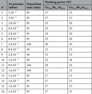
Factors Number of levels Values
Ar pressure (mbar) 5 5.108.9.10−2−3, 2.8.10, 5.10−2−3, 1.6.10−2,
Working power (W)
Ge28.1Sb6.3Se65.6 7 10, 12, 15, 17, 20, 22, 25
Ge12.5Sb25Se62.5 7 10, 12, 13, 15, 16, 18, 20
Deposition time (min) 3 30, 95, 160
Table 1. Domain of the experimental study of Ge28.1Sb6.3Se65.6 and Ge12.5Sb25Se62.5 thin films.
n° Ar pressure (mbar) Deposition time (min)
Working power (W) Ge28.1Sb6.3Se65.6 Ge12.5Sb25Se62.5 1 5.10−2 95 17 15 2 5.10−3 95 17 15 3 2.8.10−2 95 25 20 4 8.9.10−3 95 10 10 5 2.8.10−2 95 10 10 6 8.9.10−3 95 25 20 7 2.8.10−2 160 20 16 8 8.9.10−3 30 15 13 9 2.8.10−2 30 15 13 10 1.6.10−2 30 22 18 11 8.9.10−3 160 20 16 12 1.6.10−2 160 12 12 13 1.6.10−2 95 17 15 14 1.6.10−2 95 17 15 15 1.6.10−2 95 17 15 16 1.6.10−2 95 17 15
Table 2. Experimental parameters of the Ge28.1Sb6.3Se65.6 and Ge12.5Sb25Se62.5 thin films deposition (Ar pressure,
more precisely the influence of the Ar pressure, the deposition time and the working power on the thin film com-position, the variance (ΔGe, ΔSb and ΔSe) of the chemical composition of the thin films compared to the real composition of the bulk glass targets were analyzed.
Ge28.1Sb6.3Se65.6 thin films. Figure 1 shows the chemical composition changes of the films compared to the
tar-get (ΔC = Cfilm(%) − Ctarget(%)). Considering germanium, ΔGe varies from −2.5 to 3.5%. The films can have
a deficit or an excess of germanium compared to stoichiometry but the films present mostly an excess of Ge (average value of ΔGe = 1%, deviation 0.3% in Table 3). Nevertheless, some deposition parameters can lead to a deficiency in germanium content (Fig. 1). In that case for a high Ar pressure and a low to moderate power, a sig-nificant decrease of the response is effectively observed. Thus, the continuous variations of ΔGe can be controlled mainly by varying the pressure of Ar. For a relative high Ar pressure and an intermediate RF power, the thin films
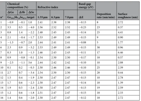
n°
Chemical
composition (%) Refractive index Band-gap energy (eV)
Deposition
rate (nm/min) Surface roughness (nm)
ΔGe ΔSb ΔSe 1.55 µm 6.3 µm 7.8 µm ΔE Ge28.8Sb5.8Se65.4 target 1 −0.9 −0.1 1.0 2.41 2.38 2.38 −0.13 8 2.72 2 3.5 0.5 −4.0 2.56 2.52 2.52 −0.23 23 0.37 3 0.8 1.4 −2.2 2.48 2.45 2.45 −0.14 25 4.41 4 2.1 −0.4 −1.7 2.53 2.49 2.49 −0.15 9 0.90 5 −1.3 −0.7 2.0 2.44 2.41 2.41 −0.08 5 1.77 6 2.3 0.9 −3.2 2.53 2.49 2.49 −0.15 38 0.96 7 0.3 1.0 −1.3 2.46 2.43 2.43 −0.11 17 6.46 8 0.9 −0.8 −0.1 2.54 2.50 2.50 −0.17 18 0.57 9 −2.5 −1.1 3.6 2.44 2.42 2.42 −0.10 10 2.08 10 0.1 0.2 −0.3 2.50 2.46 2.46 −0.10 25 2.39 11 2.7 0.7 −3.4 2.54 2.50 2.50 −0.15 28 0.44 12 1.5 0.4 −1.9 2.50 2.47 2.47 −0.13 10 2.78 13 1.7 0.6 −2.3 2.50 2.47 2.47 −0.14 18 1.39 14 1.9 0.5 −2.4 2.50 2.47 2.47 −0.13 19 2.59 15 1.2 0.6 −1.8 2.51 2.47 2.47 −0.15 18 2.33 16 1.4 0.6 −2.0 2.50 2.47 2.47 −0.12 18 2.72
Table 3. Experimental results for the Ge28.1Sb6.3Se65.6 thin films (chemical composition, refractive index,
band-gap energy and surface roughness).
n°
Chemical
composition (%) Refractive index Band-gap energy (eV)
Deposition
rate (nm/min) Surface roughness (nm)
ΔGe ΔSb ΔSe 1.55 µm 6.3 µm 7.8 µm ΔE Ge12.6Sb24.5Se62.9 target 1 0.7 1.1 −1.8 2.83 2.75 2.75 −0.07 10 3.56 2 3.5 1.0 −4.5 2.93 2.86 2.86 −0.15 23 0.95 3 0.7 1.4 −2.1 2.86 2.82 2.80 −0.12 24 5.24 4 3.0 0.2 −3.2 2.87 2.81 2.81 −0.07 11 0.78 5 1.1 1.4 −2.5 2.85 2.79 2.79 0.00 7 6.26 6 2.3 0.7 −3.0 2.89 2.83 2.83 −0.05 33 0.45 7 0.8 1.2 −2.0 2.84 2.79 2.79 −0.14 17 5.32 8 2.9 0.1 −3.0 2.87 2.81 2.81 −0.04 18 0.62 9 1.1 0.6 −1.7 2.86 2.81 2.80 0.03 11 0.75 10 2.0 0.6 −2.6 2.87 2.81 2.81 −0.01 27 0.99 11 2.7 0.4 −3.1 2.89 2.83 2.83 −0.07 25 0.48 12 2.0 0.0 −2.0 2.85 2.80 2.80 0.00 14 1.00 13 1.7 1.2 −2.9 2.87 2.82 2.82 −0.01 20 0.84 14 1.8 0.8 −2.6 2.87 2.81 2.81 0.00 20 0.98 15 1.9 0.6 −2.5 2.87 2.81 2.81 −0.03 20 1.02 16 1.8 1.0 −2.8 2.87 2.82 2.82 −0.02 20 0.82
Table 4. Experimental results for the Ge12.5Sb25Se62.5 thin films (chemical composition, refractive index,
composition in terms of its Ge content can reach the composition of the target (ΔGe ~ 0). To a lesser extent at intermediate pressure, for a short deposition time and a weak working power, ΔGe also tends to zero.
The optical waveguiding requires selenide layers with few µm thicknesses10, 11, consequently a long deposition
time and/or a high deposition rate are required. Thus, it is quite important to control that any compositional drift during the deposition will be observed. For a fixed Ar pressure (8.9.10−3 mbar) and an extended deposition time,
homogeneity of the response ΔGe was found constant (Fig. 1c).
In case of selenium, ΔSe values vary from −4.0 to 3.6%. We observe mainly a deficiency in selenium con-tent (average value of −1.3%, deviation 0.3% in Table 3). Nonetheless, for a high Ar pressure associated to a low-moderate working power, ΔSe increases and Se can be in excess. As for ΔGe data, homogeneity of ΔSe com-position is observed for a long decom-position time (at 8.9 10−3 mbar) even if the power is fluctuating, ΔSe ≈ −3.3%
(Fig. 1i).
A smaller variation of antimony is noted, with ΔSb from −1.1 to 1.4% (average value of 0.3%, deviation 0.1% in Table 3). In this specific case, the predominant factors are a working power and a deposition time. In detail, the response decreases for a low working power and a short deposition time. ΔSb is stable while the pressure is varying for a long deposition time and for a fixed working power (17 W) (Fig. 1e).
Ge12.5Sb25Se62.5 thin films. The variation of the chemical composition of the Ge12.5Sb25Se62.5 thin films is
pre-sented in Fig. 2. The thin films show a systematic over-stoichiometric content of germanium (ΔGe varies from 0.7 to 3.5%, average 1.9%, deviation 0.1%). The response decreases when the Ar pressure increases (Fig. 2a and b) while the deposition time and the working power have no effect (Fig. 2c). Similarly, antimony is slightly in excess (ΔSb varies from 1.4 to 0%, average 0.8%, deviation 0.3%). For a long deposition time, the variation of the anti-mony composition is less negligible: from 0.4 to 1.2% for a fixed working power (15 W, Fig. 2e) varying with change in pressure and from 0.2 to 0.7% for a fixed Ar pressure (8.9.10−3 mbar, Fig. 2f). We can also observe a Figure 1. Variation of the chemical composition of the Ge28.1Sb6.3Se65.6 thin films for a fixed deposition time
95 min (a) Δ%Ge, (d) Δ%Sb, (g) Δ%Se, for a fixed working power 17 W (b) Δ%Ge, (e) Δ%Sb, (h) Δ%Se, for a fixed Ar pressure 8.9.10−3 mbar (c) Δ%Ge, (f) Δ%Sb, (i) Δ%Se.
deficiency in selenium element (ΔSe varies from −4.5 to −1.7%, average −2.6%, deviation 0.2%) which is more pronounced in the case of a low Ar pressure. Regardless of the deposition time and the working power, for the fixed Ar pressure 8.9.10−3 mbar, an almost perfect uniformity of the response surface is observed with constant
ΔSe = −3.5% (Fig. 2i).
The difference between composition of the target and the thin films can be explained to a certain extent by a sputtering yield of each component of the complex Ge-Sb-Se targets. The sputtering yield is defined as the average number of ejected atoms from the surface of the target per incident Ar+ ion. In the case of a single
component target, the sputtering yield is influenced by different factors - mainly by the energy and the incident angle of the Ar ions, the relative masses of the incident ions and target atoms, and the surface binding energy of the target atoms43–45. In the literature, predictive semi-empirical approaches have been proposed for
monoa-tomic elemental solids to enable calculation of the sputtering yield based on the theory of Sigmund and sputter-ing yields were found to vary periodically with the element’s atomic number46–50. For comparison purposes, the
sputtering yield values of single component targets around 1–1.5, 2.8–4.1 and 5.2–7.4 atom/ion for germanium, antimony and selenium targets, respectively, can be mentioned. These sputtering yields data represent the num-ber of atoms ejected from the target per argon ion striking normally on the surface of the target with a classical kinetic energy range from 500 to 1000 eV. Nevertheless, magnetron design factors such as magnetic field strength, radio-frequency (13.56 MHz) and process parameters will affect the sputtering yields.
Furthermore, the sputtering deposition of a multicomponent target is even more complex and perplexing than that one of the single component targets. For Ge-Sb-Se amorphous targets, other factors have to be considered such as the chemical bond energy of Ge-Se and Sb-Se bonds which predominate in the glass network (around 235–207 kJ/mol and ~217–184 kJ/mol depending on data source21, 51–53), atomic weights of the three elements
constituting the target, amorphous nature, density affecting a surface binding energy of the target atoms. It can be indicated that chemical bonds of many compounds are stronger than those of the pure elements leading to lower sputtering yields for complex targets54. Considering the higher sputtering yield of a chalcogen element in the
Figure 2. Variation of the chemical composition of the Ge12.5Sb25Se62.5 thin films for a fixed deposition time
95 min (a) Δ%Ge, (d) Δ%Sb, (g) Δ%Se, for a fixed working power 15 W (b) Δ%Ge, (e) Δ%Sb, (h) Δ%Se, for a fixed Ar pressure 8.9.10−3 mbar (c) Δ%Ge, (f) Δ%Sb, (i) Δ%Se.
single component target, it can be assumed that the Ge-Sb-Se target surface will quickly impoverish in Se, until an equilibrium composition is reached leading to deficiency in selenium at the surface of the target. Conversely, the surface layer of the target will be enriched with the element having the lower sputtering yield, i.e. germanium. However, it must be remembered that the target is not composed of a single element but from three elements and mainly due to their difference in size, density and binding energies, the performance of sputtering of each elements will be affected. Ge-Sb-Se amorphous targets are composed of elements with different atomic weights (Ar(Ge), Ar(Se) < Ar(Sb)) and relatively similar chemical bond energies even if it can be noticed that Ge-Se bonds
present higher values than Sb-Se bonds. Considering the Ge-Se and Sb-Se bond energy, the difference between the sputtering yield of antimony and germanium observed for pure targets should be respected for the multi-component target, i.e YSP(Ge) < YSP(Sb). Selenium which is lighter than antimony and rather close to germanium
weight will tend to be ejected more easily. Usually during sputtering of a multicomponent target, the more volatile element is preferentially eliminated (i.e., selenium from Ge-Sb-Se target), so the surface of the sputtering target is enriched by less volatile constituents54. That can amplify the higher sputtering yield of selenium compared to
Ge and Sb in the Ge-Sb-Se multicomponent target. Indeed, the sputtering yield trend of single component targets YSP(Ge) < YSP(Sb) < YSP(Se) is expected to be maintained in the Ge-Sb-Se targets.
The sputtering yields will be also more or less modified by deposition parameters (Ar pressure, working power, deposition time) and for each set of deposition parameters, different sputtering yields for each atom will lead to a change in the initial composition of the Ge-Sb-Se target. This change is counterbalanced by the fact that the concentration of elements preferably sputtered on the surface will decrease to achieve a so-called equilibrium composition at the surface of the target. Typically, the equilibrium composition is achieved after deposition of the first ten nanometers of the target. As we have discussed previously, the equilibrium composition can drift from the stoichiometric one if the sputtering yields are quite different from each other. This behavior can lead to a loss of stoichiometry in the deposited film from the target material. The sputtering yield for elements conventionally present in the chalcogenide layers has been reported in the literature with a high yield for chalcogens (selenium, then tellurium and finally sulfur)43. In many cases, some of the lightest and most volatile species, such as
chal-cogens, are lost in the transfer between the target and the substrate or the probability of reaction with the more condensable species on the substrate surface is less effective54. Thus, it is reasonable to expect a loss of selenium
for the sputtered thin film compared to the target stoichiometry.
Growth and characteristics of the thin films can be better understood knowing the nature and kinetic prop-erties of the sputtered particles. At incident ion energy of a few hundred of electron volts, most of the sputtered atoms of single component or alloy targets are composed of neutral single atoms; only partially ionized or form-ing clusters (only few %)45. Energy distribution of the sputtered atoms leaving the target can be expressed using
the model developed by Thompson55. Such distribution mainly depends on the global characteristics of the
sput-tered material (reduced mass and cohesive energy) and sputtering ion energy. In the present case, sputtering is carried out at a low power and in all our pressure condition, all sputtered atoms are assumed to have a similar energy distribution leaving the target11. Energy distribution of the sputtered atoms reaching the substrate may be
greatly modified by average number of collisions during their transfer to the substrate. We have estimated that the average atom energy is typically 2–4 eV, both at a target and substrate position, for pressure from 5.10−3 up to
1.10−2 mbar, while a much lower value of ~0.1 eV is expected for higher pressure. Thus, the chemical composition
of films deposited at a lower pressure mainly follows the sputtering yields of Se, Sb and Ge; the particles with a long mean free path are not so much perturbed by collisions during the transfer from the target to the substrate. It is not the case of the deposition at higher pressure (>7.5.10−3 mbar) where the sputtered particles are more
affected by multiple collisions and thermalization of the particles which will modify the composition, structure and morphology of the thin films.
Finally, it can be observed that the average change of the film composition compared to target depending on the deposition parameters follows the sputtering yields trend for the two Ge28.1Sb6.3Se65.6 and Ge12.5Sb25Se62.5
targets: deficiency in selenium (ΔSemean: −1.3% and −2.6%), excess of germanium (ΔGemean: 1% and 1.9%) and
relative stability of antimony composition (ΔSbmean: 0.3% and 0.8%). The composition of the films from the two
targets ranges around these average values, which was more pronounced in the case of the Ge28.1Sb6.3Se65.6 target
and Ge and Se elements. These composition variations depend on the choice of deposition parameters which can affect the sputtering yield of the three elements and also their transfer and condensation on the substrate. Effectively, we noticed that for some specific deposition parameters set, it is possible to be closer to stoichiometry of the target mainly obtained with a pressure higher than 1.10−2 mbar for which the influence of transfer and
condensation of sputtered atoms will be important.
Lastly, the knowledge of the response surfaces depending on the deposition parameters set from the exper-imental design analysis enables to control the film composition. Elaboration of an optical waveguide requires a structure composed with thick layers (1–5 µm) and alternate compositions (Ge28.1Sb6.3Se65.6 and Ge12.5Sb25Se62.5).
This study reveals a deposition parameters set allowing obtaining a good homogeneity of composition especially for a long deposition time which means that a layers component structure of the optical waveguide will have a good homogeneity even for thicker layers.
Refractive indices in near-IR and mid-IR.
The knowledge and control of the refractive index contrast between the two chalcogenide layers are essential to obtain an optical waveguide operating in the mid-IR10, 11, 39.Using the Cody-Lorentz model, refractive indices in near-IR and mid-IR (±0.01) were extracted from variable angle spectroscopic ellipsometry (VASE) data. The variations of the refractive indices of the Ge28.1Sb6.3Se65.6 and
Ge12.5Sb25Se62.5 thin films in near-IR (1.55 µm) are presented in Fig. 3: for a fixed deposition time of 95 min (a and
d), for a fixed working power of 17 W (b) and 15 W (e) and for a fixed Ar pressure of about 8.9.10−3 mbar (c and
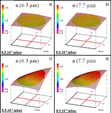
f). Figure 4 presents the variation of the refractive indices of the Ge28.1Sb6.3Se65.6 and Ge12.5Sb25Se62.5 thin films in
Figure 3. Variation of the refractive index (1.55 µm) of the Ge28.1Sb6.3Se65.6 thin films for (a) a fixed
deposition time of 95 min, (b) a fixed working power of 17 W, (c) a fixed Ar pressure of 8.9.10−3 mbar and the
Ge12.5Sb25Se62.5 thin films for (d) a fixed deposition time 95 min, (e) a fixed working power 15 W, (f) a fixed Ar
pressure 8.9.10−3 mbar.
Figure 4. Variation of the refractive index of the thin films for a fixed Ar pressure (a) Ge28.1Sb6.3Se65.6,
near-IR (λ = 1.55 µm) varies from 2.41 to 2.56 and from 2.83 to 2.93 for the Ge28.1Sb6.3Se65.6 and Ge12.5Sb25Se62.5
thin films, respectively. The Ar pressure has a predominant influence on the refractive index and a large decrease of the response is observed when the Ar pressure increases. The deposition time and the working power have almost no effect on the refractive index (Fig. 3c and f). Indeed, when the Ar pressure is fixed at 8.9.10−3 mbar,
variation of the refractive index considering the uncertainty of ellipsometry (0.01) and experimental variance is weak, almost unnoticeable for the Ge12.5Sb25Se62.5 thin films (n (1.55 µm) = 2.89–2.88) and there is no variation for
the Ge28.1Sb6.3Se65.6 thin films (n (1.55 µm) = 2.53). This behavior is confirmed by the results in mid-IR following
a classical chromatic dispersion. The refractive index in mid-IR (6.3 µm), for a fixed Ar pressure 8.9.10−3 mbar
and for the two compositions (Ge28.1Sb6.3Se65.6 and Ge12.5Sb25Se62.5), has a very weak variation (0.01), as shown
in Fig. 4. Results in near-IR (1.55 µm) and in mid-IR (6.3 µm and 7.7 µm) are correlated; refractive indices have the same behavior whatever the wavelength is. Linearity of the response is observed between the refractive index in near-IR and mid-IR. The variation of the refractive index of as–deposited films is usually mostly driven by a chemical composition change and/or a change in the morphology of the thin film resulting from the Ar pressure change35. For the Ge
28.1Sb6.3Se65.6 thin films, the lowest refractive indices are observed for a deficiency in Ge and
an excess in Se. For the Ge12.5Sb25Se62.5 thin films, when the deficiency in selenium element is lower, the
refrac-tive indices are also lowest. Considering Ge-Sb-Se bulk glasses, the refracrefrac-tive index and density are decreasing when germanium content is increasing for a fixed antimony concentration and an over-stoichiometric selenium concentration. The decrease in the refractive index cannot be explained by a change in the composition. It can be underlined that the Ar pressure is the most predominant factor for both compositions and all over the range of wavelengths considered (in near and mid-IR).
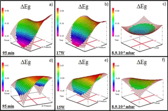
Band-gap energy.
To determine the influence of deposition parameters on the band-gap energy, ΔEg waschosen as ∆ =Eg E (thin film)g −E (target)g . The band-gap energy (±0.01 eV) values of the Ge28.1Sb6.3Se65.6 and
Ge12.5Sb25Se62.5 targets were extracted from VASE data as 2.01 and 1.62 eV. The variations of ΔEg for the
Ge28.1Sb6.3Se65.6 and Ge12.5Sb25Se62.5 thin films based on VASE data are presented in Fig. 5 for a fixed deposition
time (95 min, a and d), a fixed working power 17 W (Ge28.1Sb6.3Se65.6) and 15 W (Ge12.5Sb25Se62.5) (b and e) and for
a fixed Ar pressure 8.9.10−3 mbar (c and f).
Concerning the Ge28.1Sb6.3Se65.6 thin films, ΔEg varies from −0.23 to −0.08 eV (average: −0.14 eV; deviation:
0.01 eV). This means that the band-gap energy of the thin films is systematically lower than that one of the target. The Ar pressure is the preponderant factor while the deposition time and the working power have a small influ-ence on the response. In fact, for a fixed deposition time of 95 min, ΔEg varies from −0.23 eV to −0.08 eV; for a
fixed working power 17 W, ΔEg varies from −0.22 eV to −0.13 eV while for a fixed Ar pressure 8.9.10−3 mbar, the
variation of ΔEg is much weaker, from −0.15 eV to −0.17 eV. An increase of the Ar pressure (from 5.10−3 mbar to
5.10−2 mbar) leads to a decrease of ΔE
g variation (from −0.23 eV to −0.13 eV).
The results for the Ge12.5Sb25Se62.5 thin films are different; a clear influence of each factor (Ar pressure, working
power and deposition time) is observed. ΔEg varies from −0.15 to 0.03 eV (average: −0.05 eV, deviation: 0.01 eV). Figure 5. Variation of ΔEg of the Ge28.1Sb6.3Se65.6 thin films for (a) a fixed deposition time of 95 min, (b) a fixed
working power of 17 W, (c) a fixed Ar pressure of 8.9.10−3 mbar and the Ge
12.5Sb25Se62.5thin films for (d) a fixed
Therefore, the band-gap energy of the Ge12.5Sb25Se62.5 thin films can be lower or slightly higher than the band-gap
energy of the target. A decrease of the response is noted for different factors set combining a high Ar pressure to a high working power (deposition time 95 min, ΔEg = −0.12 eV), a high Ar pressure to a long deposition time
(working power 15 W, ΔEg = −0.12 eV) or a low Ar pressure associated to a low working power (deposition time
95 min, ΔEg = −0.14 eV).
Variation of the band-gap energy is mainly due to the variation of the chemical composition, such as Se defi-ciency and Sb excess, the variation of a glass network structure, the variation of defects affected by deposition parameters38. All these variation will generate a modification of the electronic band structure: a change in the
contribution of Se lonely electron pairs, of bonding electrons involved in homopolar bonds and of Ge-Se, Sb-Se bonds forming the top of the valence band. The influence of deposition parameters on Eg differs according to
the target. Globally, the Ge28.1Sb6.3Se65.6 thin films tend to have smaller Eg than the target which can be mainly
explained by the deficiency of selenium in case of higher ΔEg. Whereas the Ge12.5Sb25Se62.5 thin films tend to have
stable Eg close to the target especially for a low working power even if a Se deficit of 2–3% is observed. The
differ-ent behavior of the two targets is likely related to the Ge/Sb ratio difference influencing the electronic structure of the amorphous network. The systematic negative values of ΔEg of Ge28.1Sb6.3Se65.6 whatever the composition or
the ΔEg ~ 0 eV of Ge12.5Sb25Se62.5 even if a Se deficit of 2–3% have probably origin in the glass network structure
variation and defects formation compare to the bulk glass target. Further study will be performed to better under-stand the band-gap variation according to the deposition parameters.
Deposition rate.
Thin films thicknesses determined from VASE data (±1 nm) were used to determine dep-osition rates. The depdep-osition rates range from 5 to 38 nm.min−1 and from 7 to 33 nm.min−1 for Ge28.1Sb6.3Se65.6
and Ge12.5Sb25Se62.5, respectively (Tables 3 and 4). The results are the same for both compositions: an Ar pressure
and a working power are the two influential factors while deposition time has no effect on the response (Fig. 6). An increase of the deposition rate is observed for a low Ar pressure and a high working power. In the classical sputtering regime, the sputtering yield increases linearly with an incident ion energy and in many cases, the deposition rate goes up with the working power43. The deposition rate is usually decreased by a higher pressure if
the sputtered particles will undergo multiple collisions and thermalization during the transfer to the substrate45.
For a fixed deposition time (95 min), the deposition rates vary from 5 to 38 nm.min−1 and from 7 to 33 nm.min−1
for the Ge28.1Sb6.3Se65.6 (Fig. 6a) and Ge12.5Sb25Se62.5 (Fig. 6d) thin films, respectively. When a working power is
fixed (17 W), the deposition rates vary from 8 to 23 nm.min−1 for the Ge
28.1Sb6.3Se65.6 thin films (Fig. 6b) and
from 12 to 21 nm.min−1 for the Ge
12.5Sb25Se62.5 thin films (Fig. 6e). At Ar pressure of 8.9.10−3 mbar, the
deposi-tion rates vary from 8 to 35 nm.min−1 for the Ge
28.1Sb6.3Se65.6 thin films (Fig. 6c) and from 12 to 33 nm.min−1 for
the Ge12.5Sb25Se62.5 thin films (Fig. 6f). It can be concluded that a working power is the most influential factor;
the variation of this deposition parameter induces a large variation of the deposition rate. For a long deposition
Figure 6. Variation of the deposition rate of the Ge28.1Sb6.3Se65.6 thin films for (a) a fixed deposition time of
95 min, (b) a fixed working power of 17 W, (c) a fixed Ar pressure of 8.9.10−3 mbar and the Ge
12.5Sb25Se62.5 thin
films for (d) a fixed deposition time of 95 min, (e) a fixed working power of 15 W, (f) a fixed Ar pressure of 8.9.10−3 mbar.
experiment, there is no variation of the deposition rate; therefore thicknesses of thick layers (1–5 µm) for an opti-cal structure can be easily controlled.
AFM Surface roughness.
The surface roughness of the Ge28.1Sb6.3Se65.6 thin films varies from 0.37 to6.46 nm (Table 3). Figure 7a presents the variation of the surface roughness for a fixed deposition time of 95 min (0.4 to 4.6 nm); the response decreases when the Ar pressure decreases and the working power has no clear effect. For a fixed working power of 17 W (Fig. 7b), the surface roughness varies from 0.4 to 5.2 nm; as the working power, the deposition time has almost no effect dissimilar to the Ar pressure. Finally, for a fixed Ar pressure of 8.9.10−3 mbar (Fig. 7c), the surface roughness varies from 1.1 to 1.5 nm and the response decreases slightly for
a short deposition time and a low working power. It can be concluded that the Ar pressure has a predominant influence. Especially in the domain of the low Ar pressure, the working power and the deposition time have no effect on the surface roughness. The surface roughness of the Ge12.5Sb25Se62.5 thin films (Table 4) has a similar
comportment to the Ge28.1Sb6.3Se65.6 thin films; it ranges from 0.45 to 6.26 nm. For a fixed deposition time of
95 min (Fig. 7d), the surface roughness varies from 0.45 to 5.2 nm and the response decreases for a low Ar pres-sure and for an intermediate working power. For a fixed working power 15 W (Fig. 7e), the surface roughness varies from 0.45 to 5.7 nm; the response is lower for a low Ar pressure and the deposition time has no effect for a low Ar pressure. In the same way, for a fixed Ar pressure 8.9.10−3 mbar (Fig. 7f), the surface roughness varies
from 0.5 to 2.0 nm and the lower values (0.5 nm) are obtained for an intermediate working power. To conclude, the Ar pressure is the most influential factor and allows obtaining a wide range of the surface roughness. For a low Ar pressure (<1.6.10−2 mbar), the working power and the deposition time have a small influence. However, the
surface roughness slightly decreases for a short deposition time and for an intermediate working power. In order to reduce optical losses in the optical waveguides, the thin films with a low surface roughness are required. The deposition parameter that seems to be the most suitable is a lower Ar pressure (≤1.6.10−2 mbar).
The working power has also a small influence on the surface roughness, especially for a low Ar pressure, an appro-priate working power is intermediate for Ge12.5Sb25Se62.5.
Methods
The glass targets for RF magnetron sputtering of the thin films (GeSe2)100−x(Sb2Se3)x with the nominal
compo-sition of Ge28.1Sb6.3Se65.6 (x = 10) and Ge12.5Sb25Se62.5 (x = 50) were prepared using the conventional method of
melting and quenching from high-purity elements (5 N). Selenium had been previously purified by a static dis-tillation. The elements were weighted in an appropriate amount, inserted in a specific silica glass ampoule under vacuum and then sealed. The elements had been melted in a rocking furnace at 850 °C and then the ampoules with the melt were quenched. The resulting glasses were annealed at a temperature close to their glass transition temperature (Tg): at ~330 and ~205 °C for Ge28.1Sb6.3Se65.6 and Ge12.5Sb25Se62.5, respectively. Chalcogenide glass Figure 7. Variation of the surface roughness of the Ge28.1Sb6.3Se65.6 thin films for (a) a fixed deposition time
of 95 min, (b) a fixed working power of 17 W, (c) a fixed Ar pressure of 8.9.10−3 mbar and the Ge
12.5Sb25Se62.5
thin films for (d) a fixed deposition time of 95 min, (e) a fixed working power of 15 W, (f) a fixed Ar pressure of 8.9.10−3 mbar.
discs with a diameter of 50 mm and a thickness of 3.5 mm were obtained after cutting of the glass rods followed by polishing. The glass discs were used as sputtering targets for a thin films deposition. The chalcogenide thin films were deposited by RF magnetron sputtering on silicon substrates. The deposition was carried out at a work-ing Ar pressure in a range of 5.10−2–5.10−3 mbar. The sputtering was maintained at a low RF working power
(10–25 W) considering the insulator character of the targets and the requirement of amorphous layers fabrication. An off-axis substrates rotation was operated during the deposition process. The silicon substrates were positioned at the target-to-substrate distance of 5 cm.
Thin films characterization.
The chemical composition of the Ge28.1Sb6.3Se65.6 and Ge12.5Sb25Se62.5 thinfilms were measured using a scanning electron microscope with an EDS (JSM 6400-OXFORD Link INCA). Linear refractive indices spectral dependencies of the thin films, thicknesses, consequently deposition rates, as well as optical band-gap values (Eg), were obtained from the analysis of VASE data measured using two
ellipsom-eters56: a rotating analyzer ellipsometer measuring in UV-Vis-NIR (300–2300 nm) and a rotating compensator
ellipsometer working in mid-IR (~1.7–30 µm) (both J. A. Woollam Co., Inc., Lincoln, NE, USA). The VASE meas-urements parameters are as follows: angles of incidence of 65°, 70° and 75°, resolution of UV-Vis-NIR ellipsome-ter of 20, 10 and 5 nm, resolution of the mid-IR ellipsomeellipsome-ter of 2, 8 and 16 cm−1. The used resolution was selected
in accordance with the estimated thickness of the thin films. The Cody-Lorentz model57, 58 was used to analyze
VASE data. This model is appropriate for the description of amorphous chalcogenide optical functions59. The
chalcogenide thin films roughness was studied by an atomic-force microscopy (AFM, Ntegra Prima, NT-MDT). The tapping mode imaging was used on an area of 1 µm × 1 µm.
Conclusions
In summary, Ar pressure, working power and deposition time were selected as potentially the most influential factors for the chalcogenide thin film deposition in the experimental design approach. The results of the experi-mental design analysis confirm the great influence of the Ar pressure. It appears clearly that all responses studied here are influenced by the Ar pressure: the chemical composition, the refractive index in near-IR (1.55 µm) and mid-IR (6.3 µm and 7.7 µm), the band-gap energy, the deposition rate and the surface roughness. Globally, the composition presents some deficit in selenium and an excess of germanium while antimony content is more sta-ble, in good agreement with their sputtering yields. The thin films tend to better reflect the chemical composition of the target for a high Ar pressure. The band-gap energy and the surface roughness are also mainly affected by the Ar pressure while the deposition time and the working power have almost no effects. The deposition rate is strongly changed by the working power (increasing with the power), and to some extend by the high Ar pressure which is reducing it. Moreover, refractive indices are highly influenced by the Ar pressure; a significant decrease is observed for an increase of the pressure related to an important change of the morphology/porosity and the roughness of the films.
Depending on the intended applications and therefore desired thin films characteristics, mappings of the experimental design help to select suitable deposition parameters. To elaborate an optical waveguide composed of buffer and core selenide layers for sensor applications10, 38, 39: a stable composition during deposition not so
far from a target composition, a low surface roughness, a constancy of the refractive index contrast between the two layers and a high deposition rate for the buffer layer are desired. To better respond to these characteristics, it is necessary to work with the most suitable Ar pressure. Working with an intermediate Ar pressure of about 1.10−2 mbar seems to be a good compromise maintaining an adequate stable composition, a low roughness, no
porosity and a suitable refractive index contrast between the two targets. A power of 20 W is preferred for the Ge28.1Sb6.3Se65.6 target, serving as the buffer layer due to a lower refractive index, with the deposition rate of 33 nm/
min allowing deposition of a thick layer. For the Ge12.5Sb25Se62.5 thinner layer, a lower power of about 10 W is
pre-ferred due to necessity to stabilize the refractive index and the composition during the deposition process with a lower deposition rate of about 11 nm/min and a quite low roughness required for a core layer. Furthermore, to complete this study, a structural analysis by Raman spectroscopy and XPS was performed to investigate the influ-ence of the Ar pressure on structural features of the sputtered amorphous films38. However, further investigation
will be performed in order to better understand the behavior of the band-gap of the Ge-Sb-Se sputtered films.
References
1. Rodenas, A. et al. Three-dimensional mid-infrared photonic circuits in chalcogenide glass. Opt. Lett. 37, 392–394 (2012). 2. Sanghera, J. S., Shaw, L. B. & Aggarwal, I. D. Chalcogenide Glass-Fiber-Based Mid-IR Sources and Applications. IEEE J. Sel. Top.
Quantum Electron. 15, 114–119, doi:10.1109/jstqe.2008.2010245 (2009).
3. Eggleton, B. J., Luther-Davies, B. & Richardson, K. Chalcogenide photonics. Nat. Photonics 5, 141–148, doi:10.1038/ nphoton.2011.309 (2011).
4. Anne, M. L. et al. Chalcogenide Glass Optical Waveguides for Infrared Biosensing. Sensors 9, 7398–7411, doi:10.3390/s90907398 (2009).
5. Seddon, A. B. Mid-infrared (IR)–A hot topic: The potential for using mid-IR light for non-invasive early detection of skin cancer in
vivo. Physica Status Solidi B-Basic Solid State Physics 250, 1020–1027, doi:10.1002/pssb.201248524 (2013).
6. Le Corvec, M. et al. Fast and Non-Invasive Medical Diagnostic Using Mid Infrared Sensor The AMNIFIR Project. Irbm 37, 116–123, doi:10.1016/j.irbm.2016.03.003 (2016).
7. Han, Z. et al. On-chip mid-infrared gas detection using chalcogenide glass waveguide. Appl. Phys. Lett. 108, doi:141106 10.1063/1.4945667 (2016).
8. Singh, V. et al. Mid-infrared materials and devices on a Si platform for optical sensing. Science and Technology of Advanced Materials 15, doi:014603 10.1088/1468-6996/15/1/014603 (2014).
9. Ganjoo, A., Jain, H., Yu, C., Irudayaraj, J. & Pantano, C. G. Detection and fingerprinting of pathogens: Mid-IR biosensor using amorphous chalcogenide films. J. Non-Cryst. Solids 354, 2757–2762, doi:10.1016/j.jnoncrysol.2007.09.095 (2008).
10. Aldo, G.-A. et al. Theoretical study of an evanescent optical integrated sensor for multipurpose detection of gases and liquids in the Mid-Infrared. Sensors and Actuators B: Chemical 242, 842–848, doi:10.1016/j.snb.2016.09.174 (2017).
11. Baudet, E. et al. Selenide sputtered films development for MIR environmental sensor. Optical Materials Express 6, 2616–2627, doi:10.1364/ome.6.002616 (2016).
12. Hu, J. et al. Flexible integrated photonics: where materials, mechanics and optics meet Invited. Optical Materials Express 3, 1313–1331, doi:10.1364/ome.3.001313 (2013).
13. Merklein, M. et al. Enhancing and inhibiting stimulated Brillouin scattering in photonic integrated circuits. Nature Communications 6, doi:10.1038/ncomms7396 (2015).
14. Charrier, J. et al. Evanescent wave optical micro-sensor based on chalcogenide glass. Sensors and Actuators B-Chemical 173, 468–476, doi:10.1016/j.snb.2012.07.056 (2012).
15. Huang, C. C. & Hewak, D. W. High-purity germanium-sulphide glass for optoelectronic applications synthesised by chemical vapour deposition. Electron. Lett. 40, 863–865 (2004).
16. Marquez, E. et al. Controlling the optical constants of thermally-evaporated Ge10Sb30S60 chalcogenide glass films by photodoping with silver. J. Non-Cryst. Solids 274, 62–68 (2000).
17. Ivanova, Z. G., Koughia, K., Tonchev, D., Pivin, J. C. & Kasap, S. O. Photoluminescence in Er-implanted amorphous Ge-S-Ga thin films. Journal of Optoelectronics and Advanced Materials 7, 1271–1276 (2005).
18. Vigreux, C. et al. Evidence of a minimum in refractive indexes of amorphous GexTe100-x films: Relevance to the development of infrared waveguides. Physica Status Solidi a-Applications and Materials Science 211, 932–937, doi:10.1002/pssa.201330407 (2014). 19. Youden, K. E. et al. Pulsed-Laser Deposition of Ga-La-S Chalcogenide Glass Thin-Film Optical Wave-Guides. Appl. Phys. Lett. 63,
1601–1603 (1993).
20. Nemec, P. et al. Pulsed laser deposition of pure and praseodymium-doped Ge-Ga-Se amorphous chalcogenide films. Optical
Materials 15, 191–197 (2000).
21. Frumar, M. et al. Thin chalcogenide films prepared by pulsed laser deposition - new amorphous materials applicable in optoelectronics and chemical sensors. J. Non-Cryst. Solids 352, 544–561 (2006).
22. Nazabal, V. et al. Dysprosium doped amorphous chalcogenide films prepared by pulsed laser deposition. Optical Materials 29, 273–278 (2006).
23. Zakery, A., Ruan, Y., Rode, A. V., Samoc, M. & Luther-Davies, B. Low-loss waveguides in ultrafast laser-deposited As2S3 chalcogenide films. Journal of the Optical Society of America B-Optical Physics 20, 1844–1852 (2003).
24. Ramachandran, S. & Bishop, S. G. Excitation of Er3+ emission by host glass absorption in sputtered films of Er-doped
Ge10As40Se25S25 glass. Appl. Phys. Lett. 73, 3196 (1998).
25. Nazabal, V. et al. Sputtering and Pulsed Laser Deposition for Near- and Mid-Infrared Applications: A Comparative Study of Ge25Sb10S65 and Ge25Sb10Se65 Amorphous Thin Films. Int. J. Appl. Ceram. Technol. 8, 990–1000, doi:10.1111/j.1744-7402.2010.02571.x (2011).
26. Frantz, J. A., Shaw, L. B., Sanghera, J. S. & Aggarwal, I. D. Waveguide amplifiers in sputtered films of Er3+- doped gallium lanthanum
sulfide glass. Opt. Express 14, 1797–1803 (2006).
27. Nemec, P. et al. Pulsed laser deposited amorphous chalcogenide and alumino-silicate thin films and their multilayered structures for photonic applications. Thin Solid Films 539, 226–232, doi:10.1016/j.tsf.2013.04.013 (2013).
28. Nazabal, V. et al. Sputtering and Pulsed Laser Deposition for Near- and Mid-Infrared Applications: A Comparative Study of Ge25Sb10S65 and Ge25Sb10Se65 Amorphous Thin Films. Int. J. Appl. Ceram. Technol. 8, 990–1000, doi:10.1111/j.17447402.2010.02571.x
(2011).
29. Nazabal, V. et al. Chalcogenide coatings of Ge15Sb20S65 and Te20As30Se50. Appl. Opt. 47, C114–C123 (2008).
30. Charrier, J. et al. Sulphide GaxGe25-xSb10S65 (x = 0, 5) sputtered films: fabrication and optical characterisation of planar and rib optical waveguides. J. Appl. Phys. 104, 073110 (2008).
31. Seddon, A. B. et al. Mid-infrared integrated optics: versatile hot embossing of mid-infrared glasses for on-chip planar waveguides for molecular sensing. Optical Engineering 53, doi:07182410.1117/1.oe.53.7.071824 (2014).
32. Mittal, V., Wilkinson, J. S. & Murugan, G. S. High-contrast GeTe4 waveguides for mid-infrared biomedical sensing applications.
Proc. SPIE 8988, Integrated Optics: Devices, Materials, and Technologies XVIII, 89881A, doi:10.1117/12.2036972 (2014).
33. Turnbull, D. A., Sanghera, J. S., Nguyen, V. & Aggarwal, I. D. Fabrication of waveguides in sputtered films of GeAsSe glass via photodarkening with above bandgap light. Mater. Lett. 58, 51–54 (2003).
34. Balan, V., Vigreux, C. & Pradel, A. Chalcogenide thin films deposited by radio-frequency sputtering. Journal of Optoelectronics and
Advanced Materials 6, 875–882 (2004).
35. Verger, F. et al. RF sputtered amorphous chalcogenide thin films for surface enhanced infrared absorption spectroscopy. Optical
Materials Express 3, 2112–2131, doi:10.1364/ome.3.002112 (2013).
36. Němec, P. et al. Optical properties of (GeSe2)100−x(Sb2Se3)x glasses in near- and middle-infrared spectral regions. Mater. Res. Bull. 51, 176–179, doi:10.1016/j.materresbull.2013.11.050 (2014).
37. Olivier, M. et al. Structure, nonlinear properties, and photosensitivity of (GeSe2)100−x(Sb2Se3)x glasses. Optical Materials Express 4, 525–540, doi:10.1364/ome.4.000525 (2014).
38. Baudet, E. et al. Structural analysis of RF sputtered Ge-Sb-Se thin films by Raman and X-ray photoelectron spectroscopies. J.
Non-Cryst. Solids 444, 64–72, doi:10.1016/j.jnoncrysol.2016.04.017 (2016).
39. Gutierrez-Arroyo, A. et al. Optical characterization at 7.7 m of an integrated platform based on chalcogenide waveguides for sensing applications in the mid-infrared. Opt. Express 24, 23109–23117, doi:10.1364/oe.24.023109 (2016).
40. Baudet, E. et al. MIR attenuated total reflection sensor for the detection of aromatic hydrocarbons in water. submitted (2017). 41. Doehlert, D. H. Uniform shell designs. The Royal Statistical Society Series C-Applied Statistics 19, 231 (1970).
42. Mathieu, D., Nony, J. & Phan Tan Luu, R. Software NEMRODW (LPRAI-Marseille). (2000).
43. Mattox, D. M. In Handbook of Physical Vapor Deposition (PVD) Processing (Second Edition) 237–286 (William Andrew Publishing, 2010).
44. Rossnagel, S. Handbook of Thin-Film Deposition Processes and Techniques - Principles, Methods, Equipment and Applications (2nd Edition)-chap 8-Sputtering and Sputter Deposition. (2002).
45. Wasa, K. Handbook of Sputtering Technology (Second Edition). (William Andrew Publishing, 2012).
46. Sigmund, P. Theory of Sputtering.I. Sputtering Yield of Amorphous and polycrystalline targets. Physical Review 184, 383, doi:10.1103/PhysRev.184.383 (1969).
47. Seah, M. P. An accurate semi-empirical equation for sputtering yields, II: for neon, argon and xenon ions. Nuclear Instruments &
Methods in Physics Research Section B-Beam Interactions with Materials and Atoms 229, 348–358, doi:10.1016/j.nimb.2004.12.129 (2005).
48. Seah, M. P., Clifford, C. A., Green, F. M. & Gilmore, I. S. An accurate semi-empirical equation for sputtering yields I: for argon ions.
Surface and Interface Analysis 37, 444–458, doi:10.1002/sia.2032 (2005).
49. Matsunami, N. et al. Energy-Dependence of the Ion-Induced Sputtering Yields of Monatomic Solids. Atomic Data and Nuclear Data
Tables 31, 1–80, doi:10.1016/0092-640x(84)90016-0 (1984).
50. Yamamura, Y. & Tawara, H. Energy dependence of ion-induced sputtering yields from monatomic solids at normal incidence.
Atomic Data and Nuclear Data Tables 62, 149–253, doi:10.1006/adnd.1996.0005 (1996).
51. Sharda, S., Sharma, N., Sharma, P. & Sharma, V. Finger prints of chemical bonds in Sb–Se–Ge and Sb–Se–Ge–In glasses: A Far-IR study. J. Non-Cryst. Solids 362, 136–139, doi:10.1016/j.jnoncrysol.2012.10.035 (2013).
52. Rao, K. J. & Mohan, R. Chemical bond approach to determining conductivity band gaps in amorphous chalcogenides and pnictides.
Solid State Commun. 39, 1065–1068, doi:10.1016/0038-1098(81)90209-X (1981).
53. Tichý, L. & Tichá, H. Covalent bond approach to the glass-transition temperature of chalcogenide glasses. J. Non-Cryst. Solids 189, 141–146, doi:10.1016/0022-3093(95)00202-2 (1995).
54. Adam, J.-L. & Zhang, X. H. Chalcogenide Glasses: Preparation, properties and application. Woodhead Publishing series in Electronic
and Optical Materials 44 (2014).
55. Thompson, M. W. Energy Spectrum of Ejected Atoms During High Energy Sputtering of Gold. Philosophical Magazine 18, 377, doi:10.1080/14786436808227358 (1968).
56. Woollam, J. A. et al. In Characterization and Metrology for Ulsi Technology 2000, International Conference Vol. 550 AIP Conference Proceedings 511–518 (Amer Inst Physics, 2001).
57. Jellison, G. E. & Modine, F. A. Parameterization of the optical functions of amorphous materials in the interband region (vol 69, pg 371, 1996). Appl. Phys. Lett. 69, 2137–2137, doi:10.1063/1.118155 (1996).
58. Ferlauto, A. S. et al. Analytical model for the optical functions of amorphous semiconductors from the near-infrared to ultraviolet: Applications in thin film photovoltaics. Journal of Applied Physics 92, 2424–2436, doi:10.1063/1.1497462 (2002).
59. Nemec, P. et al. Photo-stability of pulsed laser deposited GexAsySe100-x-y amorphous thin films. Opt. Express 18, 22944–22957 (2010).
Acknowledgements
This work was financially supported by the Region Bretagne, IFREMER and BRGM through an interCarnot fund, LOUISE ANR project, and Czech Science Foundation (Project No. 16-17921S).
Author Contributions
V.N. planned and managed the project, E.B., PhD student, performed the experiments with the help of V.N. and P.N., E.B., P.N. and V.N. analyzed the data with great help of C.C. (a specialist of XPS and physics of cold plasma) and M.S. who has developed the experimental design approach of this study. L.J. performed SEM and EDS analysis at CMEBA-SCANMAT platform at University of Rennes 1. E.B., M.S., P.N. and V.N. wrote the manuscript with the help of B.B., K.M. and E.R. concerning the final application of these chalcogenide materials devoted to environmental sensors.
Additional Information
Competing Interests: The authors declare that they have no competing interests.
Publisher's note: Springer Nature remains neutral with regard to jurisdictional claims in published maps and
institutional affiliations.
Open Access This article is licensed under a Creative Commons Attribution 4.0 International
License, which permits use, sharing, adaptation, distribution and reproduction in any medium or format, as long as you give appropriate credit to the original author(s) and the source, provide a link to the Cre-ative Commons license, and indicate if changes were made. The images or other third party material in this article are included in the article’s Creative Commons license, unless indicated otherwise in a credit line to the material. If material is not included in the article’s Creative Commons license and your intended use is not per-mitted by statutory regulation or exceeds the perper-mitted use, you will need to obtain permission directly from the copyright holder. To view a copy of this license, visit http://creativecommons.org/licenses/by/4.0/.