Contents lists available atScienceDirect
Applied Surface Science
journal homepage:www.elsevier.com/locate/apsuscFull Length Article
Atomic structure of Sr/Si(0 0 1)(1 × 2) surfaces prepared by Pulsed laser
deposition
Tja
ša Parkelj Potočnik
a,b, Erik Zupani
č
c, Wen-Yi Tong
d, Eric Bousquet
d, Daniel Diaz Fernandez
a,
Gertjan Koster
a,e, Philippe Ghosez
d, Matja
ž Spreitzer
a,⁎aAdvanced Materials Department, Jožef Stefan Institute, Jamova 39, 1000 Ljubljana, Slovenia bJožef Stefan International Postgraduate School, Jamova 39, 1000 Ljubljana, Slovenia
cCondensed Matter Physics Department, Jožef Stefan Institute, Jamova 39, 1000 Ljubljana, Slovenia dTheoretical Materials Physics, Q-MAT, CESAM, University of Liège, B-4000-Liège, Belgium
eFaculty of Science and Technology and MESA+ Institute for Nanotechnology, University of Twente, P.O. Box 217, 7500 AE Enschede, the Netherlands
A R T I C L E I N F O
Keywords: Silicon Strontium
Pulsed laser deposition Scanning tunneling microscopy DFT
Surface defects
A B S T R A C T
A buffer layer formed by depositing a ½ monolayer of Sr on Si(0 0 1) is known to passivate the Si surface, while its surface structure constitutes a suitable template for the integration of various functional oxides with the existing Si platform. We used Pulsed Laser Deposition (PLD) to prepare a Sr/Si(0 0 1)(1 × 2) surface and ana-lysed it using in-situ Reflection High-Energy Diffraction (RHEED) in combination with low-temperature Scanning Tunneling Microscopy (STM). The STM images reveal an atomically ordered surface with terraces composed of one-dimensional (1D) chains running along perpendicular directions on neighbouring terraces. The 1D chains are separated by 0.78 nm and exhibit a low-amplitude corrugation with a period of 0.39 nm. The measured values agree well with the size of the (1 × 2) unit cell observed for similar MBE-grown surfaces, while the density of the surface defects is somewhat higher in the presented case. According to simulated STM images based on DFT calculations, two types of surface defects were identified and explored: arrays of Sr vacancies and Sr adatoms. These results show that PLD can offer precise control for the preparation of high-quality Sr-buffered Si(0 0 1) surfaces.
1. Introduction
The monolithic integration of epitaxial complex oxides with Si is a long-standing objective, since it would allow to incorporate the rich functionalities of complex oxides, such as ferroelectricity, piezo-electricity, magnetism, multiferrocity and high-temperature super-conductivity, with the well-established Si platform, leading to the de-velopment of novel electronic devices with both sensing and logic capabilities[1,2].
The most common template used for the growth of functional complex oxides on Si is based on an epitaxial thinfilm of SrTiO3(STO)
deposited on a Si(0 0 1) surface, forming a STO/Si pseudo-substrate[3]. A crucial step in the preparation of the STO/Si template is the passi-vation of the reactive Si surface. When the native SiO2layer is removed
by annealing in ultra-high vacuum (UHV), each surface Si atom is left with two dangling bonds. One dangling bond per surface atom is sa-turated by pairing with that of an adjacent atom, forming dimers that arrange in rows, and resulting in a double domain (2 × 1)+(1 × 2)
surface reconstruction in the case of vicinal substrates with monoa-tomic steps. It has been shown that the remaining dangling bonds of the Si surface can be successfully passivated by a deposition of 1/2 ML of elemental Sr: the resulting surface displays a SrSi2stoichiometry and
exhibits a (1 × 2)+(2 × 1) reconstruction where the Sr atoms sit be-tween the Si dimer rows, preventing the formation of an amorphous SiO2layer[2].
Apart from Sr other divalent metals like Ba and Eu can be used to form a (1 × 2)+(2 × 1) surface reconstruction on Si(0 0 1)[4,5]. In addition, it was recently shown that in comparison to the Eu/Si(0 0 1) (1 × 2), which is isomorphic to the Sr/Si(0 0 1)(1 × 2) structure, the Eu/Si(0 0 1)(1 × 5) surface structure is a better choice when growing EuO on Si since it enables a formation of a sharp interface[6].
The submonolayer Sr films have been extensively studied both theoretically[7–9]and experimentally by several techniques[10–16]. Recently, an atomic model of the ½ ML Sr on Si(0 0 1)(2 × 1) was proposed based on a combined DFT-STM study [17]. Currently, the main technique used for the preparation of the Sr/Si(0 0 1) surface is
https://doi.org/10.1016/j.apsusc.2018.12.027
Received 10 August 2018; Received in revised form 30 November 2018; Accepted 3 December 2018
⁎Corresponding author.
E-mail address:[email protected](M. Spreitzer).
Available online 04 December 2018
0169-4332/ © 2018 Elsevier B.V. All rights reserved.
Molecular Beam Epitaxy (MBE). However, for the integration of oxides with silicon the low deposition rate, application of only elemental sources andflux monitoring issues make MBE a less ideal tool from the industrial point of view. An alternative technique that provides a tuneable deposition rate and has proven to be very successful in the growth of high-quality complex oxides is pulsed laser deposition (PLD) [18]. PLD is particularly useful when growing materials containing volatile species, for example PZT, which is the key enabler for piezo-MEMS technology[19]. Furthermore, the recent advances in large-area PLD [20], have risen an interest to establish an all-PLD growth of complex oxides on Si.
The process for the preparation of the Sr/Si(0 0 1)(1 × 2) surface by PLD has previously been developed in our group, with its structural properties characterised by in-situ Reflection High-Energy Electron Diffraction (RHEED)[21], and is already in use for the growth of STO on Si(0 0 1) by PLD [22,23]. But while RHEED provides integral in-formation about the surface morphology, it lacks local inin-formation. Given that for PLD the energies of the particles can easily reach up to 100 eV while in MBE the particles impinging the substrate surface have a much lower energy of only a few eV, the density and variety of defects present on surfaces grown by PLD is expected to differ from those on surfaces grown by MBE. Secondly, the base pressure of a typical PLD system is at least an order of a magnitude higher than in MBE systems. Given the high reactivity of the pure Si(0 0 1) surface, the species from the residual atmosphere might influence the quality of the Sr-buffered surface during its preparation. Therefore, an atomic-level analysis of PLD-grown Sr/Si(0 0 1)(1 × 2) surfaces is crucial.
In this work Scanning Tunnelling Microscopy (STM) was used to study the surface morphology, atomic structure and types of defects for a Sr/Si(0 0 1)(1 × 2) surface prepared using PLD, revealing an atom-ically ordered surface structure and surface defects that are unique to the PLD deposition conditions. The interpretation of the origin of the surface defects is supported by STM image simulations based on DFT calculations. The presented results allow us to extract vital information for the development of an all-PLD growth procedure for STO/Sr/Si pseudo-substrates and provides a new insight into Sr-induced Si(0 0 1) surface reconstructions.
2. Material and methods
The samples were prepared in a custom-made PLD chamber (Twente Solid State Technology) equipped with two lasers: a Kr-F ex-cimer laser (λ: 248 nm, 20 ns pulses, Coherent), used for the pulsed ablation, and an IR laser (λ: 800–820 nm, continuous wave, Coherent), used for the substrate heating. The temperature was measured with a pyrometer (85% emissivity, IMPAC). The surface reconstructions were monitored with an in-situ RHEED system (STAIB instruments) using an accelerating voltage of 30 kV. The RHEED diffraction patterns were monitored with a CCD camera and the recorded images were analysed with the KSA 400 commercial software (k-Space Associates). Before every experiment the PLD chamber was baked, which resulted in a base pressure of 2 × 10⁻⁹mbar, with H2, He, H2O, O2and CO2being the
main components of the residual gas. Commercial p-type Si(0 0 1) substrates (B-doped, +/-1°, 1–30 Ωcm, 5 mm × 5 mm, Si-Mat) were cleaned with acetone and ethanol, and then clamped with Ta clips on a hollow Mo holder that allowed direct heating of the substrate from the back side. Before deposition the substrates were degassed at 900 K for 12 h. The native SiO2was removed by annealing at 1470 K for 1 min. A
metallic Sr target (purity 99.9%, Mateck) was used for the Sr deposi-tion. The target was stored in a dry-box with a N2atmosphere, freshly
ground before every experiment and inserted into the PLD chamber without exposure to air. The target was ablated using a 0.14-mm2laser
spot size and afluence of 1 J/cm2at a 55-mm target-to-substrate dis-tance and a 0.25-Hz repetition rate. The low repetition rate was chosen to allow a clear observation of the RHEED pattern transformations during the Sr deposition. A 1/2 ML of Sr was deposited onto the Si
(0 0 1)(2 × 1) surface at 970 K. The amount of deposited Sr needed to complete the 1/2 ML coverage was determined by the appearance of the (2 × 3) surface reconstruction corresponding to the 1/6 ML Sr coverage[9,24].
The samples were transferred from the PLD system to an Ultra-High Vacuum (UHV) system (5 × 10⁻¹¹mbar) equipped with Low-Energy Electron Diffraction (LEED) optics (SPECTRALEED, Scienta Omicron) and a Joule-Thomson STM (SPECS). The transfer was carried out without breaking the vacuum using a custom-built UHV suitcase, equipped with an ion pump, which maintained the pressure below 1 × 10⁻¹⁰mbar. The suitcase was attached to the load-lock of the LEED-STM system, which was baked for 12 h to decrease the base pressure below 5 × 10⁻¹⁰mbar before the samples were inserted. With a total transfer time of 20 h, the total exposure of the sample surfaces was 14 Langmuir (L). After the transfer the stability of a sample surface was inspected using LEED. Before the STM analysis the samples were cooled to 60 K to reduce the thermal drifts and at the same time to ensure sufficient conductivity of the examined surfaces. The STM measurements were performed with an electrochemically etched W tip in the constant-current mode. Prior to the STM imaging the tip was conditioned on a Cu(1 1 1) surface using a controlled tip-sample inter-action. The STM data were processed with the WSxM package[25].
The calculations were performed within the density-functional theory (DFT)[26,27] using the accurate full-potential projector aug-mented wave (PAW) method[28], as implemented in the Vienna ab-initio Simulation Package, VASP (v5.3.3)[29]. The exchange-correla-tion potential was treated in the PBEsol[30]form of the generalized gradient approximation with a kinetic energy cut-off of 600 eV. A 8 × 8 × 1 and a 12 × 12 × 1 Monkhorst-Pack k-point mesh centred at Γ were adopted in the geometry optimization and self-consistent cal-culations, respectively. The electronic configurations were taken into account with valence electrons and pseudopotential versions as: Si (3s23p2, v-05Jan2001), Sr(4s24p65s2, v-07Sep2000), H(1 s1,
v-15Jun2001), C(2s22p2, v-08Apr2002), and O(2s22p4, v-08Apr2002). The convergence criterion for the electronic energy was 10−6eV and the structures were relaxed until the Hellmann–Feynman forces on each atom were < 10 meVnm−1. The Sr/Si(0 0 1) surfaces were modelled using a slab geometry. The simulation substrates consisted offive si-licon layers, as was the case with others[7,31,32]. A large 4 × 4 su-percell with 16Si atoms per atomic layer was adopted to make the re-levant calculations of the interface. The dangling bonds of the Si atoms at the slab bottom were saturated with hydrogen atoms[4,27,28]. To eliminate the spurious slab-slab interactions, a vacuum region of at least 1.5 nm was included between the repeated slabs. The constant-current STM images were simulated within the program HIVE [33] based on the Tersoff-Hamann approximation[34,35].
3. Results and discussion
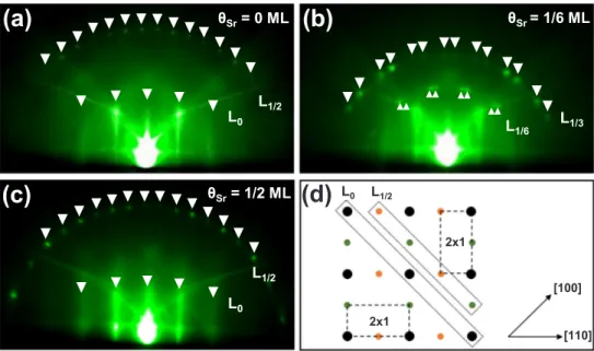
3.1. Controlling the Sr coverage by monitoring Si surface reconstructions In-situ RHEED patterns taken at different growth stages are shown in Fig. 1(a)–(c). The pattern shown inFig. 1(a) was taken after the re-moval of the native SiO2 and consists of well pronouncedfirst-order
streaks in the zeroth Laue zone and spots in the ½ Laue zone corre-sponding to a (2 × 1)+(1 × 2) surface reconstruction. A schematic of the main features of the (2 × 1)+(1 × 2) RHEED patterns is shown in Fig. 1(d). Once the Sr deposition was initiated the (2 × 1)+(1 × 2) reconstruction began to fade and a (2 × 3)+(3 × 2) pattern started to appear. Fig. 1(b) shows a RHEED pattern taken at the peak of the (2 × 3)+(3 × 2) reconstruction that occurs at 1/6 ML coverage, where spots corresponding to the 1/6 and 1/3 Laue arcs can be seen[9]. After further Sr deposition the (2 × 3)+(3 × 2) RHEED pattern gradually transformed into a (1 × 2)+(2 × 1) pattern and reached its maximum intensity at ¼ ML coverage, which persisted until the deposition was terminated at ½ ML of Sr coverage.Fig. 1(c) shows a RHEED pattern
taken after the sample was cooled to room temperature. The narrow first-order streaks and the sharp spots of the (1 × 2)+(2 × 1) re-construction indicate a smooth Sr/Si(0 0 1) surface with a well-defined crystal structure.
3.2. Surface morphology
After the RHEED analysis the samples were transferred to the LEED-STM system without breaking vacuum. The LEED patterns exhibited a clear (1 × 2)+(2 × 1) reconstruction, indicating that the surface re-construction remained unchanged after the transfer as seen in the inset of Fig. 2(a). A large-scale STM image of the Sr/Si(0 0 1) surface in Fig. 2(a) shows a surface composed of terraces separated by single atomic steps (0.14 nm high). Noμm-sized particulates specific to some PLD-grown surfaces were observed. All the terrace edges are jagged, with no significant difference in the degree of roughness between the terrace edges of different domains, as displayed inFig. 2(b).
In comparison the terraces of a clean 2 × 1 reconstructed Si(0 0 1) surface with monoatomic steps exhibit alternating smooth and jagged edges. The smooth-edged terraces are composed of dimer chains run-ning parallel to the terrace edges (A-terraces), while the rough-edged terraces have dimmer rows running perpendicular to the edges (B-ter-races) [36]. When the Sr is deposited at elevated temperatures the morphology of the terrace edges of the Si(0 0 1) surface undergoes a
drastic change as a result of the surface diffusion of Si atoms[15,37]. While the Si dimers remain localized during the Sr deposition at room temperature, the Si atoms from the top-most layer become mobile if the Sr deposition is carried out at temperatures between 700 K and 1000 K [9,15]. The surface therefore undergoes several reconstructions, during which the top layer of Si atoms is re-located. At 1/6 ML Sr coverage, 2/ 3 of the Si dimers are transferred to and incorporated at the terrace edges, forming the 2 × 3 surface reconstruction. As the Sr coverage is further increased, the remaining 1/3 of the Si dimers also move towards the terrace edges, and a (1 × 2) pattern is subsequently formed on the newly exposed Si layer, which exhibits dimer chains rotated by 90° with respect to the original chains and rough terrace edges.
3.3. Atomic structure of the Sr/Si(0 0 1)(1 × 2) surface
High-resolution STM images of the Sr/Si(0 0 1) surface with ½ ML Sr coverage exhibit a well-ordered surface constructed of two different domains, each composed of one-dimensional (1D) chains, running along the [0 1 1] and [0–11] directions on neighbouring terraces, as seen inFig. 3(a). The high-resolution STM image inFig. 3(b) shows a low-amplitude corrugation along the chains with a period of 0.39 nm, while the chains themselves are separated by 0.78 nm. The measured distances agree well with the dimensions of the Si(0 0 1)(2 × 1) surface unit cell (0.384 nm)[36].
(a)
(b)
(c)
L
1/3L
1/6L
1/2L
1/2L
0L
0 (d)(d)
L0 L1/2 [100] [110]θ
Sr= 0 ML
θ
Sr= 1/6 ML
θ
Sr= 1/2 ML
2x1 2x1Fig. 1. RHEED patterns of the Si(0 0 1) sur-face reconstructions for different Sr coverage (θSr): (a) (2 × 1)+(1 × 2) reconstruction of
the deoxidised Si(0 0 1). (b) (2 × 3)+(3 × 2) reconstruction atθSr= 1/6 ML. (c) (1 × 2)
+(2 × 1) reconstruction atθSr= 1/2 ML. All
the RHEED patterns were recoded along the [1 0 0] high-symmetry direction. The Laue zones seen in the RHEED patterns are marked with Lx. (d) The schematic shows the
re-ciprocal lattice of the (2 × 1)+(1 × 2) double domain structure. The larger black and smaller green dots represent the signal from the (2 × 1), while the black and orange dots represent the signal from the (1 × 2) domain.
120 nm
40 nm
(a)
(b)
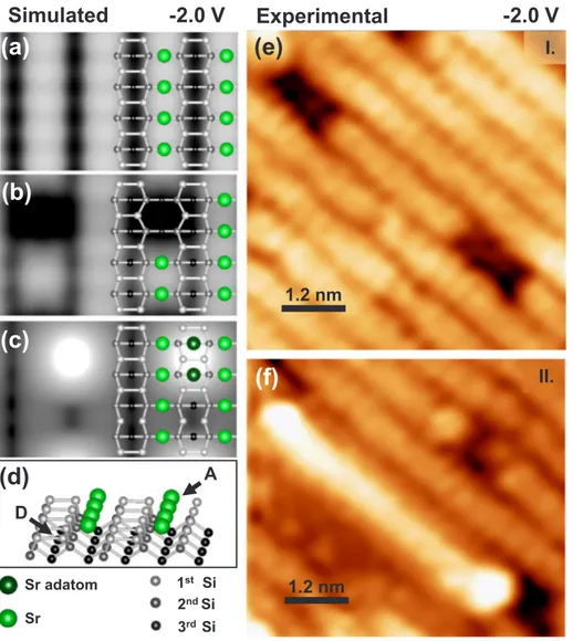
Fig. 2. (a) Large-scale STM image recordedafter the deoxidation of the Si(0 0 1) surface and the deposition of ½ ML of Sr. The re-sulting Sr/Si(0 0 1)(1 × 2) surface exhibits rough-edged terraces, separated by monoa-tomic steps. A LEED pattern of the (1 × 2) +(2 × 1) surface reconstructure recorded at E = 115 eV is shown in the inset. (b) STM image exhibiting the two-domain structure. The STM images were taken at T = 60 K, U = 2 V and I = 50 pA.In order to identify the features in the STM images we performed a DFT study based on a model presented inFig. 4(d). According to our DFT calculations the Sr atoms energetically prefer to sit in the valley-bridge sites between the Si dimer rows (A-site in Fig. 4(d)). By
comparing the calculated filled-state STM images (Fig. 4(a)) to the experimental ones (Fig. 4(e) and (f)), we identified the 1D chains as rows of Sr atoms. Thefilled-state STM images are characterized by single large protrusions, which are related to the Si dangling bonds
II.
I.
A
B
C
(a)
9 nm
(b)
1.2 nm
[110]
[1-10]
Fig. 3. (a) Filled-state STM image of a Sr/Si(0 0 1)(1 × 2) surface composed of 1D chains running in the [0–11] and [0 1 1] directions on neighbouring terraces. Different types of surface defects are marked. (b) A high-resolution filled-state STM image exhibiting corrugation along the 1D chains. For more details, see the text. The STM images were taken at T = 60 K, U = -2V and I = 120 pA.
Sr
1
stSi
2
ndSi
3
rdSi
Sr adatom
Simulated
-2.0 V
Experimental
-2.0 V
1.2 nm
1.2 nm
I.
II.
(a)
(b)
(c)
(e)
(f)
D
A
(d)
Fig. 4. Simulated STM images of the 1 × 2 Sr/Si(0 0 1): (a) the ideal structure, (b) with two Sr vacancies, and (c) with two Sr adatoms. (d) Schematics of the model with marked site A and D. (e) and (f) Magnification of the area I and II ofFig. 3(b) exhibiting an array of Sr vacancies and Sr adatoms, respectively.
participating in the bonding with Sr atoms. This is in agreement with the atomic model proposed by Kuzmin et al.[17].
3.4. Surface defects
Apart from the periodic structures, we observed three types of surface defects, as marked inFig. 3(a). Type-A defects appear as de-pressions along the 1D chains with the measured length and depth ranging typically from 0.5 to 4.5 nm, and from 0.14 to 0.17 nm, re-spectively. Type-B defects appear as arrays of protrusions in-between the 1D chains, while the irregularly shaped and rather large protrusions randomly distributed across the surface are marked as type-C defects. The distribution of these different types of defects is homogeneous across the terraces. Furthermore, we did not observe any variation in the concentration of the defects close to the step edges. The type-A and type-B defects remained stable during STM imaging, even at relatively high bias (up to -3 V) and tunneling currents up to 120 pA, while the type-C defects were often displaced by the STM tip during imaging, even under more moderate tunneling conditions. Thus, we conclude that the type-A and type-B defects were probably formed during the Sr deposition, while the type-C defects represent impurities, adsorbed after the Sr deposition and during the sample transfer from the PLD to the STM system. In order to identify the A and B defects, we performed further DFT calculations.
3.4.1. A-defects: Sr vacancies
To study the origin of the A-defects we simulated afilled-state STM image based on the model of an ideal Sr/Si(0 0 1)(1 × 2) surface with two Sr atoms missing in a single chain of Sr atoms. If Sr vacancies are present, the unfilled Si bonds cause the appearance of depressions in the simulated STM images, which are depicted inFig. 4(b). These calcu-lated results are perfectly consistent with the experimental images shown in Fig. 4(e). Thus, we identified the type-A defects as Sr va-cancies.
As observed inFig. 4(f), the Sr vacancies tend to arrange themselves in arrays along the 1D chains. We calculated the formation energies for a single Sr vacancy (EA= 0.585 eV) and a pair of Sr vacancies in a
single chain (E2A= 0.438 eV). The case with two Sr vacancies possesses
a lower formation energy. This means that it is energetically favourable for the vacancies to pair, decreasing their surface mobility, and forming a nucleation site where other vacancies can agglomerate, forming ar-rays as a result.
This arrangement of vacancies across the Sr/Si(0 0 1)(1 × 2) surface of PLD-grown samples is different to that found in comparable MBE-grown samples. In the latter case, the neighbouring vacancies in the adjacent chains are frequently connected to each other and shifted by a unit cell with respect to each other along the chains. A sequence of such vacancy pairs can even agglomerate in a short chain along the [0 2 1] directions[14,31]. In the case of the MBE-grown samples, the observed Sr vacancies are a consequence of the coverage being below the sa-turation coverage at ½ ML, and for this reason a part of the adsorption sites for Sr atoms can remain unoccupied. In the case of PLD-grown samples the vacancies can be formed in two ways: either they represent unoccupied sites or they were created by removing a primarily ad-sorbed Sr atom during a collision with the impinging Sr species. While the MBE deposition occurs near thermodynamic equilibrium with ki-netic energies of the order of 0.1 eV, the Sr ions in the plasma plume during the PLD deposition can gain up to 100 eV when the deposition is carried out in vacuum, as in our case. Such kinetic energies of the ar-riving species are sufficiently high to form Sr vacancies.
3.4.2. B-defects: Sr adatoms
Based on the comparison between the calculated and experimental images, the B-defects were identified as Sr adatoms adsorbed on top of Si dimers (site D inFig. 4(d)). Similar to Ashman et al.[7], our DFT calculations showed that for cases with Sr adatoms, the global
minimum in energy appears when the Sr sits in the trench between the dimer rows and the centre of 4 surrounding dimers (site A inFig. 4(d)). Site D, located on top of a dimer row in between two dimers, is the second energetically most favoured adsorption site with an energy difference of 0.41 eV. The simulated STM images inFig. 4(c) confirmed that the strong protrusions in the experiments (Fig. 4(f)) correspond to the local density of states of Sr adatoms. We calculated the energy needed to form a single Sr adatom. The resulting energy EB= 1.408 eV
is much higher than the vacancy-formation energy. Furthermore, using the Electron Localization Function (ELF) analysis we explored the nature of the bond, which is mostly ionic (Supp. Fig. 1).
Aside from Sr we also considered alternative adatoms and molecules adsorbed on the D-site of the Sr/Si(0 0 1)(1 × 2) surface that might originate from the residual atmosphere, such as atomic O, atomic C and the CO molecule, or ones that could migrate to the top of the Sr/Si (0 0 1) surface during the surface reconstruction where Si atoms are the most likely candidates. Ourfirst-principles calculations indicated that compared to the Sr case, the distances between the Si surface and these adatoms are relatively small, causing completely different STM features (Supp. Fig. 2). Such theoretical results provide the support to identify the B-defects as Sr adatoms on the D-sites of the Sr/Si(0 0 1) surface.
Surface defects like Sr adatoms have not been observed in MBE-grown surfaces. The energy needed to form a Sr adatom (EB= 1.408 eV) is substantially higher than that for a Sr vacancy
(EA= 0.585 eV). However, such energy can be provided by the
high-energy particles from the plasma plume. Apart from the high mean kinetic energy, the plume vapour can reach a high degree of super-saturation, causing a rapid nucleation of very small clusters, relative to the steady-state deposition at the same average rate[38]. On this basis we propose two possible mechanisms for the formation of Sr adatoms: the displacement of Sr atoms from site A to site D due to high-energy particles impinging on the surface and nucleation caused by the local saturation of Sr atoms.
The overall density of the surface defects in the presented PLD-grown surfaces is higher than in the cases of MBE-PLD-grown surfaces. Primarily, the density of the defects is increased because of the nature of the PLD deposition, while some defects can be related to the higher base pressure in the PLD chamber during the sample preparation. While the Si(0 0 1) surface normally requires a base pressure lower than 5 × 10⁻¹⁰mbar to remain clean for longer periods of time[39], we observed that the surface can be successfully passivated even at a base pressure of 2 × 10⁻⁹mbar if the Sr deposition is carried out in a short time (less than 5 min) after the removal of the native oxide. Overall, we conclude that the Si(0 0 1) surfaces prepared using the presented pro-cedure can be successfully passivated.
4. Conclusions
This study represents thefirst local structural analysis of a PLD-prepared Sr-buffered Si surface. We have shown that PLD can be ap-plied to grow the high-quality Sr-buffered Si surfaces needed for the controlled epitaxial growth of STO and other complex oxides on Si substrates which can lead to an all-PLD integration of complex oxides with silicon.
The preparation of the Sr/Si(0 0 1)(1 × 2) surfaces, performed at elevated temperature using PLD with the Sr coverage increasing from 0 to 1/2 ML, revealed clear transitions from Si(0 0 1)(2 × 1) to Sr/Si (0 0 1)(2 × 3) andfinally to Sr/Si(0 0 1)(1 × 2) in the RHEED images. The morphology and the surface structure, studied with low-tempera-ture STM at an atomic resolution, showed that the ordered part of the surface closely resembles the one in the case of MBE deposition. However, in the case of PLD deposition, the density of the defects was higher and their appearance was different to those found during the MBE deposition. Based on DFT modelling the surface defects were identified as arrays of Sr vacancies and Sr adatoms along with some impurities originating from the residual atmosphere. The presented
results show that the main difference in the types of defects originates from the higher energy of the particles involved in PLD at low pressures compared to that in the MBE growth.
Acknowledgments
This work was supported by the Slovenian Research Agency [grants number PR-06807, J2-6759 and J2-9237] and the international pro-jects: ENPIEZO [M-ERA.NET 3330-14-500197] and SIOX [M-ERA.NET 3330-17-500100]. We acknowledge access to Céci computing facilities funded by F.R.S.-FNRS Belgium [Grant No 2.5020.1] and Tier-1 su-percomputer of the Fédération Wallonie-Bruxelles funded by the Walloon Region [Grant No 1117545]. EB acknowledges F.R.S-FNRS Belgium for support. The authors would like to express their gratitude to Marion van Midden (Condensed Matter Physics Department, Jožef Stefan Institute, Ljubljana, Slovenia) for invaluable help and assistance with the STM measurements and Dejan Klement, Urška Gabor and Zoran Jovanovič (Advanced Materials Department, Jožef Stefan Institute, Ljubljana, Slovenia) for fruitful discussions.
Appendix A. Supplementary material
Supplementary data to this article can be found online athttps:// doi.org/10.1016/j.apsusc.2018.12.027.
References
[1] A.A. Demkov, A.B. Posadas, Integration of Functional Oxides with Semiconductors, (2014).
[2] J.W. Reiner, A.M. Kolpak, Y. Segal, K.F. Garrity, S. Ismail-Beigi, C.H. Ahn, F.J. Walker, Adv. Mater. 22 (2010) 2919–2938.
[3] R.A. McKee, F.J. Walker, M.F. Chisholm, Phys. Rev. Lett. 81 (1998) 3014–3017. [4] K. Ojima, M. Yoshimura, K. Ueda, Phys. Rev. B 65 (2002) 075408.
[5] D.V. Averyanov, C.G. Karateeva, I.A. Karateev, A.M. Tokmachev, M.V. Kuzmin, P. Laukkanen, A.L. Vasiliev, V.G. Storchak, Mater. Des. 116 (2017) 616–621. [6] D.V. Averyanov, C.G. Karateeva, I.A. Karateev, A.M. Tokmachev, A.L. Vasiliev,
S.I. Zolotarev, I.A. Likhachev, V.G. Storchak, Sci. Rep. 6 (2016) 22841. [7] C.R. Ashman, C.J. Först, K. Schwarz, P.E. Blöchl, Phys. Rev. B 69 (2004) 075309. [8] A.A. Demkov, X. Zhang, J. Appl. Phys. 103 (2008) 103710.
[9] K. Garrity, S. Ismail-Beigi, Phys. Rev. B - Condens. Matter Mater. Phys. 80 (2009) 1–14.
[10] W.C. Fan, N.J. Wu, A. Ignatiev, Phys. Rev. B 42 (1990) 1254–1257. [11] Y. Liang, S. Gan, M. Engelhard, Appl. Phys. Lett. 79 (2001) 3591–3593.
[12] A. Herrera-Gómez, F.S. Aguirre-Tostado, Y. Sun, P. Pianetta, Z. Yu, D. Marshall, R. Droopad, W.E. Spicer, J. Appl. Phys. 90 (2001) 6070–6072.
[13] X. Hu, Z. Yu, J.A. Curless, R. Droopad, K. Eisenbeiser, Appl. Surf. Sci. 181 (2001) 103–110.
[14] D.M. Goodner, D.L. Marasco, A.A. Escuadro, L. Cao, M.J. Bedzyk, Phys. Rev. B 71 (2005) 1–6.
[15] J.W. Reiner, K.F. Garrity, F.J. Walker, S. Ismail-Beigi, C.H. Ahn, Phys. Rev. Lett. 101 (2008) 3–6.
[16] M. Choi, A.B. Posadas, H. Seo, R.C. Hatch, A.A. Demkov, Appl. Phys. Lett. 102 (2013) 4–8.
[17] M. Kuzmin, P. Laukkanen, M.P.J. Punkkinen, J. Mäkelä, M. Yasir, J. Dahl, M. Tuominen, K. Kokko, Surf. Sci. 646 (2016) 140–145.
[18] M. Lorenz, M.S. Ramachandra Rao, T. Venkatesan, E. Fortunato, P. Barquinha, R. Branquinho, D. Salgueiro, R. Martins, E. Carlos, A. Liu, F.K. Shan, M. Grundmann, H. Boschker, J. Mukherjee, M. Priyadarshini, N. DasGupta, D.J. Rogers, F.H. Teherani, E.V. Sandana, P. Bove, K. Rietwyk, A. Zaban, A. Veziridis, A. Weidenkaff, M. Muralidhar, M. Murakami, S. Abel, J. Fompeyrine, J. Zuniga-Perez, R. Ramesh, N.A. Spaldin, S. Ostanin, V. Borisov, I. Mertig, V. Lazenka, G. Srinivasan, W. Prellier, M. Uchida, M. Kawasaki, R. Pentcheva, P. Gegenwart, F. Miletto Granozio, J. Fontcuberta, N. Pryds, J. Phys. D. Appl. Phys. 49 (2016).
[19] M.D. Nguyen, E. Houwman, M. Dekkers, D. Schlom, G. Rijnders, APL Mater. 5 (2017) 074201.
[20] D.H.A. Blank, M. Dekkers, G. Rijnders, J. Phys. D. Appl. Phys. 47 (2014) 034006. [21] D. Klement, M. Spreitzer, D. Suvorov, Appl. Phys. Lett. 106 (2015) 071602. [22] D. Diaz-Fernandez, M. Spreitzer, T. Parkelj, J. Kovač, D. Suvorov, RSC Adv. 7
(2017) 24709–24717.
[23] D. Diaz-Fernandez, M. Spreitzer, T. Parkelj, D. Suvorov, Appl. Surf. Sci. 455 (2018) 227–235.
[24] M. Kuzmin, M.P.J. Punkkinen, P. Laukkanen, J.J.K. Lång, J. Dahl, L. Vitos, K. Kokko, J. Phys. Chem. C 118 (2014) 1894–1902.
[25] I. Horcas, R. Fernández, J.M. Gómez-Rodríguez, J. Colchero, J. Gómez-Herrero, A.M. Baro, Rev. Sci. Instrum. 78 (2007) 013705.
[26] P. Hohenberg, W. Kohn, Phys. Rev. 136 (1964) B864–B871. [27] W. Kohn, L.J. Sham, Phys. Rev. 140 (1965) A1133–A1138. [28] P.E. Blöchl, Phys. Rev. B 50 (1994) 17953–17979.
[29] G. Kresse, J. Furthmüller, Comput. Mater. Sci. 6 (1996) 15–50. [30] J.P. Perdew, A. Ruzsinszky, G.I. Csonka, O.A. Vydrov, G.E. Scuseria,
L.A. Constantin, X. Zhou, K. Burke, Phys. Rev. Lett. 100 (2008) 136406. [31] J. Wang, J.A. Hallmark, D.S. Marshall, W.J. Ooms, P. Ordejón, J. Junquera,
D. Sánchez-Portal, E. Artacho, J.M. Soler, Phys. Rev. B 60 (1999) 4968–4971. [32] C.J. Först, C.R. Ashman, K. Schwarz, P.E. Blöchl, Nature 427 (2004) 53–56. [33] D.E.P. Vanpoucke, G. Brocks, Phys. Rev. B 77 (2008) 241308.
[34] J. Tersoff, D.R. Hamann, Phys. Rev. Lett. 50 (1983) 1998–2001. [35] J. Tersoff, D.R. Hamann, Phys. Rev. B 31 (1985) 805–813.
[36] J.E. Griffirh, G.P. Kochanski, Crit. Rev. Solid State Mater. Sci. 16 (1990) 255–289. [37] J. He, G. Zhang, J. Guo, Q. Guo, K. Wu, J. Appl. Phys. 109 (2011) 1–4. [38] S. Metev, K. Meteva, Appl. Surf. Sci. 43 (1989) 402–408.
[39] K. Hata, T. Kimura, S. Ozawa, H. Shigekawa, J. Vac. Sci. Technol. A Vacuum, Surfaces, Film. 18 (2000) 1933–1936.